ICGOO在线商城 > 开发板,套件,编程器 > 评估板 - DC/DC 与 AC/DC(离线)SMPS > LM21212-1EVM
 Datasheet下载
- 型号: LM21212-1EVM
- 制造商: Texas Instruments
- 库位|库存: xxxx|xxxx
- 要求:
| 数量阶梯 | 香港交货 | 国内含税 |
| +xxxx | $xxxx | ¥xxxx |
查看当月历史价格
查看今年历史价格
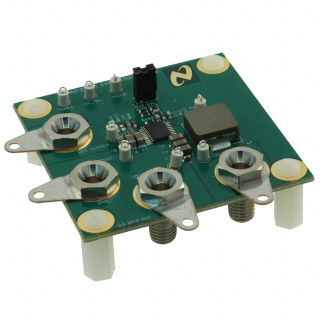
LM21212-1EVM产品简介:
ICGOO电子元器件商城为您提供LM21212-1EVM由Texas Instruments设计生产,在icgoo商城现货销售,并且可以通过原厂、代理商等渠道进行代购。 LM21212-1EVM价格参考。Texas InstrumentsLM21212-1EVM封装/规格:评估板 - DC/DC 与 AC/DC(离线)SMPS, LM21212-1 SIMPLE SWITCHER® DC/DC, Step Down 1, Non-Isolated Outputs Evaluation Board。您可以下载LM21212-1EVM参考资料、Datasheet数据手册功能说明书,资料中有LM21212-1EVM 详细功能的应用电路图电压和使用方法及教程。
Texas Instruments (TI) 的 LM21212-1EVM 是一款用于评估 LM21212 DC/DC 转换器的评估模块。该评估板专为设计和测试高效、高性能的降压(Buck)转换器而设计,适用于多种应用场景。

 应用场景:

1. 工业自动化与控制:
   - 在工业环境中,LM21212-1EVM 可用于评估和开发高效的电源解决方案,特别是在需要高可靠性和低功耗的应用中。例如,工厂自动化设备、PLC(可编程逻辑控制器)、传感器接口等。

2. 通信基础设施:
   - 该评估板适用于电信设备中的电源管理,如基站、路由器、交换机等。它能够提供稳定的电源输出,确保通信系统的稳定运行,同时减少能源浪费。

3. 汽车电子系统:
   - 在汽车行业中,LM21212-1EVM 可用于评估车载电源系统的设计,如车载信息娱乐系统、ADAS(高级驾驶辅助系统)、ECU(电子控制单元)等。它能够在宽输入电压范围内提供稳定的输出电压,适应汽车电气环境的变化。

4. 消费电子产品:
   - 对于消费类电子产品,如笔记本电脑、平板电脑、智能音箱等,LM21212-1EVM 可帮助工程师评估电源效率和热性能,确保产品在长时间使用中的稳定性和安全性。

5. 医疗设备:
   - 在医疗设备中,电源的稳定性和可靠性至关重要。LM21212-1EVM 可用于评估便携式医疗设备、监护仪、超声设备等的电源管理系统,确保设备在各种工作条件下的正常运行。

6. 物联网 (IoT) 设备:
   - 对于低功耗的 IoT 设备,如智能家居传感器、无线网关等,LM21212-1EVM 可以帮助优化电源设计,延长电池寿命,提高系统的整体能效。

 总结:
LM21212-1EVM 主要应用于需要高效、稳定电源管理的领域,包括工业自动化、通信基础设施、汽车电子、消费电子、医疗设备和 IoT 设备等。通过使用该评估板,工程师可以快速验证设计方案,优化电源性能,确保最终产品的可靠性和能效。
| 参数 | 数值 |
| 产品目录 | 编程器,开发系统半导体 |
| 描述 | BOARD EVAL LM21212-1电源管理IC开发工具 LM21212-1EVM EVAL BOARD |
| 产品分类 | |
| 品牌 | Texas Instruments |
| 产品手册 | |
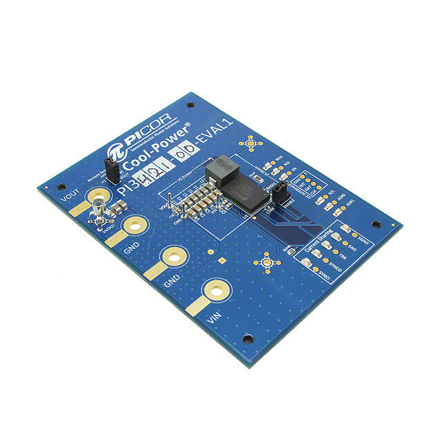
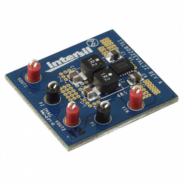
| 产品图片 |
|
| rohs | 否无铅 / 符合限制有害物质指令(RoHS)规范要求 |
| 产品系列 | 电源管理IC开发工具,Texas Instruments LM21212-1EVMSIMPLE SWITCHER® |
| 数据手册 | 点击此处下载产品Datasheethttp://www.ti.com/lit/pdf/snva467 |
| 产品型号 | LM21212-1EVM |
| 主要用途 | DC/DC,步降 |
| 产品 | Evaluation Boards |
| 产品种类 | 电源管理IC开发工具 |
| 使用的IC/零件 | LM21212-1 |
| 制造商产品页 | http://www.ti.com/general/docs/suppproductinfo.tsp?distId=10&orderablePartNumber=LM21212-1EVM |
| 功率-输出 | - |
| 参考设计库 | http://www.digikey.com/rdl/4294959904/4294959903/708 |
| 商标 | Texas Instruments |
| 工具用于评估 | LM21212 |
| 工厂包装数量 | 1 |
| 所含物品 | 板 |
| 板类型 | 完全填充 |
| 标准包装 | 1 |
| 电压-输入 | 2.95 V ~ 5.5 V |
| 电压-输出 | 1.2V |
| 电流-输出 | 12A |
| 稳压器拓扑 | 降压 |
| 类型 | PMIC Solutions |
| 输出和类型 | 1,非隔离 |
| 频率-开关 | 300kHz ~ 1.5MHz |


- 商务部:美国ITC正式对集成电路等产品启动337调查
- 曝三星4nm工艺存在良率问题 高通将骁龙8 Gen1或转产台积电
- 太阳诱电将投资9.5亿元在常州建新厂生产MLCC 预计2023年完工
- 英特尔发布欧洲新工厂建设计划 深化IDM 2.0 战略
- 台积电先进制程称霸业界 有大客户加持明年业绩稳了
- 达到5530亿美元!SIA预计今年全球半导体销售额将创下新高
- 英特尔拟将自动驾驶子公司Mobileye上市 估值或超500亿美元
- 三星加码芯片和SET,合并消费电子和移动部门,撤换高东真等 CEO
- 三星电子宣布重大人事变动 还合并消费电子和移动部门
- 海关总署:前11个月进口集成电路产品价值2.52万亿元 增长14.8%

PDF Datasheet 数据手册内容提取
User's Guide SNVA467B–February2011–RevisedMay2013 AN-2107 LM21212-1 Evaluation Board 1 Introduction ThisevaluationboardprovidesasolutiontoexaminethehighefficiencyLM21212-1buckswitching regulator.TheLM21212-1iscapableofdrivingupto12Aofcontinuousloadcurrentwithexcellentoutput voltageaccuracyduetoits±1%internalreference.Thisdevicealsofeaturesaclocksynchronizationinput thatallowstheswitchingfrequencytobesynchronizedtoanexternalclocksource.The300kHzto1.5 MHzfrequencysynchronizationrangeenablestheusertominimizethepowerstagecomponentsize, whilestillallowingforhighefficiency.TheLM21212-1iscapableofdownconvertingfromaninputvoltage between2.95Vand5.5V.Faultprotectionfeaturesincludecurrentlimit,outputpowergood,andoutput over-voltageprotection.Thedualfunctionsoft-start/trackingpincanbeusedtocontrolthestartup responseoftheLM21212-1,andtheprecisionenablepincanbeusedtoeasilysequencetheLM21212-1 inapplicationswithsequencingrequirements. TheLM21212-1evaluationboardhasbeenoptimizedtoworkfrom2.95Vto5.5V,achievingabalance betweenoverallsolutionsizeandregulatorefficiency.Theevaluationboardmeasuresjustunder2”x2” onafourlayerPCB,andexhibitsajunction-to-ambientthermalimpedance(θ )of24°C/Wwithnoair JA flow.ThepowerstageandcompensationcomponentsoftheLM21212-1evaluationboardhavebeen optimizedforaninputvoltageof5V,butfortestingpurposes,theinputcanbevariedacrosstheentire operatingrange.Theoutputvoltageoftheevaluationboardisnominally1.2V,butthisvoltagecanbe easilychangedtoanyvoltagebetween0.6VandV bymodifyingthefeedbackresistornetwork. IN 2 Evaluation Board Schematic VOUT eTSSOP-20 SWITCH SENSE+ VIN = 2.95V to 5.5V L1 0.56 ØH VIN 11-16 SW VOUT SENSE+ RAC 5,6,7 VIN PVIN AC INJ 49.9(cid:214) GND R1 1(cid:214) CC3 4 C3 C4 C5 C9 GND C1 AVIN RFB1 820 pF 100 ØF 0.1 ØF VOUT SENVSIEN- C810C0 7ØFC6 REN1 1 ØF LM21212-1 19 10 k(cid:214) 1R6C52(cid:214) VOUT = 1.2V, up toS 1E2NASE- open 3 FB ENABLE EN CC1 RC1 REN2 18 2700 pF7.32 k(cid:214) RFB2 open COMP 10 k(cid:214) 2 SS / SS_TRK CSS TRK CC2 0.033 ØF Vin 82 pF 1 RPG SYNC SYNC 10 k(cid:214) 17 PGOOD PGOOD PGND AGND 8,9,10 20 Figure1.EvaluationBoardSchematic Alltrademarksarethepropertyoftheirrespectiveowners. SNVA467B–February2011–RevisedMay2013 AN-2107LM21212-1EvaluationBoard 1 SubmitDocumentationFeedback Copyright©2011–2013,TexasInstrumentsIncorporated
PoweringandLoadingConsiderations www.ti.com 3 Powering and Loading Considerations Readthisentirepagepriortoattemptingtopowertheevaluationboard. 3.1 Quick Setup Procedure 1. Settheinputsourcecurrentlimitto10A.Turnofftheinputsource.Connectthepositiveoutputofthe inputsourcetoV andthenegativeoutputtothecorrespondingGND. IN 2. Connecttheload(with12Acapability)toV forthepositiveconnectionandGNDforthenegative OUT connection. 3. LeavetheENABLEpinopenfornormaloperation. 4. Settheinputsourcevoltageto5V.Theloadvoltageshouldbeinregulationwithanominal1.2V output. 5. SlowlyincreasetheloadwhilemonitoringtheloadvoltageatV .Itshouldremaininregulationwitha OUT nominal1.2Voutputastheloadisincreasedupto12A. 6. Slowlysweeptheinputsourcevoltagefrom2.95Vto5.5V.Theloadvoltageshouldremainin regulationwithanominal1.2Voutput.Ifdesired,theoutputofthedevicecanbedisabledby connectingtheENABLEpintoGND. 7. Connecta2.0Vsquare-wavepositivesignalbetweenSYNCandGNDtovarythefrequencyof operationasdesired. 3.2 Powering Up Itissuggestedthattheloadpowerbekeptlowduringthefirstpowerup.Oncethedeviceispoweredup, immediatelycheckfor1.2Vattheoutput. Aquickefficiencycheckisthebestwaytoconfirmthateverythingisoperatingproperly.Ifsomethingis amissyoucanbereasonablysurethatitwillaffecttheefficiencyadversely.Fewparameterscanbe incorrectinaswitchingpowersupplywithoutcreatinglossesandpotentiallydamagingheat. Somevoltagesuppliescanexhibitseverevoltageovershootduringhighcurrenttransients.Ifasupply overshootsabove6.0V,damagetotheLM21212-1canoccur.Forthesesupplies,alargecapacitoracross theterminalsofthesupply(1000µF)canalleviatethisproblem. 3.3 Over Current Protection Theevaluationboardisconfiguredwithover-currentprotection.Thisfunctioniscompletelycontainedin theLM21212-1.Thepeakcurrentislimitedtoapproximately17A. 2 AN-2107LM21212-1EvaluationBoard SNVA467B–February2011–RevisedMay2013 SubmitDocumentationFeedback Copyright©2011–2013,TexasInstrumentsIncorporated
www.ti.com PoweringandLoadingConsiderations Table1.ConnectionDescriptions TerminalSilkscreen Description VIN Thisterminalistheinputvoltagetothedevice.Theevaluationboardwilloperateovertheinputvoltage rangeof2.95Vto5.5V. GND Theseterminalsarethegroundconnectionstothedevice.Theinputpowergroundshouldbeconnected nexttotheinputV connection,andtheoutputpowergroundnexttotheV connection. IN OUT VOUT Thisterminalconnectstotheoutputvoltageofthepowersupplyandshouldbeconnectedtotheload. ENABLE Thisterminalconnectstotheenablepinofthedevice.Thisterminalcanbeleftfloatingordriven externally.Ifleftfloating,a2µAcurrentsourcewillpullthepinhigh,therebyenablingthedevice.Ifdriven externally,avoltagetypicallylessthan1.2Vwilldisablethedevice. SS/TRK ThisterminalprovidesaccesstotheSS/TRKpinofthedevice.Connectionstothisterminalarenot neededformostapplications.ThefeedbackpinofthedevicewilltrackthevoltageontheSS/TRKpinif itisdrivenwithanexternalvoltagesourcethatisbelowthe0.6Vreference. PGOOD Thisterminalconnectstothepowergoodoutputofthedevice.Thispinispulledupthrougha10kΩ pull-upresistortoV . IN ACINJ ThisterminalblockallowstheusertoinsertanACinjectionsignalacrossa49.9Ωresistorforopen-loop gainbodemeasurements.Ajumpershortsoutthisresistorwhenitisnotneeded. SWITCH Thisterminalallowseasyprobingoftheswitchnode.Donotapplyanyexternalvoltagesourcetothis pin. SYNC ThisterminalconnectstotheSYNCpinofthedevice.TheLM21212-1cansynchronizetheSWITCHpin toaSYNCsignalwithafrequencybetween300kHzand1.5MHz.Ifthispinisleftopen,theswitching frequencywilldefaultto1MHz. VIN_SENSE+, TheseterminalsallowasenseconnectionontheboardforaccurateV andV measurements, IN OUT VIN_SENSE- respectively. VOUT_SENSE+, VOUT_SENSE- SNVA467B–February2011–RevisedMay2013 AN-2107LM21212-1EvaluationBoard 3 SubmitDocumentationFeedback Copyright©2011–2013,TexasInstrumentsIncorporated
PerformanceCharacteristics www.ti.com 4 Performance Characteristics EfficiencyPlots Figure2showstheconversionefficiencyversusoutputcurrentfora5Vinputvoltagefor500kHz,1MHz, and1.5MHzf . SW 96 500kHz 1MHz 94 1.5MHz 92 %) Y ( 90 C EN 88 CI FI 86 F E 84 82 80 0 2 4 6 8 10 12 OUTPUT CURRENT (A) Figure2.ConversionEfficiencyVersusOutputCurrent Turn-onWaveform Asoft-startsequenceoccurswhenapplyingpowertotheLM21212-1evaluationboard.Figure3shows theoutputvoltageduringatypicalstart-upsequence. VOUT (500 mV/Div) VPGOOD (5V/Div) VENABLE (5V/Div) IOUT (10A/Div) Figure3.(2ms/DIV) OutputRippleWaveform Figure4showstheoutputvoltageripple.Thismeasurementwastakenwiththescopeprobetipplacedon theoutputcapacitorC9VOUTconnectionandthescopeprobeground"barrel"wiredtotheGND connectionofC9.Thescopebandwidthissetto20MHz. 4 AN-2107LM21212-1EvaluationBoard SNVA467B–February2011–RevisedMay2013 SubmitDocumentationFeedback Copyright©2011–2013,TexasInstrumentsIncorporated
www.ti.com PerformanceCharacteristics VOUT (10 mV/Div) Figure4.(1µs/DIV) PrimarySwitchnodeWaveform Figure5showsthetypicalSWpinvoltagewhilesynchronizingtoanexternalsource. VSYNC (1V/Div) VSWITCH (2V/Div) Figure5.(1µs/DIV) OutputTransientResponse Figure6showstheV deviationfora3Ato12Aoutputcurrenttransientcondition. OUT VOUT (50 mV/Div) IOUT (5A/Div) Figure6.(100µs/DIV) SNVA467B–February2011–RevisedMay2013 AN-2107LM21212-1EvaluationBoard 5 SubmitDocumentationFeedback Copyright©2011–2013,TexasInstrumentsIncorporated
PerformanceCharacteristics www.ti.com OutputCurrentLimit Figure7showstheV outputresponsetoanoutputcurrentlimitcondition. OUT VPGOOD (5V/Div) VOUT (1V/Div) IL (10A/Div) Figure7.(100µs/DIV) OpenLoopBodeResponse Figure8showstheopenloopboderesponsegeneratedbyinsertingastimulussignalacrossR and AC usinganetworkanalyzertoplotthegainandphase. 100 160 140 80 60 120 N (°) B) 100 GI d R GAIN ( 40 6800 SE MA 20 A H 40 P 0 20 GAIN PHASE MARGIN -20 0 100 1k 10k 100k 1M FREQUENCY (Hz) Figure8.OpenLoopBodeResponse 6 AN-2107LM21212-1EvaluationBoard SNVA467B–February2011–RevisedMay2013 SubmitDocumentationFeedback Copyright©2011–2013,TexasInstrumentsIncorporated
www.ti.com BillofMaterials 5 Bill of Materials TheBillofMaterialsisshownbelow,includingthemanufacturerandpartnumber. Table2.BillofMaterials ID DESCRIPTION VENDOR PARTNUMBER QUANTITY ACINJ Header,TH,100mil,2x1,Gold SamtecInc. TSW-102-07-G-S 1 plated,230milaboveinsulator C1 CAP,CERM,1uF,10V,+/-10%, MuRata GRM188R71A105KA61D 1 X7R,0603 C3,C4,C5,C6, CAP,CERM,100uF,6.3V,+/- MuRata GRM31CR60J107ME39L 6 C7,C8 20%,X5R,1206 C9 CAP,CERM,0.1uF,50V,+/- TDK C1608X7R1H104K 1 10%,X7R,0603 C CAP,CERM,2700pF,50V,+/- MuRata GRM1885C1H272JA01D 1 C1 5%,C0G/NP0,0603 C CAP,CERM,82pF,50V,+/-5%, MuRata GRM1885C1H820JA01D 1 C2 C0G/NP0,0603 C CAP,CERM,820pF,50V,+/-5%, MuRata GRM1885C1H821JA01D 1 C3 C0G/NP0,0603 C CAP,CERM,0.033uF,16V,+/- MuRata GRM188R71C333KA01D 1 SS 10%,X7R,0603 GND_FI,GND_FO, StandardBananaJack, Johnson 108-0740-001 4 VIN_F,VOUT_F Uninsulated,15A Components L1 Inductor,ShieldedDrumCore, Vishay-Dale IHLP4040DZERR56M01 1 PowderedIron,560nH,27.5A, 0.0018ohm,SMD R1 RES,1.0ohm,5%,0.1W,0603 Vishay-Dale CRCW06031R00JNEA 1 R RES,49.9ohm,1%,0.1W,0603 Vishay-Dale CRCW060349R9FKEA 1 AC R RES,7.32kohm,1%,0.1W,0603 Vishay-Dale CRCW06037K32FKEA 1 C1 R RES,165ohm,1%,0.1W,0603 Vishay-Dale CRCW0603165RFKEA 1 C2 R ,R ,R RES,10kohm,1%,0.1W,0603 Vishay-Dale CRCW060310K0JKEA 3 FB1 FB2 PG SH-J1 Shunt,100mil,Goldplated,Black SamtecInc. SNT-100-BK-G 1 U1 12ABuckDC/DCConverter Texas LM21212-1 1 Instruments 6 Component Selection Thissectionprovidesawalk-throughofthedesignprocessoftheLM21212-1evaluationboard.Unless otherwiseindicatedallequationsassumeunitsofamps(A)forcurrent,farads(F)forcapacitance,henries (H)forinductance,andvolts(V)forvoltages. 6.1 Input Capacitors: C1, C2, C3 TherequiredRMScurrentratingoftheinputcapacitorforabuckregulatorcanbeestimatedbythe followingequation: ICIN(RMS) = IOUT D(1 - D) (1) ThevariableDreferstothedutycycle,andcanbeapproximatedby: VOUT D = VIN (2) Fromthisequation,itfollowsthatthemaximumI requirementwilloccuratafull12Aloadcurrent CIN(RMS) withthesystemoperatingat50%dutycycle.Underthiscondition,themaximumI isgivenby: CIN(RMS) ICIN(RMS) = 12A 0.5 x 0.5 = 6A (3) SNVA467B–February2011–RevisedMay2013 AN-2107LM21212-1EvaluationBoard 7 SubmitDocumentationFeedback Copyright©2011–2013,TexasInstrumentsIncorporated
ComponentSelection www.ti.com CeramiccapacitorsfeatureaverylargeI ratinginasmallfootprint,makingaceramiccapacitorideal RMS forthisapplication. Theinputcapacitorsalsokeeptheinputstableduringloadtransientconditions.Iftheinputcapacitanceis toolow,theinputcandropbelowtheUVLOthresholdandcausethedevicetodisabletheoutput.This mayresultinrepetitivedropoutandre-enableoscillation,or"motorboating".Togivetheusertheabilityto operatewithalowV voltage,three100µFceramiccapacitorswereusedontheinput. IN 6.2 Inductor: L1 Thevalueoftheinductorwasselectedtoallowthedevicetoachievea5Vto1.2Vconversionat500kHz toprovideapeaktopeakripplecurrentof3.2A,whichisabout27%ofthemaximumoutputcurrent.To haveanoptimizeddesign,generallythepeaktopeakinductorripplecurrentshouldbekepttowithin20% to40%oftheratedoutputcurrentforagiveninputvoltage,outputvoltageandoperatingfrequency.The peaktopeakinductorripplecurrentcanbecalculatedbytheequation: ’IP-P =(VIN L- Vx OfSUWT) x D (4) Onceaninductancevalueiscalculated,anactualinductorneedstobeselectedbasedonatrade-off betweenphysicalsize,efficiency,andcurrentcarryingcapability.FortheLM21212-1evaluationboard,a VishayIHLP4040DZERR56M01inductoroffersagoodbalancebetweenefficiency(1.8mΩ DCR)and size. 6.3 Output Capacitor: C3, C4, C5, C9 Thevalueoftheoutputcapacitorinabuckregulatorinfluencesthevoltageripplethatwillbepresenton theoutputvoltageaswellasthelargesignaloutputvoltageresponsetoaloadtransient.Giventhepeak- to-peakinductorcurrentripple(ΔI )theoutputvoltageripplecanbeapproximatedbytheequation: P-P 1 ’VOUT = ’IP-P x RESR + 8 x fSW x COUT (5) ThevariableR abovereferstotheESRoftheoutputcapacitor.Ascanbeseenintheaboveequation, ESR theripplevoltageontheoutputcanbedividedintotwoparts,oneofwhichisattributedtotheACripple currentflowingthroughtheESRoftheoutputcapacitorandanotherduetotheACripplecurrentactually charginganddischargingtheoutputcapacitor.Theoutputcapacitoralsohasaneffectontheamountof droopthatisseenontheoutputvoltageinresponsetoaloadtransientevent. Fortheevaluationboard,three100µFceramiccapacitorswereselectedtoprovidegoodtransientandDC performance.CeramiccapacitorsgivethelowestR ofanystandardcapacitorchemistries,resultingin ESR thelowestoutputrippleforthegivenripplecurrent.Ceramiccapacitors(especiallyhighcapacitance,small packagemulti-layertypes,orMLCC)losethiercapacitanceastheDCvoltageisincreased.Forthis configuration,theactualcapacitancevaluewasapproximatedtobe50µFpercapacitor,or150 µFtotal. Thisislowerthanmeasuredcapacitancevaluesfor1.2V,butwillallowtheusertochangetheoutput voltageupto3.3Vandmaintainstability. 6.4 Soft-Start Capacitor: C SS Asoft-startcapacitorcanbeusedtocontrolthestartuptimeoftheLM21212-1voltageregulator.The startuptimeoftheregulatorwhenusingasoft-startcapacitorcanbeestimatedbythefollowingequation: 0.6V x Css tSS = ISS (6) FortheLM21212-1,I isnominally5µA.Fortheevaluationboard,thesoft-starttimehasbeendesigned SS toberoughly10ms,resultinginaC capacitorvalueof33nF. SS 6.5 Compensation Components: C , C , C , R , R C1 C2 C3 C1 C2 Thesecomponentsareusedinconjunctionwiththeerroramplifiertocreateatype3voltage-mode compensationnetwork.Theanalysisoftype3compensationisoutsidethescopeofthisdocument,butan exampleofthestep-by-stepproceduretogeneratecomensationcomponentvaluesisgiven.The parametersneededforthecompensationvaluesaregiveninthetablebelow. 8 AN-2107LM21212-1EvaluationBoard SNVA467B–February2011–RevisedMay2013 SubmitDocumentationFeedback Copyright©2011–2013,TexasInstrumentsIncorporated
www.ti.com ComponentSelection Table3.ParametersNeededforCompensationValues Parameter Value V 5.0V IN V 1.2V OUT I 12A OUT f 80kHz CROSSOVER L 0.56µH R 1.8mΩ DCR C 150µF O R 1.0mΩ ESR ΔV 0.8V RAMP f 500kHz SW whereΔV istheoscillatorpeak-to-peakrampvoltage(nominally0.8V),f isthefrequencyat RAMP CROSSOVER whichtheopen-loopgainisamagnitudeof1,R istheeffectiveDCresistanceoftheinductor,R is DCR ESR theeffectiveresistanceoftheoutputcapacitor,andC istheeffectiveoutputcapacitanceatthe O programmedoutputvoltage.Itisrecommendedthatf notexceedone-fifthoftheswitching CROSSOVER frequency.Theoutputcapacitance,C ,dependsoncapacitorchemistryandbiasvoltage.ForMulti-Layer O CeramicCapacitors(MLCC),thetotalcapacitancewilldegradeastheDCbiasvoltageisincreased. Measuringtheactualcapacitancevaluefortheoutputcapacitorsattheoutputvoltageisrecommendedto accuratelycalculatethecompensationnetwork.Notethatitismoreconservative,fromastability standpoint,toerronthesideofasmalleroutputcapacitancevalueinthecompensationcalculations ratherthanalarger,asthiswillresultinalowerbandwidthbutincreasedphasemargin. First,thevalueofR shouldbechosen.Atypicalvalueis10kΩ.Fromthis,thevalueofR canbe FB1 C1 calculatedtosetthemid-bandgainsothatthedesiredcrossoverfrequencyisachieved. fCROSSOVER ’VRAMP RC1 = fLC VIN RFB1 = 80 kHz 0.8 V 10 k: 17.4 kHz 5.0 V = 7.4 k: (7) Next,thevalueofC canbecalculatedbyplacingazeroathalfoftheLCdoublepolefrequency. C1 1 CC1 = SfLCRC1 = 2.49 nF (8) NowthevalueofC canbecalculatedtoplaceapoleathalfoftheswitchingfrequency. C2 CC1 CC2 =SfSWRC1 CC1 -1 = 90 pF (9) R canthenbecalculatedtosetthesecondzeroattheLCdoublepolefrequency. C2 RFB1fLC RC2 =fESR - fLC = 166: (10) Last,C canbecalculatedtoplaceapoleatthesamefrequencyasthezerocreatedbytheoutput C3 capacitorESR. 1 CC3 =2SfESRRC2 = 898 pF (11) ThestandardvaluesusedfortheabovecalculationsaregivenintheBillofMaterials. SNVA467B–February2011–RevisedMay2013 AN-2107LM21212-1EvaluationBoard 9 SubmitDocumentationFeedback Copyright©2011–2013,TexasInstrumentsIncorporated
ComponentSelection www.ti.com 6.6 Feedback Resistors: R , R , and R FB1 FB2 AC TheresistorslabeledR andR createavoltagedividerfromV tothefeedbackpinthatisusedto FB1 FB2 OUT settheoutputofthevoltageregulator.Nominally,theoutputoftheLM21212-1evaluationboardissetto 1.2V,givingresistorvaluesofR =R =10kΩ.Ifadifferentoutputvoltageisrequired,thevalueofR FB1 FB2 FB2 canbeadjustedaccordingtotheequation: V OUT RFB1 = - 1 x RFB2 0.6 (12) R doesnotneedtobechangedfromitsvalueof10kΩ.ResistorR hasavalueof49.9Ω andis FB1 AC providedasaninjectionpointforloopstabilitymeasurements,aswellas,awaytofurthertweakthe outputvoltageaccuracytoaccountforresistortolerancevaluesdifferingfromidealcalculatedvalues.The jumperisusedtoshortoutR whennotneeded. AC 6.7 Programmable UVLO: R and R EN1 EN2 TheresistorslabeledR andR createavoltagedividerfromV totheenablepinthatcanbeusedto EN1 EN2 IN enablethedeviceaboveaprogrammedV ,effectivelycreatingaprogrammableUVLOvoltageabovethe IN device'sinternalUVLO(nominally2.7V).Toallowevaluationofthedevicedownto2.95V,these componentsarenotinstalled.Tochangetheturn-onthresholdofthedevicea10kΩ resistoris recommendedforR andthevalueofR canbecalculatedusingtheequation: EN1 EN2 V TO REN1 = - 1 x REN2 1.35 (13) whereV isthedesiredV voltageatwhichthedevicewillenable. TO IN 10 AN-2107LM21212-1EvaluationBoard SNVA467B–February2011–RevisedMay2013 SubmitDocumentationFeedback Copyright©2011–2013,TexasInstrumentsIncorporated
www.ti.com PCBLayout 7 PCB Layout ThePCBwasmanufacturedwith2oz.copperouterlayers,and1oz.copperinnerlayers.Twenty8mil. diameterviasplacedunderneaththedevice,alongwithaddionalviasplacedthroughoutthegroundplane aroundthedevice,helpimprovethethermaldissipationoftheboard. Figure9.TopLayer(Copperplanesoutlinedingrey) Figure10.MidLayer1 Figure11.MidLayer2 Figure12.BottomLayer SNVA467B–February2011–RevisedMay2013 AN-2107LM21212-1EvaluationBoard 11 SubmitDocumentationFeedback Copyright©2011–2013,TexasInstrumentsIncorporated
IMPORTANTNOTICE TexasInstrumentsIncorporatedanditssubsidiaries(TI)reservetherighttomakecorrections,enhancements,improvementsandother changestoitssemiconductorproductsandservicesperJESD46,latestissue,andtodiscontinueanyproductorserviceperJESD48,latest issue.Buyersshouldobtainthelatestrelevantinformationbeforeplacingordersandshouldverifythatsuchinformationiscurrentand complete.Allsemiconductorproducts(alsoreferredtohereinas“components”)aresoldsubjecttoTI’stermsandconditionsofsale suppliedatthetimeoforderacknowledgment. TIwarrantsperformanceofitscomponentstothespecificationsapplicableatthetimeofsale,inaccordancewiththewarrantyinTI’sterms andconditionsofsaleofsemiconductorproducts.TestingandotherqualitycontroltechniquesareusedtotheextentTIdeemsnecessary tosupportthiswarranty.Exceptwheremandatedbyapplicablelaw,testingofallparametersofeachcomponentisnotnecessarily performed. TIassumesnoliabilityforapplicationsassistanceorthedesignofBuyers’products.Buyersareresponsiblefortheirproductsand applicationsusingTIcomponents.TominimizetherisksassociatedwithBuyers’productsandapplications,Buyersshouldprovide adequatedesignandoperatingsafeguards. TIdoesnotwarrantorrepresentthatanylicense,eitherexpressorimplied,isgrantedunderanypatentright,copyright,maskworkright,or otherintellectualpropertyrightrelatingtoanycombination,machine,orprocessinwhichTIcomponentsorservicesareused.Information publishedbyTIregardingthird-partyproductsorservicesdoesnotconstitutealicensetousesuchproductsorservicesorawarrantyor endorsementthereof.Useofsuchinformationmayrequirealicensefromathirdpartyunderthepatentsorotherintellectualpropertyofthe thirdparty,oralicensefromTIunderthepatentsorotherintellectualpropertyofTI. ReproductionofsignificantportionsofTIinformationinTIdatabooksordatasheetsispermissibleonlyifreproductioniswithoutalteration andisaccompaniedbyallassociatedwarranties,conditions,limitations,andnotices.TIisnotresponsibleorliableforsuchaltered documentation.Informationofthirdpartiesmaybesubjecttoadditionalrestrictions. ResaleofTIcomponentsorserviceswithstatementsdifferentfromorbeyondtheparametersstatedbyTIforthatcomponentorservice voidsallexpressandanyimpliedwarrantiesfortheassociatedTIcomponentorserviceandisanunfairanddeceptivebusinesspractice. TIisnotresponsibleorliableforanysuchstatements. Buyeracknowledgesandagreesthatitissolelyresponsibleforcompliancewithalllegal,regulatoryandsafety-relatedrequirements concerningitsproducts,andanyuseofTIcomponentsinitsapplications,notwithstandinganyapplications-relatedinformationorsupport thatmaybeprovidedbyTI.Buyerrepresentsandagreesthatithasallthenecessaryexpertisetocreateandimplementsafeguardswhich anticipatedangerousconsequencesoffailures,monitorfailuresandtheirconsequences,lessenthelikelihoodoffailuresthatmightcause harmandtakeappropriateremedialactions.BuyerwillfullyindemnifyTIanditsrepresentativesagainstanydamagesarisingoutoftheuse ofanyTIcomponentsinsafety-criticalapplications. Insomecases,TIcomponentsmaybepromotedspecificallytofacilitatesafety-relatedapplications.Withsuchcomponents,TI’sgoalisto helpenablecustomerstodesignandcreatetheirownend-productsolutionsthatmeetapplicablefunctionalsafetystandardsand requirements.Nonetheless,suchcomponentsaresubjecttotheseterms. NoTIcomponentsareauthorizedforuseinFDAClassIII(orsimilarlife-criticalmedicalequipment)unlessauthorizedofficersoftheparties haveexecutedaspecialagreementspecificallygoverningsuchuse. OnlythoseTIcomponentswhichTIhasspecificallydesignatedasmilitarygradeor“enhancedplastic”aredesignedandintendedforusein military/aerospaceapplicationsorenvironments.BuyeracknowledgesandagreesthatanymilitaryoraerospaceuseofTIcomponents whichhavenotbeensodesignatedissolelyattheBuyer'srisk,andthatBuyerissolelyresponsibleforcompliancewithalllegaland regulatoryrequirementsinconnectionwithsuchuse. TIhasspecificallydesignatedcertaincomponentsasmeetingISO/TS16949requirements,mainlyforautomotiveuse.Inanycaseofuseof non-designatedproducts,TIwillnotberesponsibleforanyfailuretomeetISO/TS16949. Products Applications Audio www.ti.com/audio AutomotiveandTransportation www.ti.com/automotive Amplifiers amplifier.ti.com CommunicationsandTelecom www.ti.com/communications DataConverters dataconverter.ti.com ComputersandPeripherals www.ti.com/computers DLP®Products www.dlp.com ConsumerElectronics www.ti.com/consumer-apps DSP dsp.ti.com EnergyandLighting www.ti.com/energy ClocksandTimers www.ti.com/clocks Industrial www.ti.com/industrial Interface interface.ti.com Medical www.ti.com/medical Logic logic.ti.com Security www.ti.com/security PowerMgmt power.ti.com Space,AvionicsandDefense www.ti.com/space-avionics-defense Microcontrollers microcontroller.ti.com VideoandImaging www.ti.com/video RFID www.ti-rfid.com OMAPApplicationsProcessors www.ti.com/omap TIE2ECommunity e2e.ti.com WirelessConnectivity www.ti.com/wirelessconnectivity MailingAddress:TexasInstruments,PostOfficeBox655303,Dallas,Texas75265 Copyright©2013,TexasInstrumentsIncorporated