ICGOO在线商城 > 传感器,变送器 > 温度传感器 - 模拟和数字输出 > LM19CIZ/NOPB

 Datasheet下载
- 型号: LM19CIZ/NOPB
- 制造商: Texas Instruments
- 库位|库存: xxxx|xxxx
- 要求:
| 数量阶梯 | 香港交货 | 国内含税 |
| +xxxx | $xxxx | ¥xxxx |
查看当月历史价格
查看今年历史价格
LM19CIZ/NOPB产品简介:
ICGOO电子元器件商城为您提供LM19CIZ/NOPB由Texas Instruments设计生产,在icgoo商城现货销售,并且可以通过原厂、代理商等渠道进行代购。 LM19CIZ/NOPB价格参考¥2.52-¥6.22。Texas InstrumentsLM19CIZ/NOPB封装/规格:温度传感器 - 模拟和数字输出, 温度传感器 模拟,本地 -55°C ~ 130°C 11.77mV/°C TO-92-3。您可以下载LM19CIZ/NOPB参考资料、Datasheet数据手册功能说明书,资料中有LM19CIZ/NOPB 详细功能的应用电路图电压和使用方法及教程。
Texas Instruments(德州仪器)的LM19CIZ/NOPB是一款温度传感器,具有模拟和数字输出功能。它适用于多种应用场景,尤其适合需要精确温度监测和控制的系统。以下是该型号的一些典型应用场景:

 1. 工业自动化与控制
   LM19CIZ/NOPB可以用于工业自动化系统中,帮助监控和调节设备的工作温度。例如,在制造过程中,确保生产设备在安全温度范围内运行,防止过热或过冷导致的故障。它可以集成到PLC(可编程逻辑控制器)或其他控制系统中,提供实时温度反馈。

 2. 家电产品
   在家用电器如冰箱、空调、烤箱等中,LM19CIZ/NOPB可以用来监测内部温度,并根据设定值调整工作状态。它能够提供高精度的温度测量,确保设备在最佳温度下运行,提升能效并延长使用寿命。

 3. 医疗设备
   医疗设备对温度的精确控制要求极高。LM19CIZ/NOPB可用于医疗设备中的温度监控,如血液分析仪、培养箱等。它能够提供稳定可靠的温度数据,确保设备正常工作,保障患者安全。

 4. 汽车电子
   在汽车电子系统中,LM19CIZ/NOPB可以用于监控发动机、电池组或其他关键部件的温度。它能够帮助防止过热引起的故障,确保车辆的安全性和可靠性。特别是在电动汽车中,电池温度管理至关重要,LM19CIZ/NOPB可以帮助实现高效的温度监控和管理。

 5. 通信设备
   通信设备如基站、路由器等需要在特定温度范围内工作以保证性能。LM19CIZ/NOPB可以用于这些设备的温度监控,确保其在高温环境下仍能正常运行,并及时发出警报以防止过热损坏。

 6. 环境监测
   LM19CIZ/NOPB还可以用于环境监测系统,如气象站、温室等。它可以提供精确的温度数据,帮助研究人员或管理人员了解环境变化,优化资源配置。

总之,LM19CIZ/NOPB凭借其高精度、多输出模式的特点,广泛应用于工业、家电、医疗、汽车、通信和环境监测等领域,满足各种温度监控需求。
| 参数 | 数值 |
| 产品目录 | |
| 描述 | IC SENSOR TEMP 2.4V 10UA TO92-3板上安装温度传感器 2.4V,10uA,TEMP SENSOR |
| 产品分类 | 温度传感器,变送器温度传感器 |
| 品牌 | Texas Instruments |
| 产品手册 | |
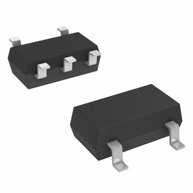
| 产品图片 |
|
| rohs | 符合RoHS无铅 / 符合限制有害物质指令(RoHS)规范要求 |
| 产品系列 | 板上安装温度传感器,Texas Instruments LM19CIZ/NOPB- |
| 数据手册 | |
| 产品型号 | LM19CIZ/NOPB |
| 产品目录页面 | |
| 产品种类 | 板上安装温度传感器 |
| 供应商器件封装 | TO-92-3 |
| 其它名称 | *LM19CIZ |
| 准确性 | +/- 3.8 C |
| 制造商产品页 | http://www.ti.com/general/docs/suppproductinfo.tsp?distId=10&orderablePartNumber=LM19CIZ/NOPB |
| 包装 | 散装 |
| 商标 | Texas Instruments |
| 封装 | Bulk |
| 封装/外壳 | TO-226-3、TO-92-3 标准主体 |
| 封装/箱体 | TO-92-3 |
| 工厂包装数量 | 1800 |
| 感应温度 | -55°C ~ 130°C |
| 标准包装 | 1,800 |
| 电压-电源 | 2.4 V ~ 5.5 V |
| 电源电流 | 4.5 uA |
| 精度 | ±2.5°C |
| 系列 | LM19 |
| 输出类型 | 电压 |


- 商务部:美国ITC正式对集成电路等产品启动337调查
- 曝三星4nm工艺存在良率问题 高通将骁龙8 Gen1或转产台积电
- 太阳诱电将投资9.5亿元在常州建新厂生产MLCC 预计2023年完工
- 英特尔发布欧洲新工厂建设计划 深化IDM 2.0 战略
- 台积电先进制程称霸业界 有大客户加持明年业绩稳了
- 达到5530亿美元!SIA预计今年全球半导体销售额将创下新高
- 英特尔拟将自动驾驶子公司Mobileye上市 估值或超500亿美元
- 三星加码芯片和SET,合并消费电子和移动部门,撤换高东真等 CEO
- 三星电子宣布重大人事变动 还合并消费电子和移动部门
- 海关总署:前11个月进口集成电路产品价值2.52万亿元 增长14.8%


PDF Datasheet 数据手册内容提取
LM19 www.ti.com SNIS122E–MAY2001–REVISEDMARCH2013 LM19 2.4V, 10µA, TO-92 Temperature Sensor CheckforSamples:LM19 FEATURES DESCRIPTION 1 • RatedforFull−55°Cto+130°CRange The LM19 is a precision analog output CMOS 2 integrated-circuit temperature sensor that operates • AvailableinaTO-92Package over a −55°C to +130°C temperature range. The • PredictableCurvatureError power supply operating range is +2.4 V to +5.5 V. • SuitableforRemoteApplications The transfer function of LM19 is predominately linear, yet has a slight predictable parabolic curvature. The • ULRecognizedComponent accuracy of the LM19 when specified to a parabolic transfer function is ±2.5°C at an ambient temperature APPLICATIONS of +30°C. The temperature error increases linearly • CellularPhones and reaches a maximum of ±3.8°C at the temperature range extremes. The temperature range • Computers is affected by the power supply voltage. At a power • PowerSupplyModules supply voltage of 2.7 V to 5.5 V the temperature • BatteryManagement range extremes are +130°C and −55°C. Decreasing the power supply voltage to 2.4 V changes the • FAXMachines negative extreme to −30°C, while the positive • Printers remainsat+130°C. • HVAC The LM19's quiescent current is less than 10 μA. • DiskDrives Therefore, self-heating is less than 0.02°C in still air. • Appliances Shutdown capability for the LM19 is intrinsic because its inherent low power consumption allows it to be KEY SPECIFICATIONS powered directly from the output of many logic gates ordoesnotnecessitateshutdownatall. • Accuracyat+30°C±2.5°C(max) • Accuracyat+130°C&−55°C±3.5to±3.8°C (max) • PowerSupplyVoltageRange+2.4Vto+5.5V • CurrentDrain10μA(max) • Nonlinearity±0.4%(typ) • OutputImpedance160Ω (max) • LoadRegulation – 0µA <I <+16 µA L 1 Pleasebeawarethatanimportantnoticeconcerningavailability,standardwarranty,anduseincriticalapplicationsof TexasInstrumentssemiconductorproductsanddisclaimerstheretoappearsattheendofthisdatasheet. Alltrademarksarethepropertyoftheirrespectiveowners. 2 PRODUCTIONDATAinformationiscurrentasofpublicationdate. Copyright©2001–2013,TexasInstrumentsIncorporated Products conform to specifications per the terms of the Texas Instruments standard warranty. Production processing does not necessarilyincludetestingofallparameters.
LM19 SNIS122E–MAY2001–REVISEDMARCH2013 www.ti.com Typical Application OutputVoltagevsTemperature V =(−3.88×10⁻⁶×T2)+(−1.15×10⁻²×T)+1.8639 O or where: Tistemperature,andV isthemeasuredoutputvoltageofthe O LM19. Figure1. Full-RangeCelsius(Centigrade)TemperatureSensor(−55°Cto+130°C)Operatingfroma SingleLi-IonBatteryCell Temperature(T) TypicalV O +130°C +303mV +100°C +675mV +80°C +919mV +30°C +1515mV +25°C +1574mV 0°C +1863.9mV −30°C +2205mV −40°C +2318mV −55°C +2485mV Connection Diagram Figure2. TO-92 PackageNumberLP Thesedeviceshavelimitedbuilt-inESDprotection.Theleadsshouldbeshortedtogetherorthedeviceplacedinconductivefoam duringstorageorhandlingtopreventelectrostaticdamagetotheMOSgates. 2 SubmitDocumentationFeedback Copyright©2001–2013,TexasInstrumentsIncorporated ProductFolderLinks:LM19
LM19 www.ti.com SNIS122E–MAY2001–REVISEDMARCH2013 Absolute Maximum Ratings(1) SupplyVoltage +6.5Vto−0.2V OutputVoltage (V++0.6V)to−0.6V OutputCurrent 10mA InputCurrentatanypin(2) 5mA StorageTemperature −65°Cto+150°C MaximumJunctionTemperature(T ) +150°C JMAX ESDSusceptibility(3) HumanBodyModel 2500V MachineModel 250V LeadTemperature TO-92Package Soldering(3secondsdwell) +240°C (1) AbsoluteMaximumRatingsindicatelimitsbeyondwhichdamagetothedevicemayoccur.OperatingRatingsindicateconditionsfor whichthedeviceisfunctional,butdonotensurespecificperformancelimits.Forensuredspecificationsandtestconditions,seethe ElectricalCharacteristics.Thespecifiedspecificationsapplyonlyforthetestconditionslisted.Someperformancecharacteristicsmay degradewhenthedeviceisnotoperatedunderthelistedtestconditions. (2) Whentheinputvoltage(V)atanypinexceedspowersupplies(V <GNDorV >V+),thecurrentatthatpinshouldbelimitedto5mA. I I I (3) Thehumanbodymodelisa100pFcapacitordischargedthrougha1.5kΩresistorintoeachpin.Themachinemodelisa200pF capacitordischargeddirectlyintoeachpin. Operating Ratings(1) SpecifiedTemperatureRange T ≤T ≤T MIN A MAX 2.4V≤V+≤2.7V −30°C≤T ≤+130°C A 2.7V≤V+≤5.5V −55°C≤T ≤+130°C A SupplyVoltageRange(V+) +2.4Vto+5.5V ThermalResistance,θ (2) TO-92 150°C/W JA (1) AbsoluteMaximumRatingsindicatelimitsbeyondwhichdamagetothedevicemayoccur.OperatingRatingsindicateconditionsfor whichthedeviceisfunctional,butdonotensurespecificperformancelimits.Forensuredspecificationsandtestconditions,seethe ElectricalCharacteristics.Thespecifiedspecificationsapplyonlyforthetestconditionslisted.Someperformancecharacteristicsmay degradewhenthedeviceisnotoperatedunderthelistedtestconditions. (2) Thejunctiontoambientthermalresistance(θ )isspecifiedwithoutaheatsinkinstillair. JA Copyright©2001–2013,TexasInstrumentsIncorporated SubmitDocumentationFeedback 3 ProductFolderLinks:LM19
LM19 SNIS122E–MAY2001–REVISEDMARCH2013 www.ti.com Electrical Characteristics Unlessotherwisenoted,thesespecificationsapplyforV+=+2.7V .BoldfacelimitsapplyforT =T =T toT ;all DC A J MIN MAX otherlimitsT =T =25°C;Unlessotherwisenoted. A J Parameter Conditions Typical(1) LM19C Units Limits(2) (Limit) TemperaturetoVoltageError T =+25°Cto+30°C ±2.5 °C(max) A V =(−3.88×10⁻⁶×T2) O T =+130°C ±3.5 °C(max) +(−1.15×10⁻²×T)+1.8639V(3) A T =+125°C ±3.5 °C(max) A T =+100°C ±3.2 °C(max) A T =+85°C ±3.1 °C(max) A T =+80°C ±3.0 °C(max) A T =0°C ±2.9 °C(max) A T =−30°C ±3.3 °C(min) A T =−40°C ±3.5 °C(max) A T =−55°C ±3.8 °C(max) A OutputVoltageat0°C +1.8639 V VariancefromCurve ±1.0 °C Non-Linearity(4) −20°C≤T ≤+80°C ±0.4 % A SensorGain(TemperatureSensitivity −30°C≤T ≤+100°C −11.77 −11.0 mV/°C(min) A orAverageSlope)toequation: −12.6 mV/°C(max) V =−11.77mV/°C×T+1.860V O OutputImpedance 0μA≤I ≤+16μA(5)(6) 160 Ω(max) L LoadRegulation(7) 0μA≤I ≤+16μA(5)(6) −2.5 mV(max) L LineRegulation(8) +2.4V≤V+≤+5.0V +3.7 mV/V(max) +5.0V≤V+≤+5.5V +11 mV(max) QuiescentCurrent +2.4V≤V+≤+5.0V 4.5 7 μA(max) +5.0V≤V+≤+5.5V 4.5 9 μA(max) +2.4V≤V+≤+5.0V 4.5 10 μA(max) ChangeofQuiescentCurrent +2.4V≤V+≤+5.5V +0.7 μA TemperatureCoefficientofQuiescent −11 nA/°C Current ShutdownCurrent V+≤+0.8V 0.02 μA (1) TypicalsareatT =T =25°Candrepresentmostlikelyparametricnorm. J A (2) LimitsareensuredtoAOQL(AverageOutgoingQualityLevel). (3) Accuracyisdefinedastheerrorbetweenthemeasuredandcalculatedoutputvoltageatthespecifiedconditionsofvoltage,current,and temperature(expressedin°C). (4) Non-Linearityisdefinedasthedeviationofthecalculatedoutput-voltage-versus-temperaturecurvefromthebest-fitstraightline,over thetemperaturerangespecified. (5) NegativecurrentsareflowingintotheLM19.PositivecurrentsareflowingoutoftheLM19.UsingthisconventiontheLM19canatmost sink−1μAandsource+16μA. (6) Loadregulationoroutputimpedancespecificationsapplyoverthesupplyvoltagerangeof+2.4Vto+5.5V. (7) Regulationismeasuredatconstantjunctiontemperature,usingpulsetestingwithalowdutycycle.Changesinoutputduetoheating effectscanbecomputedbymultiplyingtheinternaldissipationbythethermalresistance. (8) Lineregulationiscalculatedbysubtractingtheoutputvoltageatthehighestsupplyinputvoltagefromtheoutputvoltageatthelowest supplyinputvoltage. 4 SubmitDocumentationFeedback Copyright©2001–2013,TexasInstrumentsIncorporated ProductFolderLinks:LM19
LM19 www.ti.com SNIS122E–MAY2001–REVISEDMARCH2013 Typical Performance Characteristics TemperatureErrorvs.Temperature ThermalResponseinStillAir 5 4 MAX Limit 3 2 C) Typical º 1 R ( 0 O R R -1 E -2 MIN Limit -3 -4 -5 -100 -50 0 50 100 150 TEMPERATURE (ºC) LM19 TRANSFER FUNCTION The LM19's transfer function can be described in different ways with varying levels of precision. A simple linear transferfunction,withgoodaccuracynear25°C,is V =−11.69mV/°C×T+1.8663V (1) O Over the full operating temperature range of −55°C to +130°C, best accuracy can be obtained by using the parabolictransferfunction V =(−3.88×10⁻⁶×T2)+(−1.15×10⁻²×T)+1.8639 (2) O solvingforT: (3) Alineartransferfunctioncanbeusedoveralimitedtemperaturerangebycalculatingaslopeandoffsetthatgive best results over that range. A linear transfer function can be calculated from the parabolic transfer function of theLM19.Theslopeofthelineartransferfunctioncanbecalculatedusingthefollowingequation: m=−7.76×10⁻⁶×T−0.0115 where • TisthemiddleofthetemperaturerangeofinterestandmisinV/°C. (4) ForexampleforthetemperaturerangeofT =−30toT =+100°C: min max T=35°C and m=−11.77mV/°C Theoffsetofthelineartransferfunctioncanbecalculatedusingthefollowingequation: b=(V (T )+V (T)−m×(T +T))/2 OP max OP max where • V (T )isthecalculatedoutputvoltageatT usingtheparabolictransferfunctionforV . OP max max O • V (T)isthecalculatedoutputvoltageatTusingtheparabolictransferfunctionforV . (5) OP O Using this procedure the best fit linear transfer function for many popular temperature ranges was calculated in Table 1. As shown in Table 1 the error that is introduced by the linear transfer function increases with wider temperatureranges. Copyright©2001–2013,TexasInstrumentsIncorporated SubmitDocumentationFeedback 5 ProductFolderLinks:LM19
LM19 SNIS122E–MAY2001–REVISEDMARCH2013 www.ti.com Table1.FirstOrderEquationsOptimizedForDifferentTemperatureRanges TemperatureRange LinearEquation MaximumDeviationofLinearEquationfrom V = ParabolicEquation(°C) T (°C) T (°C) O min max −55 +130 −11.79mV/°C×T+1.8528V ±1.41 −40 +110 −11.77mV/°C×T+1.8577V ±0.93 −30 +100 −11.77mV/°C×T+1.8605V ±0.70 -40 +85 −11.67mV/°C×T+1.8583V ±0.65 −10 +65 −11.71mV/°C×T+1.8641V ±0.23 +35 +45 −11.81mV/°C×T+1.8701V ±0.004 +20 +30 −11.69mV/°C×T+1.8663V ±0.004 Mounting The LM19 can be applied easily in the same way as other integrated-circuit temperature sensors. It can be glued or cemented to a surface. The temperature that the LM19 is sensing will be within about +0.02°C of the surface temperaturetowhichtheLM19'sleadsareattached. This presumes that the ambient air temperature is almost the same as the surface temperature; if the air temperature were much higher or lower than the surface temperature, the actual temperature measured would beatanintermediatetemperaturebetweenthesurfacetemperatureandtheairtemperature. To ensure good thermal conductivity the backside of the LM19 die is directly attached to the GND pin. The tempertures of the lands and traces to the other leads of the LM19 will also affect the temperature that is being sensed. Alternatively, the LM19 can be mounted inside a sealed-end metal tube, and can then be dipped into a bath or screwed into a threaded hole in a tank. As with any IC, the LM19 and accompanying wiring and circuits must be kept insulated and dry, to avoid leakage and corrosion. This is especially true if the circuit may operate at cold temperatures where condensation can occur. Printed-circuit coatings and varnishes such as Humiseal and epoxy paintsordipsareoftenusedtoensurethatmoisturecannotcorrodetheLM19oritsconnections. The thermal resistance junction to ambient (θ ) is the parameter used to calculate the rise of a device junction JA temperature due to its power dissipation. For the LM19 the equation used to calculate the rise in the die temperatureisasfollows: T =T +θ [(V+I )+(V+−V )I ] J A JA Q O L where • I isthequiescentcurrentandI istheloadcurrentontheoutput. (6) Q L Since the LM19's junction temperature is the actual temperature being measured care should be taken to minimizetheloadcurrentthattheLM19isrequiredtodrive. Table 2 summarizes the rise in die temperature of the LM19 without any loading, and the thermal resistance for differentconditions. Table2.TemperatureRiseofLM19DuetoSelf-HeatingandThermalResistance(θ ) JA TO-92 TO-92 noheatsink smallheatfin θ T −T θ T −T JA J A JA J A (°C/W) (°C) (°C/W) (°C) Stillair 150 TBD TBD TBD Movingair TBD TBD TBD TBD 6 SubmitDocumentationFeedback Copyright©2001–2013,TexasInstrumentsIncorporated ProductFolderLinks:LM19
LM19 www.ti.com SNIS122E–MAY2001–REVISEDMARCH2013 Capacitive Loads The LM19 handles capacitive loading well. Without any precautions, the LM19 can drive any capacitive load less than 300 pF as shown in Figure 3. Over the specified temperature range the LM19 has a maximum output impedance of 160 Ω. In an extremely noisy environment it may be necessary to add some filtering to minimize noise pickup. It is recommended that 0.1 μF be added from V+ to GND to bypass the power supply voltage, as showninFigure4.Inanoisyenvironmentitmayevenbenecessarytoaddacapacitorfromtheoutputtoground with a series resistor as shown in Figure 4. A 1 μF output capacitor with the 160 Ω maximum output impedance and a 200 Ω series resistor will form a 442 Hz lowpass filter. Since the thermal time constant of the LM19 is muchslower,theoverallresponsetimeoftheLM19willnotbesignificantlyaffected. Figure3. LM19NoDecouplingRequiredforCapacitiveLoadsLessthan300pF Table3.LM19withFilterforNoisyEnvironment andCapacitiveLoadinggreaterthan300pF R(Ω) C(µF) 200 1 470 0.1 680 0.01 1k 0.001 Eitherplacementofresistorasshown aboveisjustaseffective. Figure4. LM19withFilterforNoisyEnvironment andCapacitiveLoadinggreaterthan300pF Copyright©2001–2013,TexasInstrumentsIncorporated SubmitDocumentationFeedback 7 ProductFolderLinks:LM19
LM19 SNIS122E–MAY2001–REVISEDMARCH2013 www.ti.com Applications Circuits V+ R3 VTEMP VT1 R4 VT2 4.1V R1 VT (High = overtemp alarm) +U1 VOUT VOUT LM4040 U3 0.1 PF - R2 LM7211 (4.1)R2 VT1= R2 + R1||R3 V+ LM19 VTemp (4.1)R2||R3 U2 VT2= R1 + R2||R3 Figure5. CentigradeThermostat Figure6. ConservingPowerDissipationwithShutdown Figure7. SuggestedConnectiontoaSamplingAnalogtoDigitalConverterInputStage Most CMOS ADCs found in ASICs have a sampled data comparator input structure that is notorious for causing grieftoanalogoutputdevicessuchastheLM19andmanyopamps.Thecauseofthisgriefistherequirementof instantaneous charge of the input sampling capacitor in the ADC. This requirement is easily accommodated by the addition of a capacitor. Since not all ADCs have identical input stages, the charge requirements will vary necessitating a different value of compensating capacitor. This ADC is shown as an example only. If a digital outputtemperatureisrequiredpleaserefertodevicessuchastheLM74. 8 SubmitDocumentationFeedback Copyright©2001–2013,TexasInstrumentsIncorporated ProductFolderLinks:LM19
LM19 www.ti.com SNIS122E–MAY2001–REVISEDMARCH2013 REVISION HISTORY ChangesfromRevisionD(March2013)toRevisionE Page • ChangedlayoutofNationalDataSheettoTIformat............................................................................................................ 8 Copyright©2001–2013,TexasInstrumentsIncorporated SubmitDocumentationFeedback 9 ProductFolderLinks:LM19
PACKAGE OPTION ADDENDUM www.ti.com 6-Feb-2020 PACKAGING INFORMATION Orderable Device Status Package Type Package Pins Package Eco Plan Lead/Ball Finish MSL Peak Temp Op Temp (°C) Device Marking Samples (1) Drawing Qty (2) (6) (3) (4/5) LM19CIZ/LFT4 ACTIVE TO-92 LP 3 2000 Green (RoHS SN N / A for Pkg Type LM19 & no Sb/Br) CIZ LM19CIZ/NOPB ACTIVE TO-92 LP 3 1800 Green (RoHS SN N / A for Pkg Type -55 to 130 LM19 & no Sb/Br) CIZ (1) The marketing status values are defined as follows: ACTIVE: Product device recommended for new designs. LIFEBUY: TI has announced that the device will be discontinued, and a lifetime-buy period is in effect. NRND: Not recommended for new designs. Device is in production to support existing customers, but TI does not recommend using this part in a new design. PREVIEW: Device has been announced but is not in production. Samples may or may not be available. OBSOLETE: TI has discontinued the production of the device. (2) RoHS: TI defines "RoHS" to mean semiconductor products that are compliant with the current EU RoHS requirements for all 10 RoHS substances, including the requirement that RoHS substance do not exceed 0.1% by weight in homogeneous materials. Where designed to be soldered at high temperatures, "RoHS" products are suitable for use in specified lead-free processes. TI may reference these types of products as "Pb-Free". RoHS Exempt: TI defines "RoHS Exempt" to mean products that contain lead but are compliant with EU RoHS pursuant to a specific EU RoHS exemption. Green: TI defines "Green" to mean the content of Chlorine (Cl) and Bromine (Br) based flame retardants meet JS709B low halogen requirements of <=1000ppm threshold. Antimony trioxide based flame retardants must also meet the <=1000ppm threshold requirement. (3) MSL, Peak Temp. - The Moisture Sensitivity Level rating according to the JEDEC industry standard classifications, and peak solder temperature. (4) There may be additional marking, which relates to the logo, the lot trace code information, or the environmental category on the device. (5) Multiple Device Markings will be inside parentheses. Only one Device Marking contained in parentheses and separated by a "~" will appear on a device. If a line is indented then it is a continuation of the previous line and the two combined represent the entire Device Marking for that device. (6) Lead/Ball Finish - Orderable Devices may have multiple material finish options. Finish options are separated by a vertical ruled line. Lead/Ball Finish values may wrap to two lines if the finish value exceeds the maximum column width. Important Information and Disclaimer:The information provided on this page represents TI's knowledge and belief as of the date that it is provided. TI bases its knowledge and belief on information provided by third parties, and makes no representation or warranty as to the accuracy of such information. Efforts are underway to better integrate information from third parties. TI has taken and continues to take reasonable steps to provide representative and accurate information but may not have conducted destructive testing or chemical analysis on incoming materials and chemicals. TI and TI suppliers consider certain information to be proprietary, and thus CAS numbers and other limited information may not be available for release. In no event shall TI's liability arising out of such information exceed the total purchase price of the TI part(s) at issue in this document sold by TI to Customer on an annual basis. Addendum-Page 1
PACKAGE OPTION ADDENDUM www.ti.com 6-Feb-2020 Addendum-Page 2
None
PACKAGE OUTLINE LP0003A TO-92 - 5.34 mm max height SCALE 1.200 SCALE 1.200 TO-92 5.21 4.44 EJECTOR PIN OPTIONAL 5.34 4.32 (1.5) TYP (2.54) SEATING 2X NOTE 3 PLANE 4 MAX (0.51) TYP 6X 0.076 MAX SEATING PLANE 3X 12.7 MIN 0.43 2X 0.55 3X 3X 0.35 2.6 0.2 0.38 2X 1.27 0.13 FORMED LEAD OPTION OTHER DIMENSIONS IDENTICAL STRAIGHT LEAD OPTION TO STRAIGHT LEAD OPTION 2.67 3X 2.03 4.19 3.17 3 2 1 3.43 MIN 4215214/B 04/2017 NOTES: 1. All linear dimensions are in millimeters. Any dimensions in parenthesis are for reference only. Dimensioning and tolerancing per ASME Y14.5M. 2. This drawing is subject to change without notice. 3. Lead dimensions are not controlled within this area. 4. Reference JEDEC TO-226, variation AA. 5. Shipping method: a. Straight lead option available in bulk pack only. b. Formed lead option available in tape and reel or ammo pack. c. Specific products can be offered in limited combinations of shipping medium and lead options. d. Consult product folder for more information on available options. www.ti.com
EXAMPLE BOARD LAYOUT LP0003A TO-92 - 5.34 mm max height TO-92 FULL R TYP 0.05 MAX (1.07) ALL AROUND METAL 3X ( 0.85) HOLE TYP TYP 2X METAL (1.5) 2X (1.5) 2X SOLDER MASK OPENING 1 2 3 (R0.05) TYP 2X (1.07) (1.27) SOLDER MASK (2.54) OPENING LAND PATTERN EXAMPLE STRAIGHT LEAD OPTION NON-SOLDER MASK DEFINED SCALE:15X 0.05 MAX ( 1.4) 2X ( 1.4) ALL AROUND METAL TYP 3X ( 0.9) HOLE METAL 2X (R0.05) TYP 1 2 3 SOLDER MASK OPENING (2.6) SOLDER MASK OPENING (5.2) LAND PATTERN EXAMPLE FORMED LEAD OPTION NON-SOLDER MASK DEFINED SCALE:15X 4215214/B 04/2017 www.ti.com
TAPE SPECIFICATIONS LP0003A TO-92 - 5.34 mm max height TO-92 13.7 11.7 32 23 (2.5) TYP 0.5 MIN 16.5 15.5 11.0 9.75 8.5 8.50 19.0 17.5 2.9 6.75 3.7-4.3 TYP TYP 2.4 5.95 13.0 12.4 FOR FORMED LEAD OPTION PACKAGE 4215214/B 04/2017 www.ti.com
IMPORTANTNOTICEANDDISCLAIMER TI PROVIDES TECHNICAL AND RELIABILITY DATA (INCLUDING DATASHEETS), DESIGN RESOURCES (INCLUDING REFERENCE DESIGNS), APPLICATION OR OTHER DESIGN ADVICE, WEB TOOLS, SAFETY INFORMATION, AND OTHER RESOURCES “AS IS” AND WITH ALL FAULTS, AND DISCLAIMS ALL WARRANTIES, EXPRESS AND IMPLIED, INCLUDING WITHOUT LIMITATION ANY IMPLIED WARRANTIES OF MERCHANTABILITY, FITNESS FOR A PARTICULAR PURPOSE OR NON-INFRINGEMENT OF THIRD PARTY INTELLECTUAL PROPERTY RIGHTS. These resources are intended for skilled developers designing with TI products. You are solely responsible for (1) selecting the appropriate TI products for your application, (2) designing, validating and testing your application, and (3) ensuring your application meets applicable standards, and any other safety, security, or other requirements. These resources are subject to change without notice. TI grants you permission to use these resources only for development of an application that uses the TI products described in the resource. Other reproduction and display of these resources is prohibited. No license is granted to any other TI intellectual property right or to any third party intellectual property right. TI disclaims responsibility for, and you will fully indemnify TI and its representatives against, any claims, damages, costs, losses, and liabilities arising out of your use of these resources. TI’s products are provided subject to TI’s Terms of Sale (www.ti.com/legal/termsofsale.html) or other applicable terms available either on ti.com or provided in conjunction with such TI products. TI’s provision of these resources does not expand or otherwise alter TI’s applicable warranties or warranty disclaimers for TI products. Mailing Address: Texas Instruments, Post Office Box 655303, Dallas, Texas 75265 Copyright © 2020, Texas Instruments Incorporated