ICGOO在线商城 > 传感器,变送器 > 温度传感器 - 模拟和数字输出 > AD22100KT
 Datasheet下载
- 型号: AD22100KT
- 制造商: Analog
- 库位|库存: xxxx|xxxx
- 要求:
| 数量阶梯 | 香港交货 | 国内含税 |
| +xxxx | $xxxx | ¥xxxx |
查看当月历史价格
查看今年历史价格
AD22100KT产品简介:
ICGOO电子元器件商城为您提供AD22100KT由Analog设计生产,在icgoo商城现货销售,并且可以通过原厂、代理商等渠道进行代购。 AD22100KT价格参考¥19.76-¥25.00。AnalogAD22100KT封装/规格:温度传感器 - 模拟和数字输出, 温度传感器 模拟,本地 0°C ~ 100°C 22.5mV/°C TO-92-3。您可以下载AD22100KT参考资料、Datasheet数据手册功能说明书,资料中有AD22100KT 详细功能的应用电路图电压和使用方法及教程。
AD22100KT 是由 Analog Devices Inc. 生产的一款温度传感器,它能够提供模拟和数字输出。这种传感器在工业、汽车以及消费电子等多个领域有着广泛的应用。

 工业应用
在工业环境中,AD22100KT 可用于监测和控制各种设备的温度。例如,在电机驱动系统中,它可以实时监控电机温度,防止过热导致的故障。此外,它还可以应用于加热器、冷却系统等设备中,确保这些设备在安全的工作温度范围内运行。通过精确的温度测量,可以提高系统的可靠性和效率,减少维护成本。

 汽车应用
在汽车行业,AD22100KT 适用于发动机管理系统中的温度监测。它可以安装在发动机周围的关键位置,如进气歧管、排气系统或冷却液通道,以监控发动机的运行温度。这对于优化发动机性能、提高燃油效率以及延长发动机寿命至关重要。此外,该传感器还可以用于空调系统和电池管理系统中,确保车内环境舒适,并保障电动汽车电池的安全运行。

 消费电子产品
在消费电子产品方面,AD22100KT 可以用于笔记本电脑、智能手机和其他便携式设备中,帮助监控内部温度并触发散热机制。这有助于防止设备因过热而损坏,同时提升用户体验。例如,当检测到温度过高时,设备可以自动降低处理器频率或启动风扇进行降温。

 其他应用
除了上述领域,AD22100KT 还可以应用于医疗设备、家用电器(如冰箱、微波炉)以及其他需要精确温度控制的场合。其高精度和可靠性使得它成为许多应用场景的理想选择。

总之,AD22100KT 温度传感器凭借其模拟和数字输出功能,能够在多种复杂环境下提供可靠的温度监测,满足不同行业的需求。
| 参数 | 数值 |
| 产品目录 | |
| 描述 | IC TEMP SENSOR VOUT TO92-3板上安装温度传感器 VOUT TEMP SENSOR IC |
| 产品分类 | 温度传感器,变送器温度传感器 |
| 品牌 | Analog Devices Inc |
| 产品手册 | |
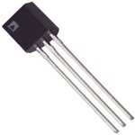
| 产品图片 |
|
| rohs | 否不符合限制有害物质指令(RoHS)规范要求 |
| 产品系列 | 板上安装温度传感器,Analog Devices AD22100KT- |
| 数据手册 | |
| 产品型号 | AD22100KT |
| 产品种类 | 板上安装温度传感器 |
| 供应商器件封装 | TO-92-3 |
| 准确性 | 0.5 C |
| 包装 | 管件 |
| 商标 | Analog Devices |
| 增益 | + 22.5 mV / C |
| 安装风格 | Through Hole |
| 封装 | Bulk |
| 封装/外壳 | TO-226-3、TO-92-3 标准主体 |
| 封装/箱体 | TO-92-3 |
| 工厂包装数量 | 100 |
| 感应温度 | 0°C ~ 100°C |
| 数字输出-总线接口 | - |
| 最大工作温度 | + 100 C |
| 最小工作温度 | 0 C |
| 标准包装 | 100 |
| 电压-电源 | 4 V ~ 6.5 V |
| 电源电压-最大 | 6.5 V |
| 电源电压-最小 | 4 V |
| 电源电流 | 500 uA |
| 精度 | ±0.5°C |
| 系列 | AD22100 |
| 设备功能 | Signal Conditioner |
| 输出类型 | 模拟,比率 |

,TO-226_straightlead.jpg)


- 商务部:美国ITC正式对集成电路等产品启动337调查
- 曝三星4nm工艺存在良率问题 高通将骁龙8 Gen1或转产台积电
- 太阳诱电将投资9.5亿元在常州建新厂生产MLCC 预计2023年完工
- 英特尔发布欧洲新工厂建设计划 深化IDM 2.0 战略
- 台积电先进制程称霸业界 有大客户加持明年业绩稳了
- 达到5530亿美元!SIA预计今年全球半导体销售额将创下新高
- 英特尔拟将自动驾驶子公司Mobileye上市 估值或超500亿美元
- 三星加码芯片和SET,合并消费电子和移动部门,撤换高东真等 CEO
- 三星电子宣布重大人事变动 还合并消费电子和移动部门
- 海关总署:前11个月进口集成电路产品价值2.52万亿元 增长14.8%


PDF Datasheet 数据手册内容提取
Voltage Output Temperature Sensor with Signal Conditioning AD22100 FUNCTIONAL BLOCK DIAGRAM FEATURES 200°C temperature span V+ Accuracy better than ±2% of full scale Linearity better than ±1% of full scale Temperature coefficient of 22.5 mV/°C Output proportional to temperature × V+ VOUT Single-supply operation RMeinveimrsael vsoellft-ahgeea ptirnogt ection RT 00673-C-001 High level, low impedance output Figure 1. APPLICATIONS HVAC systems +5V System temperature compensation Board level temperature sensing REFERENCE Electronic thermostats ANALOG-TO- DIGITAL MARKETS AD22100 SIGNAL OUTPUT CONVERTER Industrial process control VO DIRECT TO ADC INPUT Instrumentation 1k 0.1F Automotive GENERAL DESCRIPTION –50C TO +150C 00673-C-002 The AD22100 is a monolithic temperature sensor with on-chip Figure 2. Application Circuit signal conditioning. It can be operated over the temperature range −50°C to +150°C, making it ideal for use in numerous HVAC, instrumentation, and automotive applications. The signal conditioning eliminates the need for any trimming, buffering, or linearization circuitry, greatly simplifying the system design and reducing the overall system cost. The output voltage is proportional to the temperature x the supply voltage (ratiometric). The output swings from 0.25 V at −50°C to +4.75 V at +150°C using a single +5.0 V supply. Due to its ratiometric nature, the AD22100 offers a cost- effective solution when interfacing to an analog-to-digital converter. This is accomplished by using the ADC’s +5 V power supply as a reference to both the ADC and the AD22100 eliminating the need for and cost of a precision reference (see Figure 2). Rev. D Information furnished by Analog Devices is believed to be accurate and reliable. However, no responsibility is assumed by Analog Devices for its use, nor for any infringements of patents or other rights of third parties that may result from its use. One Technology Way, P.O. Box 9106, Norwood, MA 02062-9106, U.S.A. Specifications subject to change without notice. No license is granted by implication or otherwise under any patent or patent rights of Analog Devices. Trademarks and Tel: 781.329.4700 www.analog.com registered trademarks are the property of their respective owners. Fax: 781.326.8703 © 2004 Analog Devices, Inc. All rights reserved.
AD22100 TABLE OF CONTENTS Specifications.....................................................................................3 Output Stage Considerations.......................................................7 Chip Specifications.......................................................................3 Ratiometricity Considerations....................................................8 Absolute Maximum Ratings............................................................4 Mounting Considerations............................................................8 ESD Caution..................................................................................4 Thermal Environment Effects.....................................................8 Pin Configurations and Function Descriptions...........................5 Microprocessor A/D Interface Issues.........................................9 Typical Performance Characteristics.............................................6 Use with a Precision Reference as the Supply Voltage................9 Theory of Operation........................................................................7 Outline Dimensions.......................................................................10 Absolute Accuracy and Nonlinearity Specifications...............7 Ordering Guide..........................................................................11 REVISION HISTORY 7/04—Data Sheet Changed from Rev. C to Rev. D Change to AD22100K Specifications.............................................3 Updated Outline Dimensions.......................................................10 Changes to Ordering Guide..........................................................11 6/04—Data Sheet Changed from Rev. B to Rev. C Changes to Format.............................................................Universal Changes to Specifications................................................................3 Changes to Chip Specifications......................................................3 Changes to Ratiometricity Considerations Section.....................8 Changes to Ordering Guide..........................................................10 Updated Outline Dimensions.......................................................10 12/94—Data Sheet Changed from Rev. A to Rev. B Rev. D | Page 2 of 12
AD22100 SPECIFICATIONS T = 25°C and V+ = 4 V to 6.5 V, unless otherwise noted. A Table 1. AD22100K AD22100A AD22100S Parameter Min Typ Max Min Typ Max Min Typ Max Unit TRANSFER FUNCTION V = (V+/5 V) × [1.375 V +(22.5 mV/°C) × T ] V OUT A TEMPERATURE COEFFICIENT (V+/5 V) × 22.5 mV/°C TOTAL ERROR Initial Error T = 25°C ±0.5 ±2.0 ±1.0 ±2.0 ±1.0 ±2.0 °C A Error Overtemperature T = T ±0.75 ±2.0 ±2.0 ±3.7 ±3.0 ±4.0 °C A MIN T = T ±0.75 ±2.0 ±2.0 ±3.0 ±3.0 ±4.0 °C A MAX Nonlinearity T = T to T 0.5 0.5 1.0 % FS1 A MAX MIN OUTPUT CHARACTERISTICS Nominal Output Voltage V+ = 5.0 V, T = 0°C 1.375 V A V+ = 5.0 V, T = +100°C 3.625 V A V+ = 5.0 V, T = −40°C 0.475 V A V+ = 5.0 V, T = +85°C 3.288 V A V+ = 5.0 V, T = −50°C 0.250 V A V+ = 5.0 V, T = +150°C 4.750 V A POWER SUPPLY Operating Voltage 4.0 5.0 6.5 4.0 5.0 6.5 4.0 5.0 6.5 V Quiescent Current 500 650 500 650 500 650 µA TEMPERATURE RANGE Guaranteed Temperature Range 0 +100 −40 +85 −50 +150 °C Operating Temperature Range −50 +150 −50 +150 −50 +150 °C PACKAGE TO-92 TO-92 TO-92 SOIC SOIC SOIC 1 FS (full scale) is defined as the operating temperature range −50°C to +150°C. The listed maximum specification limit applies to the guaranteed temperature range. For example, the AD22100K has a nonlinearity of (0.5%) × (200°C) = 1°C over the guaranteed temperature range of 0°C to +100°C. CHIP SPECIFICATIONS T = 25°C and V+ = 5.0 V, unless otherwise noted. A Table 2. Paramater Min Typ Max Unit TRANSFER FUNCTION V = (V+/5 V) × [1.375 V +(22.5 mV/°C) × T ] V OUT A TEMPERATURE COEFFICIENT (V+/5 V) × 22.5 mV/°C OUTPUT CHARACTERISTICS Error T = 25°C ±0.5 ±2.0 °C A Nominal Output Voltage T = 25°C 1.938 V A POWER SUPPLY Operating Voltage 4.0 5.0 6.5 V Quiescent Current 500 650 µA TEMPERATURE RANGE Guaranteed Temperature Range +25 °C Operating Temperature Range −50 +150 °C Rev. D | Page 3 of 12
AD22100 ABSOLUTE MAXIMUM RATINGS Table 3. Parameter Rating Supply Voltage 10 V Stresses above those listed under Absolute Maximum Ratings Reversed Continuous Supply Voltage −10 V may cause permanent damage to the device. This is a stress Operating Temperature –50°C to +150°C rating only and functional operation of the device at these or Storage Temperature –65°C to +160°C any other conditions above those indicated in the operational Output Short Circuit to V+ or Ground Indefinite section of this specification is not implied. Exposure to absolute Lead Temperature Range 300°C maximum rating conditions for extended periods may affect (Soldering 10 sec) device reliability. Junction Temperature 150°C ESD CAUTION ESD (electrostatic discharge) sensitive device. Electrostatic charges as high as 4000 V readily accumulate on the human body and test equipment and can discharge without detection. Although this product features proprietary ESD protection circuitry, permanent damage may occur on devices subjected to high energy electrostatic discharges. Therefore, proper ESD precautions are recommended to avoid performance degradation or loss of functionality. Rev. D | Page 4 of 12
AD22100 PIN CONFIGURATIONS AND FUNCTION DESCRIPTIONS VO V+ 1 8 NC V+ GND VO 2 AD22100 7 NC 1 2 3 NC 3 TOP VIEW 6 NC B(ONToTt OtoM S VcaIEleW) 00673-C-003 GND N4C( =N oNtO to C SOcNaNleE)CT5 NC 00673-C-004 Figure 4. 8-Lead SOIC Figure 3. 3-Lead TO-92 Table 4. 3-Lead TO-92 Pin Function Descriptions Table 5. 8-Lead SOIC Pin Function Descriptions Pin No. Mnemonic Description Pin No. Mnemonic Description 1 V+ Power Supply Input. 1 V+ Power Supply Input. 2 VO Device Output. 2 VO Device Output. 3 GND Ground Pin Must Be Connected to 0 V. 3 NC No Connect. 4 GND Ground Pin Must Be Connected to 0 V. 5 NC No Connect. 6 NC No Connect. 7 NC No Connect. 8 NC No Connect. Rev. D | Page 5 of 12
AD22100 TYPICAL PERFORMANCE CHARACTERISTICS 16 250 14 200 12 (SOIC) ec)10 T (T0-92) W) τ(S (C/°A150 8 θJ 6 100 24 T (SOIC) 00673-C-005 50 (T0-92) 00673-C-006 0 400 800 1200 0 400 800 1200 FLOW RATE (CFM) FLOW RATE (CFM) Figure 5. Thermal Response vs. Flow Rate Figure 6. Thermal Resistance vs. Flow Rate Rev. D | Page 6 of 12
AD22100 THEORY OF OPERATION The AD22100 is a ratiometric temperature sensor IC whose 4 output voltage is proportional to its power supply voltage. The 3 heart of the sensor is a proprietary temperature-dependent MAXIMUM ERROR resistor, similar to an RTD, which is built into the IC. Figure 7 2 OVER TEMPERATURE shows a functional block diagram of the AD22100. 1 C) V+ OR (° 0 R ER –1 TYPICAL ERROR –2 MAXIMUM ERROR OVER TEMPERATURE RT VOUT00673-C-001 ––43–50 0 TEMPERA50TURE(°C) 100 15000673-C-007 Figure 7. Simplified Block Diagram Figure 8. Typical AD22100 Performance The temperature-dependent resistor, labeled R , exhibits a OUTPUT STAGE CONSIDERATIONS T change in resistance that is nearly linearly proportional to As previously stated, the AD22100 is a voltage output device. A temperature. This resistor is excited with a current source that is basic understanding of the nature of its output stage is useful for proportional to the power supply voltage. The resulting voltage proper application. Note that at the nominal supply voltage of across R is therefore both supply voltage proportional and line- T 5.0 V, the output voltage extends from 0.25 V at –50°C to +4.75 arly varying with temperature. The remainder of the AD22100 V at +150°C. Furthermore, the AD22100 output pin is capable consists of an op amp signal conditioning block that takes the of withstanding an indefinite short circuit to either ground or voltage across R and applies the proper gain and offset to T the power supply. These characteristics are provided by the out- achieve the following output voltage function: put stage structure shown in Figure 9. V = (V+/5 V) × (1.375 V + 22.5 mV/°C × T ) OUT A V+ ABSOLUTE ACCURACY AND NONLINEARITY SPECIFICATIONS VOUT Figure 8 graphically depicts the guaranteed limits of accuracy fAsoesrt , t tfhhoeer oAinuDstpt2au2nt1c i0es0 ev raernroydr l sianht eoraworo,s m tthh etee mpmeaprjofeorrra smtouuarenr,cc eseps o aofnf a ee trryrrpoorirc, aaarlne pd oa fdrfte-. - 00673-C-008 Figure 9. Output Stage Structure viation from the theoretical 22.5 mV/°C. Demanding applica- tions can achieve improved performance by calibrating these The active portion of the output stage is a PNP transistor, offset and gain errors so that only the residual nonlinearity re- with its emitter connected to the V+ supply and its collector mains as a significant source of error. connected to the output node. This PNP transistor sources the required amount of output current. A limited pull-down capa- bility is provided by a fixed current sink of about −80 µA, with the term fixed referring to a current sink that is fairly insensitive to either supply voltage or output loading conditions. The cur- rent sink capability is a function of temperature, increasing its pull-down capability at lower temperatures. Rev. D | Page 7 of 12
AD22100 Due to its limited current sinking ability, the AD22100 is inca- MOUNTING CONSIDERATIONS pable of driving loads to the V+ power supply and is instead If the AD22100 is thermally attached and properly protected, it intended to drive grounded loads. A typical value for short- can be used in any measuring situation where the maximum circuit current limit is 7 mA, so devices can reliably source 1 range of temperatures encountered is between −50°C and mA or 2 mA. However, for best output voltage accuracy and +150°C. Because plastic IC packaging technology is employed, minimal internal self-heating, output current should be kept excessive mechanical stress must be avoided when fastening the below 1 mA. Loads connected to the V+ power supply should device with a clamp or screw-on heat tab. Thermally conductive be avoided as the current sinking capability of the AD22100 is epoxy or glue is recommended for typical mounting conditions. fairly limited. These considerations are typically not a problem In wet or corrosive environments, an electrically isolated metal when driving a microcontroller analog-to-digital converter input or ceramic well should be used to shield the AD22100. Because pin (see the Microprocessor A/D Interface Issues section). the part has a voltage output (as opposed to current), it offers modest immunity to leakage errors, such as those caused by RATIOMETRICITY CONSIDERATIONS condensation at low temperatures. The AD22100 will operate with slightly better accuracy than that listed in the data sheet specifications if the power supply is THERMAL ENVIRONMENT EFFECTS held constant. This is because the AD22100’s output voltage The thermal environment in which the AD22100 is used varies with both temperature and supply voltage, with some determines two performance traits: the effect of self-heating on errors. The ideal transfer function describing output voltage is: accuracy and the response time of the sensor to rapid changes in temperature. In the first case, a rise in the IC junction (V+/5 V) × (1.375 V + 22.5 mV/°C × T ) A temperature above the ambient temperature is a function of two The ratiometricity error is defined as the percent change away variables: the power consumption of the AD22100 and the from the ideal transfer function as the power supply voltage thermal resistance between the chip and the ambient environ- changes within the operating range of 4 V to 6.5 V. For the ment θ Self-heating error in °C can be derived by multiplying JA. AD22100, this error is typically less than 1%. A movement from the power dissipation by θ . Because errors of this type can JA the ideal transfer function by 1% at 25°C, with a supply voltage vary widely for surroundings with different heat-sinking capaci- varying from 5.0 V to 5.50 V, results in a 1.94 mV change in ties, it is necessary to specify θ under several conditions. Table JA output voltage or 0.08°C error. This error term is greater at 6 shows how the magnitude of self-heating error varies relative higher temperatures because the output (and error term) is to the environment. A typical part will dissipate about 2.2 mW directly proportional to temperature. At 150°C, the error in at room temperature with a 5 V supply and negligible output output voltage is 4.75 mV or 0.19°C. loading. Table 6 indicates a θ of 190°C/W in still air, without a JA heat sink, yielding a temperature rise of 0.4°C. Thermal rise will For example, with V = 5.0 V, and T = +25°C, the nominal S A be considerably less in either moving air or with direct physical output of the AD22100 will be 1.9375 V. At V = 5.50 V, the S connection to a solid (or liquid) body. nominal output will be 2.1313 V, an increase of 193.75 mV. A Table 6. Thermal Resistance (TO-92) proportionality error of 1% is applied to the 193.75 mV, yielding Medium θ (°C/W) t (sec)1 an error term of 1.9375 mV. This error term translates to a JA Aluminum Block 60 2 variation in output voltage of 2.1293 V to 2.3332 V. A 1.94 mV Moving Air2 error at the output is equivalent to about 0.08°C error in accuracy. Without Heat Sink 75 3.5 Still Air If 150°C is substituted for 25°C in the above example, the error Without Heat Sink 190 15 term translates to a variation in output voltage of 5.2203 V to 5.2298 V. A 4.75 mV error at the output is equivalent to about 0.19°C error in accuracy. Rev. D | Page 8 of 12
AD22100 Response of the AD22100 output to abrupt changes in ambient MICROPROCESSOR A/D INTERFACE ISSUES temperature can be modeled by a single time constant t expo- The AD22100 is especially well suited to providing a low cost nential function. Figure 10 shows the typical response time temperature measurement capability for microprocessor/ plots for a few media of interest. microcontroller based systems. Many inexpensive 8-bit micro- processors now offer an onboard 8-bit ADC capability at a 100 90 ALUMINUM modest cost premium. Total cost of ownership then becomes a BLOCK function of the voltage reference and analog signal conditioning 80 MOVING AIR necessary to mate the analog sensor with the microprocessor ES70 ADC. The AD22100 can provide an ideal low cost system by U AL60 STILL AIR eliminating the need for a precision voltage reference and any V AL 50 additional active components. The ratiometric nature of the N F FI40 AD22100 allows the microprocessor to use the same power O supply as its ADC reference. Variations of hundreds of mil- % 30 livolts in the supply voltage have little effect as both the 20 AD22100 and the ADC use the supply as their reference. The 100 00673-C-009 n+o1m50i°nCa)l AmDak2e2s1 g0o0o sdig unsael oraf nthgee oinf p0u.2t 5r aVn gtoe o4f.7 a5 0 V V ( −to5 05° VC to 0 10 20 30 40 50 60 70 80 90 100 TIME (sec) ADC. A single resistor and capacitor are recommended to pro- vide immunity to the high speed charge dump glitches seen at Figure 10. Response Time many microprocessor ADC inputs (see Figure 2). The time constant t is dependent on θ and the thermal capaci- JA ties of the chip and the package. Table 6 lists the effective t (time An 8-bit ADC with a reference of 5 V will have a least signifi- to reach 63.2% of the final value) for a few different media. cant bit (LSB) size of 5 V/256 = 19.5 mV. This corresponds to a Copper printed circuit board connections were neglected in the nominal resolution of about 0.87°C. analysis; however, they will sink or conduct heat directly USE WITH A PRECISION REFERENCE AS THE SUPPLY through the AD22100’s solder plated copper leads. When faster VOLTAGE response is required, a thermally conductive grease or glue between the AD22100 and the surface temperature being While the ratiometric nature of the AD22100 allows for system measured should be used. operation without a precision voltage reference, it can still be used in such systems. Overall system requirements involving other sensors or signal inputs may dictate the need for a fixed precision ADC reference. The AD22100 can be converted to absolute voltage operation by using a precision reference as the supply voltage. For example, a 5.00 V reference can be used to power the AD22100 directly. Supply current will typically be 500 µA, which is usually within the output capability of the reference. Using a large number of AD22100s may require an additional op amp buffer, as would scaling down a 10.00 V ref- erence that might be found in instrumentation ADCs typically operating from ±15 V supplies. 1 The time constant t is defined as the time to reach 63.2% of the final temperature change. 2 1200 CFM. Rev. D | Page 9 of 12
AD22100 OUTLINE DIMENSIONS 0.210 (5.33) 0.170 (4.32) 0.050 (1.27) 0.165 (4.19) MAX 0.125 (3.18) 0.205 (5.21) 0.019 (0.482)SQ 0.055 (1.40) 0.175 (4.45) 0.016 (0.407) 0.045 (1.15) 3 2 0.105 (2.66) 1 0.095 (2.42) 0.135 (3.43) 0.500 (12.70) MIN 0.115 (2.92) MIN SEATING 0.115 (2.92) 0.080 (2.03) PLANE 0.080 (2.03) BOTTOM VIEW COMPLIANT TO JEDEC STANDARDS TO-226AA CONTROLLING DIMENSIONS ARE IN INCHES; MILLIMETER DIMENSIONS (IN PARENTHESES) ARE ROUNDED-OFF EQUIVALENTS FOR REFERENCE ONLY AND ARE NOT APPROPRIATE FOR USE IN DESIGN Figure 11. 3-Pin Plastic Header Package [TO-92] (T-3) Dimensions shown in inches and millimeters 5.00(0.1968) 4.80(0.1890) 8 5 4.00 (0.1574) 6.20 (0.2440) 3.80 (0.1497) 1 4 5.80 (0.2284) 1.27 (0.0500) 0.50 (0.0196) BSC 1.75 (0.0688) 0.25 (0.0099)× 45° 0.25 (0.0098) 1.35 (0.0532) 0.10 (0.0040) 0.51 (0.0201) 8° COPL0A.1N0ARITY SEPALTAINNGE 0.31 (0.0122) 00..2157 ((00..00009687)) 0° 10..2470 ((00..00510507)) COMPLIANT TO JEDEC STANDARDS MS-012AA CONTROLLING DIMENSIONS ARE IN MILLIMETERS; INCH DIMENSIONS (IN PARENTHESES) ARE ROUNDED-OFF MILLIMETER EQUIVALENTS FOR REFERENCE ONLY AND ARE NOT APPROPRIATE FOR USE IN DESIGN Figure 12. 8-Lead Standard Small Outline Package [SOIC] (R-8) Dimensions shown in inches and millimeters Rev. D | Page 10 of 12
AD22100 ORDERING GUIDE Models Temperature Range Package Description Package Outline AD22100KT 0°C to +100°C 3-Pin Plastic Header Package (TO-92) T-3 AD22100KR 0°C to +100°C 8-Lead Standard Small Outline Package (SOIC) R-8 AD22100KR-REEL7 0°C to +100°C 8-Lead Standard Small Outline Package (SOIC) R-8 AD22100KRZ1 0°C to +100°C 8-Lead Standard Small Outline Package (SOIC) R-8 AD22100KRZ-REEL71 0°C to +100°C 8-Lead Standard Small Outline Package (SOIC) R-8 AD22100AT –40°C to +85°C 3-Pin Plastic Header Package (TO-92) T-3 AD22100AR –40°C to +85°C 8-Lead Standard Small Outline Package (SOIC) R-8 AD22100AR-REEL –40°C to +85°C 8-Lead Standard Small Outline Package (SOIC) R-8 AD22100AR-REEL7 –40°C to +85°C 8-Lead Standard Small Outline Package (SOIC) R-8 AD22100ST –50°C to +150°C 3-Pin Plastic Header Package (TO-92) T-3 AD22100SR –50°C to +150°C 8-Lead Standard Small Outline Package (SOIC) R-8 AD22100SR-REEL7 –50°C to +150°C 8-Lead Standard Small Outline Package (SOIC) R-8 AD22100SRZ1 –50°C to +150°C 8-Lead Standard Small Outline Package (SOIC) R-8 AD22100SRZ-REEL71 –50°C to +150°C 8-Lead Standard Small Outline Package (SOIC) R-8 AD22100KCHIPS DIE 1 Z = Pb-free part. Rev. D | Page 11 of 12
AD22100 NOTES © 2004 Analog Devices, Inc. All rights reserved. Trademarks and regis- tered trademarks are the property of their respective owners. C00673–0–7/04(D) Rev. D | Page 12 of 12