ICGOO在线商城 > 传感器,变送器 > 温度传感器 - 模拟和数字输出 > TCN75AVOA

 Datasheet下载
- 型号: TCN75AVOA
- 制造商: Microchip
- 库位|库存: xxxx|xxxx
- 要求:
| 数量阶梯 | 香港交货 | 国内含税 |
| +xxxx | $xxxx | ¥xxxx |
查看当月历史价格
查看今年历史价格
TCN75AVOA产品简介:
ICGOO电子元器件商城为您提供TCN75AVOA由Microchip设计生产,在icgoo商城现货销售,并且可以通过原厂、代理商等渠道进行代购。 TCN75AVOA价格参考¥4.63-¥4.63。MicrochipTCN75AVOA封装/规格:温度传感器 - 模拟和数字输出, 温度传感器 数字,本地 -55°C ~ 125°C 11 b 8-SOIC。您可以下载TCN75AVOA参考资料、Datasheet数据手册功能说明书,资料中有TCN75AVOA 详细功能的应用电路图电压和使用方法及教程。
Microchip Technology的TCN75AVOA是一款高精度、低功耗的数字温度传感器,适用于多种应用场景。该器件采用I²C接口,支持SMBus兼容通信协议,具有12位分辨率,能够在-55°C至+125°C的宽温度范围内提供精确的温度测量。其典型应用场景包括但不限于以下几类:

 1. 工业自动化与控制
   TCN75AVOA可用于工业设备中的温度监控,如电机、变频器、PLC(可编程逻辑控制器)等。它能够实时监测环境温度或关键部件的温度变化,确保设备在安全温度范围内运行,避免过热损坏。此外,该传感器还支持报警功能,当温度超过预设阈值时,可以通过I²C接口向主控系统发送警告信号。

 2. 消费电子
   在消费电子产品中,如笔记本电脑、智能手机和平板电脑等,TCN75AVOA可以用于监控内部温度,防止过热导致性能下降或硬件损坏。它还可以用于智能家电,如冰箱、空调等,帮助调节温度并优化能耗。

 3. 医疗设备
   医疗设备对温度的精确控制要求较高,TCN75AVOA可以应用于便携式医疗设备、监护仪、血液分析仪等,确保设备在稳定的工作温度下运行,从而保证测量结果的准确性。此外,它还可以用于医院的环境监控系统,确保病房和实验室的温度符合标准。

 4. 汽车电子
   在汽车电子系统中,TCN75AVOA可用于监控电池管理系统(BMS)、发动机舱内的温度以及车内环境温度。特别是在电动汽车中,电池温度的精确监控对于确保电池的安全性和延长使用寿命至关重要。该传感器的低功耗特性也使其适合长时间运行的车载应用。

 5. 服务器与数据中心
   数据中心的服务器、交换机等设备需要严格的温度监控,以防止过热影响性能或导致硬件故障。TCN75AVOA可以集成到服务器主板或其他关键组件中,提供实时温度反馈,帮助管理员进行散热管理,确保系统的稳定运行。

总之,TCN75AVOA凭借其高精度、低功耗和灵活的通信接口,广泛适用于各种需要精确温度监控的应用场景。
| 参数 | 数值 |
| 产品目录 | 集成电路 (IC)热管理产品 |
| 描述 | IC TEMP SENSOR SRL 2.7V 8SOIC板上安装温度传感器 2-Wire SER Temp Sens/Ther Mon |
| 产品分类 | |
| 品牌 | Microchip Technology |
| 产品手册 | |
| 产品图片 |
|
| rohs | 符合RoHS无铅 / 符合限制有害物质指令(RoHS)规范要求 |
| 产品系列 | 板上安装温度传感器,Microchip Technology TCN75AVOA- |
| 数据手册 | 点击此处下载产品Datasheethttp://www.microchip.com/mymicrochip/filehandler.aspx?ddocname=en022251http://www.microchip.com/mymicrochip/filehandler.aspx?ddocname=en531285http://www.microchip.com/mymicrochip/filehandler.aspx?ddocname=en023833 |
| 产品型号 | TCN75AVOA |
| PCN组件/产地 | http://www.microchip.com/mymicrochip/NotificationDetails.aspx?id=5774&print=view |
| PCN设计/规格 | http://www.microchip.com/mymicrochip/NotificationDetails.aspx?id=5576&print=viewhttp://www.microchip.com/mymicrochip/NotificationDetails.aspx?id=5704&print=view |
| 产品目录页面 | |
| 产品种类 | 板上安装温度传感器 |
| 传感器类型 | 内部 |
| 供应商器件封装 | 8-SOIC N |
| 关闭 | Shutdown |
| 准确性 | +/- 2 C |
| 功能 | 温度监控系统(传感器) |
| 包装 | 管件 |
| 商标 | Microchip Technology |
| 安装类型 | 表面贴装 |
| 安装风格 | SMD/SMT |
| 封装 | Tube |
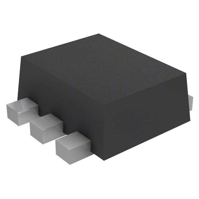
| 封装/外壳 | 8-SOIC(0.154",3.90mm 宽) |
| 封装/箱体 | SOIC-8 |
| 工作温度 | -55°C ~ 125°C |
| 工厂包装数量 | 100 |
| 感应温度 | -55°C ~ 125°C |
| 拓扑 | ADC(三角积分型),寄存器库 |
| 数字输出-位数 | 9 bit to 12 bit |
| 数字输出-总线接口 | 2-Wire, I2C, SMBus |
| 最大工作温度 | + 125 C |
| 最小工作温度 | - 55 C |
| 标准包装 | 100 |
| 温度阈值 | Programmable |
| 特色产品 | http://www.digikey.cn/product-highlights/zh/tcn75a-digital-temperature-sensor/50305 |
| 电压-电源 | 2.7 V ~ 5.5 V |
| 电源电压-最大 | 5.5 V |
| 电源电压-最小 | 2.7 V |
| 电源电流 | 500 uA |
| 精度 | ±3°C(最大) |
| 设备功能 | Sensor with Alert |
| 输出报警 | 无 |
| 输出电流 | 1 uA |
| 输出类型 | Digital |
| 输出风扇 | 是 |
| 配置 | Local |


- 商务部:美国ITC正式对集成电路等产品启动337调查
- 曝三星4nm工艺存在良率问题 高通将骁龙8 Gen1或转产台积电
- 太阳诱电将投资9.5亿元在常州建新厂生产MLCC 预计2023年完工
- 英特尔发布欧洲新工厂建设计划 深化IDM 2.0 战略
- 台积电先进制程称霸业界 有大客户加持明年业绩稳了
- 达到5530亿美元!SIA预计今年全球半导体销售额将创下新高
- 英特尔拟将自动驾驶子公司Mobileye上市 估值或超500亿美元
- 三星加码芯片和SET,合并消费电子和移动部门,撤换高东真等 CEO
- 三星电子宣布重大人事变动 还合并消费电子和移动部门
- 海关总署:前11个月进口集成电路产品价值2.52万亿元 增长14.8%


PDF Datasheet 数据手册内容提取
TCN75A 2-Wire Serial Temperature Sensor Features: Description: • Temperature-to-Digital Converter Microchip Technology Inc.’s TCN75A digital tempera- • Accuracy: ture sensor converts temperatures between -40°C and +125°C to a digital word, with ±1°C (typ.) accuracy. - ±1 (typ.) from -40°C to +125°C - ±2°C (max.) from +40°C to +125°C The TCN75A product comes with user-programmable registers that provide flexibility for temperature-sensing • User-selectable Resolution: 0.5°C to 0.0625°C applications. The register settings allow user-select- • Operating Voltage Range: 2.7V to 5.5V able, 0.5°C to 0.0625°C temperature measurement • 2-wire Interface: I2C™ Compatible resolution, configuration of the power-saving Shutdown • Operating Current: 200μA (typ.) and One-shot (single conversion on command while in • Shutdown Current: 2μA (max.) Shutdown) modes and the specification of both • Power-saving One-shot Temperature temperature alert output and hysteresis limits. When Measurement the temperature changes beyond the specified limits, the TCN75A outputs an alert signal. The user has the • Available Packages: MSOP-8, SOIC-8 option of setting the alert output signal polarity as an active-low or active-high comparator output for thermo- Typical Applications: stat operation, or as temperature event interrupt output • Personal Computers and Servers for microprocessor-based systems. • Hard Disk Drives and Other PC Peripherals This sensor has an industry standard 2-wire, I2C™ • Entertainment Systems compatible serial interface, allowing up to eight devices to be controlled in a single serial bus. These features • Office Equipment make the TCN75A ideal for low-cost, sophisticated • Data Communication Equipment multi-zone temperature-monitoring applications. • General Purpose Temperature Monitoring Package Types Typical Application 8-Pin SOIC, MSOP V DD SDA 1 8 VDD A PIC® SCL 2 75 7 A0 Microcontroller R RPULL-UP VDD ALERT 3 CN 6 A1 SDA GND 4 T 5 A2 1 SDA VDD 8 SCL I/O Ports 2 SCL A0 7 ALERT 3 ALERT A1 6 4 GND A2 5 TCN75A © 2006 Microchip Technology Inc. DS21935C-page 1
TCN75A 1.0 ELECTRICAL †Notice: Stresses above those listed under “Maximum CHARACTERISTICS ratings” may cause permanent damage to the device. This is a stress rating only and functional operation of the device at those or any other conditions above those indicated in the Absolute Maximum Ratings † operational listings of this specification is not implied. Exposure to maximum rating conditions for extended periods V ....................................................................... 6.0V DD may affect device reliability. Voltage at all Input/Output pins....GND – 0.3V to 5.5V Storage temperature..........................-65°C to +150°C Ambient temp. with power applied.....-55°C to +125°C Junction Temperature (T )..................................150°C J ESD protection on all pins (HBM:MM).......(4kV:400V) Latch-up current at each pin......................... ±200mA DC CHARACTERISTICS Electrical Specifications: Unless otherwise indicated, V = 2.7V to 5.5V, GND = Ground, and DD T = -40°C to +125°C. A Parameters Sym Min Typ Max Unit Conditions Power Supply Operating Voltage Range V 2.7 — 5.5 V DD Operating Current I — 200 500 μA Continuous operation DD Shutdown Current I — 0.1 2 μA Shutdown mode SHDN Power-On Reset (POR) Threshold V — 1.7 — V V falling edge POR DD Power Supply Rejection Δ°C/ΔV — 0.2 — °C/V V = 2.7V to 5.5V DD DD Temperature Sensor Accuracy T = -40°C to +125°C T -2 ±1 +2 °C V = 3.3V A ACY DD Internal ΣΔ ADC Conversion Time: 0.5°C Resolution t — 30 — ms 33 samples/sec (typ.) CONV 0.25°C Resolution t — 60 — ms 17 samples/sec (typ.) CONV 0.125°C Resolution t — 120 — ms 8 samples/sec (typ.) CONV 0.0625°C Resolution t — 240 — ms 4 samples/sec (typ.) CONV Alert Output (Open-drain) High-level Current I — — 1 μA V = 5V OH OH Low-level Voltage V — — 0.4 V I = 3mA OL OL Thermal Response Response Time t — 1.4 — s Time to 63% (89°C) RES 27°C (air) to 125°C (oil bath) DS21935C-page 2 © 2006 Microchip Technology Inc.
TCN75A DIGITAL INPUT/OUTPUT PIN CHARACTERISTICS Electrical Specifications: Unless otherwise indicated, V = 2.7V to 5.5V, GND = Ground and DD T = -40°C to +125°C. A Parameters Sym Min Typ Max Units Conditions Serial Input/Output (SCL, SDA, A0, A1, A2) Input High-level Voltage V 0.7V — — V IH DD Low-level Voltage V — — 0.3V V IL DD Input Current I -1 — +1 μA IN Output (SDA) Low-level Voltage V — — 0.4 V I = 3mA OL OL High-level Current I — — 1 μA V = 5V OH OH Low-level Current I 6 — — mA V = 0.6V OL OL Capacitance C — 10 — pF IN SDA and SCL Inputs Hysteresis V 0.05V — — V HYST DD Graphical Symbol Description INPUT OUTPUT Voltage Voltage V DD V DD V IH VIL VOL time time Current Current I OL I IN I OH time time TEMPERATURE CHARACTERISTICS Electrical Specifications: Unless otherwise indicated, V =+2.7V to +5.5V and GND = Ground. DD Parameters Sym Min Typ Max Units Conditions Temperature Ranges Specified Temperature Range T -40 — +125 °C Note1 A Operating Temperature Range T -40 — +125 °C A Storage Temperature Range T -65 — +150 °C A Thermal Package Resistances Thermal Resistance, 8L-SOIC θ — 163 — °C/W JA Thermal Resistance, 8L-MSOP θ — 206 — °C/W JA Note 1: Operation in this range must not cause T to exceed Maximum Junction Temperature (+150°C). J © 2006 Microchip Technology Inc. DS21935C-page 3
TCN75A SERIAL INTERFACE TIMING SPECIFICATIONS (NOTE 1) Electrical Specifications: Unless otherwise indicated, V = 2.7V to 5.5V, GND = Ground, T = -40°C to +125°C, DD A C = 80pF and all limits measured to 50% point. L Parameters Sym Min Typ Max Units Conditions 2-Wire I2C™ Compatible Interface Serial Port Frequency f 0 — 400 kHz SC Clock Period t 2.5 — — μs SC Low Clock t 1.3 — — μs LOW High Clock t 0.6 — — μs HIGH Rise Time t 20 — 300 ns 10% to 90% of V (SCL, SDA) R DD Fall Time t 20 — 300 ns 90% to 10% of V (SCL, SDA) F DD Data Setup Before SCL High t 0.1 — — μs SU-DATA Data Hold After SCL Low t 0 — — μs H-DATA Start Condition Setup Time t 0.6 — — μs SU-START Start Condition Hold Time t 0.6 — — μs H-START Stop Condition Setup Time t 0.6 — — μs SU-STOP Bus Idle t 1.3 — — μs B-FREE Note 1: Specification limits are characterized but not product tested. Timing Diagram tSU-STtARHT-START tHIGH tLO W tSU-STOtPB-FREE L C S A D S , tF tR tSU-DATA tH-DATA Start Condition Data Transmission Stop Condition DS21935C-page 4 © 2006 Microchip Technology Inc.
TCN75A 2.0 TYPICAL PERFORMANCE CURVES Note: The graphs and tables provided following this note are a statistical summary based on a limited number of samples and are provided for informational purposes only. The performance characteristics listed herein are not tested or guaranteed. In some graphs or tables, the data presented may be outside the specified operating range (e.g., outside specified power supply range) and therefore outside the warranted range. Note: Unless otherwise noted: V = 2.7V to 5.5V. DD 3.0 100% C) VDD = 3.3V 90% TA = +25°C 5 lots y (° 2.0 80% VDD = 3.3V 32 1S6a0m Dpelevsic/leost c ature Accura -011...000 SpeLciimficitastion 0.062156°0C D Reevsicoelsution Occurrences 3456700000%%%%% per 20% m -2.0 e 10% T -3.0 0% -55 -35 -15 5 25 45 65 85 105 125 3.0 2.5 2.0 1.5 1.0 0.5 0.0 0.5 1.0 1.5 2.0 2.5 3.0 - - - - - - TA (°C) Temperature Accuracy (°C) FIGURE 2-1: Average Temperature FIGURE 2-4: Temperature Accuracy Accuracy vs. Ambient Temperature, V = 3.3V. Histogram, T = +25°C. DD A 3.0 400 C) 0.0625°C Resolution ature Accuracy (° -0121....0000 VVVVDDDDDDDD ==== 2355....7350VVVV 160 Devices I (µA)DD122335050500000 VVVVDDDDDDDD ==== 2355....7350VVVV er mp -2.0 100 e T -3.0 50 -55 -35 -15 5 25 45 65 85 105 125 -55 -35 -15 5 25 45 65 85 105 125 TA (°C) TA (°C) FIGURE 2-2: Average Temperature FIGURE 2-5: Supply Current vs. Ambient Accuracy vs. Ambient Temperature. Temperature. 3.0 1 C) Resolution VDD= 3.3V y (° 2.0 160 Devices 0.8 curac 1.0 00.0.162255°°CC A) 0.6 c µ ature A -01..00 I (SHDN 0.4 mper -2.0 00..255°°CC 0.2 e T -3.0 0 -55 -35 -15 5 25 45 65 85 105 125 -55 -35 -15 5 25 45 65 85 105 125 TA (°C) TA (°C ) FIGURE 2-3: Average Temperature FIGURE 2-6: Shutdown Current vs. Accuracy vs. Ambient Temperature, V = 3.3V. Ambient Temperature. DD © 2006 Microchip Technology Inc. DS21935C-page 5
TCN75A Note: Unless otherwise noted: V = 2.7V to 5.5V. DD 145 48 Average of 10 samples per package DA I (mA)OL 334062 VOL = 0.6V VVVDDDDDD === 532...537VVV e Data (°C) 11028555 and S 24 eratur 65 SOIC RT 18 mp 45 MSOP LE 12 Te 25 A 27°C (Air) to 125°C (Oil bath) 6 5 -55 -35 -15 5 25 45 65 85 105 125 -2 0 2 4 6 8 10 12 14 16 18 20 TA (°C) Time (s) FIGURE 2-7: ALERT and SDA I vs. FIGURE 2-9: TCN75A Thermal Response OL Ambient Temperature. vs. Time. 0.4 V) IOL = 3 mA (OL 0.3 A V VDD = 5.5V D VDD = 3.3V d S 0.2 VDD = 2.7V n a T R 0.1 E L A 0 -55 -35 -15 5 25 45 65 85 105 125 T (°C) A FIGURE 2-8: ALERT and SDA Output V vs. Ambient Temperature. OL DS21935C-page 6 © 2006 Microchip Technology Inc.
TCN75A 3.0 PIN DESCRIPTION The descriptions of the pins are listed in Table3-1. TABLE 3-1: PIN FUNCTION TABLE MSOP, SOIC Symbol Function 1 SDA Bidirectional Serial Data 2 SCL Serial Clock Input 3 ALERT Temperature Alert Output 4 GND Ground 5 A2 Address Select Pin (bit 2) 6 A1 Address Select Pin (bit 1) 7 A0 Address Select Pin (bit 0) 8 V Power Supply Input DD 3.1 Serial Data Pin (SDA) 3.5 ALERT Output SDA is a bidirectional input/output pin, used to serially The TCN75A’s ALERT pin is an open-drain output. The transmit data to and from the host controller. This pin device outputs an alert signal when the ambient requires a pull-up resistor to output data. temperature goes beyond the user-programmed temperature limit. 3.2 Serial Clock Pin (SCL) 3.6 Address Pins (A2, A1, A0) SCL is a clock input pin. All communication and timing is relative to the signal on this pin. The clock is A2, A1 and A0 are device or slave address input pins. generated by the host controller on the bus. The address pins are the Least Significant bits (LSb) of the device address bits. The Most Significant bits 3.3 Power Supply Input (V ) DD (MSb) (A6, A5, A4, A3) are factory-set to <1001>. This is illustrated in Table3-2. V is the power pin. The operating voltage, as DD specified in the DC electrical specification table, is TABLE 3-2: SLAVE ADDRESS applied on this pin. Device A6 A5 A4 A3 A2 A1 A0 3.4 Ground (GND) TCN75A 1 0 0 1 X X X Note: User-selectable address is shown by X. GND is the system ground pin. © 2006 Microchip Technology Inc. DS21935C-page 7
TCN75A 4.0 SERIAL COMMUNICATION 4.1.1 DATA TRANSFER Data transfers are initiated by a Start condition 4.1 2-Wire SMBus/Standard Mode (START), followed by a 7-bit device address and a I2C™ Protocol-Compatible read/write bit. An Acknowledge (ACK) from the slave Interface confirms the reception of each byte. Each access must be terminated by a Stop condition (STOP). The TCN75A serial clock input (SCL) and the Repeated communication is initiated after t . B-FREE bidirectional serial data line (SDA) form a 2-wire bidirectional SMBus/Standard mode I2C compatible This device does not support sequential register read/ communication port (refer to the Digital Input/output write. Each register needs to be addressed using the Pin Characteristics Table and Serial Interface Tim- Register Pointer. ing Specifications (Note1) Table). This device supports the Receive Protocol. The The following bus protocol has been defined: register can be specified using the pointer for the initial read. Each repeated read or receive begins with a Start condition and address byte. The TCN75A retains the TABLE 4-1: TCN75A SERIAL BUS previously selected register. Therefore, it outputs data PROTOCOL DESCRIPTIONS from the previously-specified register (repeated pointer Term Description specification is not necessary). Master The device that controls the serial bus, 4.1.2 MASTER/SLAVE typically a microcontroller. The bus is controlled by a master device (typically a Slave The device addressed by the master, microcontroller) that controls the bus access and such as the TCN75A. generates the Start and Stop conditions. The TCN75A Transmitter Device sending data to the bus. is a slave device and does not control other devices in Receiver Device receiving data from the bus. the bus. Both master and slave devices can operate as either transmitter or receiver. However, the master START A unique signal from master to initiate device determines which mode is activated. serial interface with a slave. 4.1.3 START/STOP CONDITION STOP A unique signal from the master to terminate serial interface from a slave. A high-to-low transition of the SDA line (while SCL is Read/Write A read or write to the TCN75A high) is the Start condition. All data transfers must be registers. preceded by a Start condition from the master. If a Start condition is generated during data transfer, the ACK A receiver Acknowledges (ACK) the TCN75A resets and accepts the new Start condition. reception of each byte by polling the bus. A low-to-high transition of the SDA line (while SCL is NAK A receiver Not-Acknowledges (NAK) or high) signifies a Stop condition. If a Stop condition is releases the bus to show End-of-Data introduced during data transmission, the TCN75A (EOD). releases the bus. All data transfers are ended by a Stop condition from the master. Busy Communication is not possible because the bus is in use. 4.1.4 ADDRESS BYTE Not Busy The bus is in the idle state, both SDA Following the Start condition, the host must transmit an and SCL remain high. 8-bit address byte to the TCN75A. The address for the Data Valid SDA must remain stable before SCL TCN75A Temperature Sensor is ‘1001,A2,A1,A0’ in becomes high in order for a data bit to binary, where the A2, A1 and A0 bits are set externally be considered valid. During normal by connecting the corresponding pins to VDD ‘1’ or data transfers, SDA only changes state GND ‘0’. The 7-bit address transmitted in the serial bit while SCL is low. stream must match the selected address for the TCN75A to respond with an ACK. Bit 8 in the address byte is a read/write bit. Setting this bit to ‘1’ commands a read operation, while ‘0’ commands a write operation (see Figure4-1). DS21935C-page 8 © 2006 Microchip Technology Inc.
TCN75A 4.1.6 ACKNOWLEDGE (ACK) Address Byte Each receiving device, when addressed, is obliged to generate an ACK bit after the reception of each byte. SCL 1 2 3 4 5 6 7 8 9 The master device must generate an extra clock pulse A for ACK to be recognized. C SDA 1 0 0 1 A2 A1 A0 K The acknowledging device pulls down the SDA line for Start tSU-DATA before the low-to-high transition of SCL from Address Slave the master. SDA also needs to remain pulled down for Code Address R/W t after a high-to-low transition of SCL. H-DATA TCN75A Response During read, the master must signal an End-of-Data (EOD) to the slave by not generating an ACK bit (NAK) FIGURE 4-1: Device Addressing. once the last bit has been clocked out of the slave. In 4.1.5 DATA VALID this case, the slave will leave the data line released to enable the master to generate the Stop condition. After the Start condition, each bit of data in transmission needs to be settled for a time specified by t before SCL toggles from low-to-high (see SU-DATA “Sensor And EEPROM Serial Interface Timing Specifications” on Page 4). © 2006 Microchip Technology Inc. DS21935C-page 9
TCN75A 5.0 FUNCTIONAL DESCRIPTION 5.1 Temperature Sensor The TCN75A temperature sensor consists of a band- The TCN75A uses the difference in the base-emitter gap type temperature sensor, a ΣΔ Analog-to-Digital voltage of a transistor while its collector current is Converter (ADC), user-programmable registers and a changed from IC1 to IC2. With this method, the ΔVBE 2-wire I2C protocol-compatible serial interface. depends only on the ratio of the two currents and the ambient temperature, as shown in Equation5-1. Resolution EQUATION 5-1: One-Shot ΔV = ⎛k----T--⎞ ×ln(IC ⁄IC ) BE ⎝ q⎠ 1 2 Shutdown 0.5°C Where: 0.25°C Fault Queue 0.125°C T = temperature in kelvin 0.0625°C Alert Polarity ΔV = change in diode base-emitter BE voltage Alert Comp/Int k = Boltzmann's constant Configuration q = electron charge Register ΣΔ ADC IC and IC = currents with n:1 ratio 1 2 Temperature Register T 5.2 ΣΔ Analog-to-Digital Converter HYST Band-Gap Register Temperature A Sigma-Delta ADC is used to convert ΔV to a digital BE TSET Sensor word that corresponds to the transistor temperature. Register The converter has an adjustable resolution from 0.5°C (at 30ms conversion time) to 0.0625°C (at 240ms Register I2C™ conversion time). Thus, it allows the user to make trade- Pointer Interface offs between resolution and conversion time. Refer to Section5.3.2 “Sensor Configuration Register FIGURE 5-1: Functional Block Diagram. (CONFIG)” and Section5.3.4.7 “ΣΔ ADC Resolution” for details. DS21935C-page 10 © 2006 Microchip Technology Inc.
TCN75A 5.3 Registers Resolution The TCN75A has four registers that are user-accessi- ble. These registers are specified as the Ambient One-Shot Temperature (T ) register, the Temperature Limit-set A (T ) register, the Temperature Hysteresis (T ) Shutdown SET HYST register and device Configuration (CONFIG) register. Fault Queue The Ambient Temperature register is a read-only register and is used to access the ambient temperature Alert Polarity data. The data from the ADC is loaded in parallel in the Alert Comp/Int register. The Temperature Limit-set and Temperature Hysteresis registers are read/write registers that Configuration provide user-programmable temperature limits. If the Register ambient temperature drifts beyond the programmed ALERT Temperature limits, the TCN75A outputs an alert signal using the Output Register ALERT pin (refer to Section5.3.4.3 “ALERT Output Configuration”). The device Configuration register T HYST ALERT Output provides access for the user to configure the TCN75A’s Register Control Logic various features. These registers are described in T further detail in the following sections. SET Register The registers are accessed by sending register pointers to the TCN75A using the serial interface. This FIGURE 4-2: Register Block Diagram. is an 8-bit pointer. However, the two Least Significant bits (LSbs) are used as pointers and all other bits need to be cleared <0>. This device has additional registers that are reserved for test and calibration. If these registers are accessed, the device may not perform according to the specification. The pointer description is shown below. REGISTER 5-1: REGISTER POINTER U-0 U-0 U-0 U-0 U-0 U-0 R/W-0 R/W-0 0 0 0 0 0 0 P1 P0 bit 7 bit 0 Legend: R = Readable bit W = Writable bit U = Unimplemented bit, read as ‘0’ -n = Value at POR ‘1’ = Bit is set ‘0’ = Bit is cleared x = Bit is unknown bit 7-3 Unimplemented: Read as ‘0’ bit 2-0 Pointer bits 00 = Temperature register (TA) 01 = Configuration register (CONFIG) 10 = Temperature Hysteresis register (THYST) 11 = Temperature Limit-set register (TSET) . © 2006 Microchip Technology Inc. DS21935C-page 11
TCN75A TABLE 5-1: BIT ASSIGNMENT SUMMARY FOR ALL REGISTERS Register Bit Assignment MSB/ Pointer P1 P0 LSB 7 6 5 4 3 2 1 0 Ambient Temperature Register (T ) A 0 0 MSB Sign 26°C 25°C 24°C 23°C 22°C 21°C 20°C LSB 2-1°C 2-2°C 2-3°C 2-4°C 0 0 0 0 Sensor Configuration Register (CONFIG) 0 1 LSB One-Shot Resolution Fault Queue ALERT COMP/INT Shutdown Polarity Temperature Hysteresis Register (T ) HYST 1 0 MSB Sign 26°C 25°C 24°C 23°C 22°C 21°C 20°C LSB 2-1°C 0 0 0 0 0 0 0 Temperature Limit-Set Register (T ) SET 1 1 MSB Sign 26°C 25°C 24°C 23°C 22°C 21°C 20°C LSB 2-1°C 0 0 0 0 0 0 0 DS21935C-page 12 © 2006 Microchip Technology Inc.
TCN75A 5.3.1 AMBIENT TEMPERATURE conversion in the background. The decimal code to REGISTER (T ) ambient temperature conversion is shown in A Equation5-2: The TCN75A has a 16-bit read-only Ambient Temperature register that contains 9-bit to 12-bit EQUATION 5-2: temperature data. (0.5°C to 0.0625°C resolutions, respecively). This data is formatted in two’s –4 T = Code×2 complement. The bit assignments, as well as the A corresponding resolution, is shown in the register Where: assignment below. T = Ambient Temperature (°C) A The refresh rate of this register depends on the Code = TCN75A output in decimal selected ADC resolution. It takes 30ms (typ.) for 9-bit data and 240ms (typ.) for 12-bit data. Since this register is double-buffered, the user can read the register while the TCN75A performs Analog-to-Digital REGISTER 5-2: AMBIENT TEMPERATURE REGISTER (TA) - ADDRESS <0000 0000>b Upper Half: R-0 R-0 R-0 R-0 R-0 R-0 R-0 R-0 Sign 26 °C 25 °C 24 °C 23 °C 22 °C 21 °C 20 °C bit 15 bit 8 Lower Half: R-0 R-0 R-0 R-0 R-0 R-0 R-0 R-0 2-1 °C/bit 2-2 °C 2-3 °C 2-4 °C 0 0 0 0 bit 7 bit 0 Legend: R = Readable bit W = Writable bit U = Unimplemented bit, read as ‘0’ -n = Value at POR ‘1’ = Bit is set ‘0’ = Bit is cleared x = Bit is unknown Note 1: When the 0.5°C, 0.25°C or 0.125°C resolutions are selected, bit 6, bit 7 or bit 8 will remain clear <0>, respectively. © 2006 Microchip Technology Inc. DS21935C-page 13
TCN75A 1 2 3 4 5 6 7 8 1 2 3 4 5 6 7 8 SCL Note: It is not necessary to select the register pointer if it was set from SDA S 1 0 0 1 A A A W AC 0 0 0 0 0 0 0 0 AC the previous read/write. 2 1 0 K K (see Section4.1.1) Address Byte T Pointer A TCN75A TCN75A 1 2 3 4 5 6 7 8 1 2 3 4 5 6 7 8 1 2 3 4 5 6 7 8 SCL SDA S 1 0 0 1 A A A R AC 0 0 0 1 1 0 0 1 AC 0 1 0 0 0 0 0 0 NA P 2 1 0 K K K Address Byte MSB Data LSB Data Master TCN75A Master FIGURE 5-2: Timing Diagram for Reading +25.25°C Temperature from the T Register (See A Section4.0 “Serial Communication”). DS21935C-page 14 © 2006 Microchip Technology Inc.
TCN75A 5.3.2 SENSOR CONFIGURATION REGISTER (CONFIG) The TCN75A has an 8-bit read/write Configuration register that allows the user to select the different features. These features include shutdown, ALERT output select as comparator or interrupt output, ALERT output polarity, fault queue cycle, temperature measurement resolution and One-shot mode (single conversion while in shutdown). These functions are described in detail in the following sections. REGISTER 5-3: CONFIGURATION REGISTER (CONFIG) - ADDRESS <0000 0001>b R/W-0 R/W-0 R/W-0 R/W-0 R/W-0 R/W-0 R/W-0 R/W-0 One-Shot Resolution Fault Queue ALERT COMP/INT Shutdown Polarity bit 7 bit 0 Legend: R = Readable bit W = Writable bit U = Unimplemented bit, read as ‘0’ -n = Value at POR ‘1’ = Bit is set ‘0’ = Bit is cleared x = Bit is unknown bit 7 ONE-SHOT bit 1 = Enabled 0 = Disabled (Power-up default) bit 5-6 ΣΔ ADC RESOLUTION bits 00 = 9 bit or 0.5°C (Power-up default) 01 = 10 bit or 0.25°C 10 = 11 bit or 0.125°C 11 = 12 bit or 0.0625°C bit 3-4 FAULT QUEUE bits 00 = 1 (Power-up default) 01 = 2 10 = 4 11 = 6 bit 2 ALERT POLARITY bit 1 = Active-high 0 = Active-low (Power-up default) bit 1 COMP/INT bit 1 = Interrupt mode 0 = Comparator mode (Power-up default) bit 0 SHUTDOWN bit 1 = Enable 0 = Disable (Power-up default) © 2006 Microchip Technology Inc. DS21935C-page 15
TCN75A • Writing to the CONFIG Register to change the resolution to 0.0625°C <01100000>b. 1 2 3 4 5 6 7 8 1 2 3 4 5 6 7 8 SCL A A SDA S 1 0 0 1 A A A W C 0 0 0 0 0 0 0 1 C 2 1 0 K K Address Byte CONFIG Pointer TCN75A TCN75A 1 2 3 4 5 6 7 8 1 A 0 1 1 0 0 0 0 0 C P K MSB Data TCN75A • Reading the CONFIG Register. 1 2 3 4 5 6 7 8 1 2 3 4 5 6 7 8 SCL Note: It is not necessary to select the register pointer if it was set from A A SDA S 1 0 0 1 A A A W C 0 0 0 0 0 0 0 1 C the previous read/write 2 1 0 K K (see Section4.1.1). Address Byte CONFIG Pointer TCN75A TCN75A 1 2 3 4 5 6 7 8 1 2 3 4 5 6 7 8 SCL SDA S 1 0 0 1 A A A R AC 0 1 1 0 0 0 0 0 NA P 2 1 0 K K Address Byte Data TCN75A FIGURE 5-3: Timing Diagram for Writing and Reading from the Configuration Register (See Section4.0 “Serial Communication”). DS21935C-page 16 © 2006 Microchip Technology Inc.
TCN75A 5.3.3 TEMPERATURE HYSTERESIS REGISTER (T ) HYST The TCN75A has a 16-bit read/write Temperature Hysteresis register that contains a 9-bit data in two’s compliment format. This register is used to set a hysteresis for the T limit. Therefore, the data SET represents a minimum temperature limit. If the ambient temperature drifts below the specified limit, the TCN75A asserts an alert output (refer to Section5.3.4.3 “ALERT Output Configuration”). This register uses the nine Most Significant bits (MSbs) and all other bits are don’t cares. The power-up default value of T register is 75°C, HYST or <0100 1011 0>b in binary. REGISTER 5-4: TEMPERATURE HYSTERESIS REGISTER (THYST) - ADDRESS <0000 0010>b Upper Half: R/W-0 R/W-1 R/W-0 R/W-0 R/W-1 R/W-0 R/W-1 R/W-1 Sign 26 °C 25 °C 24 °C 23 °C 22 °C 21 °C 20 °C bit 15 bit 8 Lower Half: R/W-0 R-0 R-0 R-0 R-0 R-0 R-0 R-0 2-1 °C 0 0 0 0 0 0 0 bit 7 bit 0 Legend: R = Readable bit W = Writable bit U = Unimplemented bit, read as ‘0’ -n = Value at POR ‘1’ = Bit is set ‘0’ = Bit is cleared x = Bit is unknown © 2006 Microchip Technology Inc. DS21935C-page 17
TCN75A • Writing to the THYST Register to set the temperature hysteresis to 95°C <0101 1111 0000 0000>b. 1 2 3 4 5 6 7 8 1 2 3 4 5 6 7 8 SCL A A SDA S 1 0 0 1 A A A W C 0 0 0 0 0 0 1 0 C 2 1 0 K K Address Byte T Pointer HYST TCN75A TCN75A 1 2 3 4 5 6 7 8 1 2 3 4 5 6 7 8 A A 0 1 0 1 1 1 1 1 C 0 0 0 0 0 0 0 0 C P K K MSB Data LSB Data TCN75A TCN75A • Reading the T Register. HYST 1 2 3 4 5 6 7 8 1 2 3 4 5 6 7 8 SCL Note: It is not necessary to select the register pointer if it was set from A A SDA S 1 0 0 1 A A A W C 0 0 0 0 0 0 1 0 C the previous read/write 2 1 0 K K (see Section4.1.1). Address Byte T Pointer HYST TCN75A TCN75A 1 2 3 4 5 6 7 8 1 2 3 4 5 6 7 8 1 2 3 4 5 6 7 8 SCL SDA S 1 0 0 1 A A A R AC 0 1 0 1 1 1 1 1 AC 0 0 0 0 0 0 0 0 NA P 2 1 0 K K K Address Byte MSB Data LSB Data Master TCN75A Master FIGURE 5-4: Timing Diagram for Writing and Reading from the Temperature Hysteresis Register (See Section4.0 “Serial Communication”). DS21935C-page 18 © 2006 Microchip Technology Inc.
TCN75A 5.3.4 TEMPERATURE LIMIT-SET REGISTER (T ) SET The TCN75A has a 16-bit read/write Temperature Limit-Set register (T ) which contains a 9-bit data in SET two’s compliment format. This data represents a maxi- mum temperature limit. If the ambient temperature exceeds this specified limit, the TCN75A asserts an alert output. (Refer to Section5.3.4.3 “ALERT Output Configuration”). This register uses the nine Most Significant bits (MSbs) and all other bits are “don’t cares”. The power-up default value of the T register is SET 80°C, or <0101 0000 0>b in binary. REGISTER 5-5: TEMPERATURE LIMIT-SET REGISTER (TSET) - ADDRESS <0000 0011>b Upper Half: R/W-0 R/W-1 R/W-0 R/W-1 R/W-0 R/W-0 R/W-0 R/W-0 Sign 26 °C 25 °C 24 °C 23 °C 22 °C 21 °C 20 °C bit 15 bit 8 Lower Half: R/W-0 R-0 R-0 R-0 R-0 R-0 R-0 R-0 2-1 °C 0 0 0 0 0 0 0 bit 7 bit 0 Legend: R = Readable bit W = Writable bit U = Unimplemented bit, read as ‘0’ -n = Value at POR ‘1’ = Bit is set ‘0’ = Bit is cleared x = Bit is unknown © 2006 Microchip Technology Inc. DS21935C-page 19
TCN75A • Writing to the TSET Register to set the temperature limit to 90°C, <0101 1010 0000 0000>b 1 2 3 4 5 6 7 8 1 2 3 4 5 6 7 8 SCL A A SDA S 1 0 0 1 A A A W C 0 0 0 0 0 0 1 1 C 2 1 0 K K Address Byte T Pointer SET TCN75A TCN75A 1 2 3 4 5 6 7 8 1 2 3 4 5 6 7 8 A A 0 1 0 1 1 0 1 0 C 0 0 0 0 0 0 0 0 C P K K MSB Data LSB Data TCN75A TCN75A • Reading the T Register. SET 1 2 3 4 5 6 7 8 1 2 3 4 5 6 7 8 SCL Note: It is not necessary to select the register pointer if it was set from A A SDA S 1 0 0 1 A A A W C 0 0 0 0 0 0 1 1 C the previous read/write. 2 1 0 K K (see Section4.1.1) Address Byte T Pointer SET TCN75A TCN75A 1 2 3 4 5 6 7 8 1 2 3 4 5 6 7 8 1 2 3 4 5 6 7 8 SCL SDA S 1 0 0 1 A A A R AC 0 1 0 1 1 0 1 0 AC 0 0 0 0 0 0 0 0 NA P 2 1 0 K K K Address Byte MSB Data LSB Data Master TCN75A Master FIGURE 5-5: Timing Diagram for Writing and Reading from the Temperature Limit-set Register (See Section4.0 “Serial Communication”). DS21935C-page 20 © 2006 Microchip Technology Inc.
TCN75A 5.3.4.1 Shutdown Mode 5.3.4.3 ALERT Output Configuration The Shutdown mode disables all power-consuming The ALERT output can be configured as either a activities (including temperature sampling operations) comparator output or as Interrupt Output mode using while leaving the serial interface active. The device bit 1 of CONFIG. The polarity can also be specified as consumes 2μA (max.) in this mode. It remains in this an active-high or active-low using bit 2 of CONFIG. mode until the Configuration register is updated to The following sections describe each output mode, enable continuous conversion or until power is while Figure5-6 gives a graphical description. recycled. 5.3.4.4 Comparator Mode In Shutdown mode, the CONFIG, T , T and T A SET HYST registers can be read or written to; however, the serial In Comparator mode, the ALERT output is asserted bus activity will increase the shutdown current. when TA is greater than TSET. The pin remains active until T is lower than T . The Comparator mode is A HYST 5.3.4.2 One-Shot Mode useful for thermostat-type applications, such as turning on a cooling fan or triggering a system shutdown when The TCN75A can also be used in a One-shot mode that the temperature exceeds a safe operating range. can be selected using bit 7 of the CONFIG register. The One-shot mode performs a single temperature In Comparator mode, if the device enters the Shutdown measurement and returns to Shutdown mode. This mode with asserted ALERT output, the output remains mode is especially useful for low-power applications active during shutdown. The device must be operating where temperature is measured upon command from a in continuous conversion, with T below T , for the A HYST controller. For example, a 9-bit T in One-shot mode ALERT output to be deasserted. A consumes 200μA (typ.) for 30ms and 0.1μA (typ.) during shutdown. 5.3.4.5 Interrupt Mode To access this feature, the device needs to initially be In Interrupt mode, the ALERT output is asserted when TA in Shutdown mode. This is done by sending a byte to is greater than TSET. However, the output is deasserted the CONFIG register with bit 0 set <1> and bit 7 cleared when the user performs a read from any register. This <0>. Once the device is in Shutdown mode, the mode is designed for interrupt-driven, microcontroller- CONFIG register needs to be written to again, with bit based systems. The microcontroller receiving the inter- 0 and bit 7 set <1>. This begins the single conversion rupt will have to acknowledge the interrupt by reading cycle of t , 30ms for 9-bit data. Once the any register from the TCN75A. This will clear the interrupt CONV conversion is completed, TA is updated and bit 7 of and the ALERT pin will become deasserted. When TA CONFIG becomes cleared <0> by the TCN75A. drifts below THYST, the TCN75A outputs another interrupt and the controller needs to read a register to deassert the TABLE 5-6: SHUTDOWN AND ONE-SHOT ALERT output. Shutting down the device will also reset, MODE DESCRIPTION or deassert, the ALERT output. One-Shot Shutdown Operational Mode (Bit 7) (Bit 0) T SET Continuous Conversion 0 0 T A Shutdown 0 1 Continuous Conversion 1 0 THYST (One-shot is ignored) One-shot (Note1) 1 1 ALERT Note 1: The shutdown command <01> needs to Comparator mode be programmed before sending a one- Active-low shot command <11>. ALERT Interrupt mode Active-low Register * Read * See Section5.3.4.5 “Interrupt Mode” FIGURE 5-6: Alert Output. © 2006 Microchip Technology Inc. DS21935C-page 21
TCN75A 5.3.4.6 Fault Queue 5.4 Summary of Power-up Condition The fault queue feature can be used as a filter to lessen The TCN75A has an internal Power-on Reset (POR) the probability of spurious activation of the ALERT pin. circuit. If the power supply voltage V glitches down DD TA must remain above TSET for the consecutive num- to the 1.7V (typ.) threshold, the device resets the ber of conversion cycles selected using the Fault registers to the power-up default settings. Queue bits. Bit 3 and bit 4 of CONFIG can be used to Table5-2 shows the power-up default summary. select up to six fault queue cycles. For example, if six fault queues are selected, T must be greater than A TABLE 5-2: POWER-UP DEFAULTS T for six consecutive conversions before ALERT is SET asserted as a comparator or an interrupt output. Data Register Power-up Defaults This queue setting also applies for T . If six fault (Hex) HYST queues are selected, TA must remain below THYST for TA 0000 0°C six consecutive conversions before ALERT is deas- TSET A000 80°C serted (Comparator mode) or before another interrupt is asserted (Interrupt mode). THYST 9600 75°C Pointer 00 Temperature register 5.3.4.7 ΣΔ ADC Resolution Continuous Conversion Comparator mode The TCN75A provides access to select the ADC CONFIG 00 Active-low Output resolution from 9-bit to 12-bit (0.5°C to 0.0625°C Fault Queue 1 resolution) using bit 6 and bit 5 of the CONFIG register. 9-bit Resolution The user can gain better insight into the trends and characteristics of the ambient temperature by using a finer resolution. Increasing the resolution also reduces At power-up, the TCN75A has an inherent 2ms (typ.) the quantization error. Figure2-3 shows accuracy power-up delay before updating the registers with versus resolution. default values and start a conversion cycle. This delay reduces register corruption due to unsettled power. Table5-1 shows the T register conversion time for the A After power-up, it takes t for the TCN75A to corresponding resolution. CONV update the T register with valid temperature data. A TABLE 5-1: RESOLUTION AND CONVERSION TIME Bits Resolution t (typ.) CONV 9 0.5 30 ms 10 0.25 60 ms 11 0.125 120 ms 12 0.0625 240 ms DS21935C-page 22 © 2006 Microchip Technology Inc.
TCN75A 6.0 APPLICATIONS INFORMATION The ALERT output can be wire-ORed with a number of other open-drain devices. In such applications, the output needs to be programmed as an active-low 6.1 Connecting to the Serial Bus output. Most systems will require pull-up resistors for The SDA and SCL serial interface are open-drain pins this configuration. that require pull-up resistors. This configuration is 6.3 Layout Considerations shown in Figure6-1. The TCN75A does not require any additional compo- V nents besides the master controller in order to measure DD temperature. However, it is recommended that a decoupling capacitor of 0.1μF to 1μF be used TCN75A between the V and GND pins. A high-frequency R R DD ceramic capacitor is recommended. It is necessary for PIC® SDA the capacitor to be located as close as possible to the MCU SCL power pins in order to provide effective noise protection. 6.4 Thermal Considerations FIGURE 6-1: Pull-up Resistors On Serial The TCN75A measures temperature by monitoring the Interface. voltage of a diode located in the die. A low-impedance thermal path between the die and the Printed Circuit The TCN75A is designed to meet 0.4V (max.) voltage Board (PCB) is provided by the pins. Therefore, the drop at 3mA of current. This allows the TCN75A to TCN75A effectively monitors the temperature of the drive lower values of pull-up resistors and higher bus PCB. However, the thermal path for the ambient air is capacitance. In this application, all devices on the bus not as efficient because the plastic device package must meet the same pull-down current requirements. functions as a thermal insulator. 6.2 Typical Application A potential for self-heating errors can exist if the TCN75A SDA and SCL communication lines are Microchip provides several microcontroller product heavily loaded with pull-ups. Typically, the self-heating lines with Master Synchronous Serial Port Modules error is negligible because of the relatively small (MSSP) that include the I2C interface mode. This current consumption of the TCN75A. However, in order module implements all master and slave functions and to maximize the temperature accuracy, the SDA and simplifies the firmware development overhead. SCL pins need to be lightly loaded. Figure6-2 shows a typical application using the PIC16F737 as a master to control other Microchip slave products, such as EEPROM, fan speed controllers and the TCN75A temperature sensor connected to the bus. SDA SCL PIC16F737 Microcontroller 24LC01 EEPROM TC654 Fan Speed Controller TCN75A Temperature Sensor FIGURE 6-2: Multiple Devices on I2C™ Bus. © 2006 Microchip Technology Inc. DS21935C-page 23
TCN75A 7.0 PACKAGING INFORMATION 7.1 Package Marking Information 8-Lead MSOP Example: XXXXX N75A/E YWWNNN 645256 8-Lead SOIC (150 mil) Example: XXXXXXXX TCN75AV XXXXYYWW OA^e^30645 NNN 256 Legend: XX...X Customer-specific information Y Year code (last digit of calendar year) YY Year code (last 2 digits of calendar year) WW Week code (week of January 1 is week ‘01’) NNN Alphanumeric traceability code e3 Pb-free JEDEC designator for Matte Tin (Sn) * This package is Pb-free. The Pb-free JEDEC designator ( e 3 ) can be found on the outer packaging for this package. Note: In the event the full Microchip part number cannot be marked on one line, it will be carried over to the next line, thus limiting the number of available characters for customer-specific information. DS21935C-page 24 © 2006 Microchip Technology Inc.
TCN75A 8-Lead Plastic Micro Small Outline Package (UA) (MSOP) Note: For the most current package drawings, please see the Microchip Packaging Specification located at http://www.microchip.com/packaging D N E E1 NOTE 1 1 2 e b c ϕ A A2 A1 L1 L Units MILLIMETERS Dimension Limits MIN NOM MAX Number of Pins N 8 Pitch e 0.65 BSC Overall Height A — — 1.10 Molded Package Thickness A2 0.75 0.85 0.95 Standoff A1 0.00 — 0.15 Overall Width E 4.90 BSC Molded Package Width E1 3.00 BSC Overall Length D 3.00 BSC Foot Length L 0.40 0.60 0.80 Footprint L1 0.95 REF Foot Angle ϕ 0° — 8° Lead Thickness c 0.08 — 0.23 Lead Width b 0.22 — 0.40 Notes: 1. Pin 1 visual index feature may vary, but must be located within the hatched area. 2. Dimensions D and E1 do not include mold flash or protrusions. Mold flash or protrusions shall not exceed 0.15 mm per side. 3. Dimensioning and tolerancing per ASME Y14.5M BSC: Basic Dimension. Theoretically exact value shown without tolerances. REF: Reference Dimension, usually without tolerance, for information purposes only. Microchip Technology Drawing No. C04–111, Sept. 8, 2006 © 2006 Microchip Technology Inc. DS21935C-page 25
TCN75A 8-Lead Plastic Small Outline (OA) – Narrow, 150 mil Body (SOIC) Note: For the most current package drawings, please see the Microchip Packaging Specification located at http://www.microchip.com/packaging E E1 p D 2 B n 1 h α 45° c A A2 φ β L A1 Units INCHES* MILLIMETERS Dimension Limits MIN NOM MAX MIN NOM MAX Number of Pins n 8 8 Pitch p .050 1.27 Overall Height A .053 .061 .069 1.35 1.55 1.75 Molded Package Thickness A2 .052 .056 .061 1.32 1.42 1.55 Standoff § A1 .004 .007 .010 0.10 0.18 0.25 Overall Width E .228 .237 .244 5.79 6.02 6.20 Molded Package Width E1 .146 .154 .157 3.71 3.91 3.99 Overall Length D .189 .193 .197 4.80 4.90 5.00 Chamfer Distance h .010 .015 .020 0.25 0.38 0.51 Foot Length L .019 .025 .030 0.48 0.62 0.76 Foot Angle φ 0 4 8 0 4 8 Lead Thickness c .008 .009 .010 0.20 0.23 0.25 Lead Width B .013 .017 .020 0.33 0.42 0.51 Mold Draft Angle Top α 0 12 15 0 12 15 Mold Draft Angle Bottom β 0 12 15 0 12 15 * Controlling Parameter § Significant Characteristic Notes: Dimensions D and E1 do not include mold flash or protrusions. Mold flash or protrusions shall not exceed .010” (0.254mm) per side. JEDEC Equivalent: MS-012 Drawing No. C04-057 DS21935C-page 26 © 2006 Microchip Technology Inc.
TCN75A APPENDIX A: REVISION HISTORY Revision C (November 2006) • Updated accuracy specification limits • Numerous edits throughout data sheet • Updated package outline drawings • Added disclaimers to package outline drawings • Updated package marking information for pb-free markings. Revision B (May 2006) • Revised Product ID System; Added OA713 and UA713 packages. Revision A (January 2005) • Original release of this document. © 2006 Microchip Technology Inc. DS21935C-page 27
TCN75A NOTES: DS21935C-page 28 © 2006 Microchip Technology Inc.
TCN75A PRODUCT IDENTIFICATION SYSTEM To order or obtain information, e.g., on pricing or delivery, refer to the factory or the listed sales office. PART NO. X /XX Examples: a) TCN75AVOA: 8LD SOIC package. Device Temperature Package b) TCN75AVOA713: Tape and Reel, Range 8LD SOIC package. Device: TCN75A: Temperature Sensor a) TCN75AVUA: 8LD MSOP package. b) TCN75AVUA713: Tape and Reel, 8LD MSOP package. Temperature V = -40°C to +125°C Range: Package: OA = Plastic SOIC, (150 mil Body), 8-lead OA713 = Plastic SOIC, (150 mil Body), 8-lead, Tape & Reel UA = Plastic Micro Small Outline (MSOP), 8-lead UA713 = Plastic Micro Small Outline (MSOP), 8-lead Tape & Reel © 2006 Microchip Technology Inc. DS21935C-page 29
TCN75A NOTES: DS21935C-page 30 © 2006 Microchip Technology Inc.
Note the following details of the code protection feature on Microchip devices: • Microchip products meet the specification contained in their particular Microchip Data Sheet. • Microchip believes that its family of products is one of the most secure families of its kind on the market today, when used in the intended manner and under normal conditions. • There are dishonest and possibly illegal methods used to breach the code protection feature. All of these methods, to our knowledge, require using the Microchip products in a manner outside the operating specifications contained in Microchip’s Data Sheets. Most likely, the person doing so is engaged in theft of intellectual property. • Microchip is willing to work with the customer who is concerned about the integrity of their code. • Neither Microchip nor any other semiconductor manufacturer can guarantee the security of their code. Code protection does not mean that we are guaranteeing the product as “unbreakable.” Code protection is constantly evolving. We at Microchip are committed to continuously improving the code protection features of our products. Attempts to break Microchip’s code protection feature may be a violation of the Digital Millennium Copyright Act. If such acts allow unauthorized access to your software or other copyrighted work, you may have a right to sue for relief under that Act. Information contained in this publication regarding device Trademarks applications and the like is provided only for your convenience The Microchip name and logo, the Microchip logo, Accuron, and may be superseded by updates. It is your responsibility to dsPIC, KEELOQ, microID, MPLAB, PIC, PICmicro, PICSTART, ensure that your application meets with your specifications. PROMATE, PowerSmart, rfPIC, and SmartShunt are MICROCHIP MAKES NO REPRESENTATIONS OR registered trademarks of Microchip Technology Incorporated WARRANTIES OF ANY KIND WHETHER EXPRESS OR in the U.S.A. and other countries. IMPLIED, WRITTEN OR ORAL, STATUTORY OR OTHERWISE, RELATED TO THE INFORMATION, AmpLab, FilterLab, Migratable Memory, MXDEV, MXLAB, INCLUDING BUT NOT LIMITED TO ITS CONDITION, SEEVAL, SmartSensor and The Embedded Control Solutions QUALITY, PERFORMANCE, MERCHANTABILITY OR Company are registered trademarks of Microchip Technology FITNESS FOR PURPOSE. Microchip disclaims all liability Incorporated in the U.S.A. arising from this information and its use. Use of Microchip Analog-for-the-Digital Age, Application Maestro, CodeGuard, devices in life support and/or safety applications is entirely at dsPICDEM, dsPICDEM.net, dsPICworks, ECAN, the buyer’s risk, and the buyer agrees to defend, indemnify and ECONOMONITOR, FanSense, FlexROM, fuzzyLAB, hold harmless Microchip from any and all damages, claims, In-Circuit Serial Programming, ICSP, ICEPIC, Linear Active suits, or expenses resulting from such use. No licenses are Thermistor, Mindi, MiWi, MPASM, MPLIB, MPLINK, PICkit, conveyed, implicitly or otherwise, under any Microchip PICDEM, PICDEM.net, PICLAB, PICtail, PowerCal, intellectual property rights. PowerInfo, PowerMate, PowerTool, REAL ICE, rfLAB, rfPICDEM, Select Mode, Smart Serial, SmartTel, Total Endurance, UNI/O, WiperLock and ZENA are trademarks of Microchip Technology Incorporated in the U.S.A. and other countries. SQTP is a service mark of Microchip Technology Incorporated in the U.S.A. All other trademarks mentioned herein are property of their respective companies. © 2006, Microchip Technology Incorporated, Printed in the U.S.A., All Rights Reserved. Printed on recycled paper. Microchip received ISO/TS-16949:2002 certification for its worldwide headquarters, design and wafer fabrication facilities in Chandler and Tempe, Arizona, Gresham, Oregon and Mountain View, California. The Company’s quality system processes and procedures are for its PIC® 8-bit MCUs, KEELOQ® code hopping devices, Serial EEPROMs, microperipherals, nonvolatile memory and analog products. In addition, Microchip’s quality system for the design and manufacture of development systems is ISO 9001:2000 certified. © 2006 Microchip Technology Inc. DS21935C-page 31
WORLDWIDE SALES AND SERVICE AMERICAS ASIA/PACIFIC ASIA/PACIFIC EUROPE Corporate Office Asia Pacific Office India - Bangalore Austria - Wels 2355 West Chandler Blvd. Suites 3707-14, 37th Floor Tel: 91-80-4182-8400 Tel: 43-7242-2244-39 Chandler, AZ 85224-6199 Tower 6, The Gateway Fax: 91-80-4182-8422 Fax: 43-7242-2244-393 Tel: 480-792-7200 Habour City, Kowloon India - New Delhi Denmark - Copenhagen Fax: 480-792-7277 Hong Kong Tel: 91-11-4160-8631 Tel: 45-4450-2828 Technical Support: Tel: 852-2401-1200 Fax: 91-11-4160-8632 Fax: 45-4485-2829 http://support.microchip.com Web Address: Fax: 852-2401-3431 India - Pune France - Paris www.microchip.com Australia - Sydney Tel: 91-20-2566-1512 Tel: 33-1-69-53-63-20 Tel: 61-2-9868-6733 Fax: 33-1-69-30-90-79 Fax: 91-20-2566-1513 Atlanta Fax: 61-2-9868-6755 Germany - Munich Alpharetta, GA Japan - Yokohama China - Beijing Tel: 49-89-627-144-0 Tel: 770-640-0034 Tel: 81-45-471- 6166 Tel: 86-10-8528-2100 Fax: 49-89-627-144-44 Fax: 770-640-0307 Fax: 81-45-471-6122 Fax: 86-10-8528-2104 Italy - Milan Boston Korea - Gumi Westborough, MA China - Chengdu Tel: 82-54-473-4301 Tel: 39-0331-742611 Tel: 774-760-0087 Tel: 86-28-8665-5511 Fax: 82-54-473-4302 Fax: 39-0331-466781 Fax: 774-760-0088 Fax: 86-28-8665-7889 Korea - Seoul Netherlands - Drunen Chicago China - Fuzhou Tel: 82-2-554-7200 Tel: 31-416-690399 Itasca, IL Tel: 86-591-8750-3506 Fax: 82-2-558-5932 or Fax: 31-416-690340 Tel: 630-285-0071 Fax: 86-591-8750-3521 82-2-558-5934 Spain - Madrid Fax: 630-285-0075 China - Hong Kong SAR Malaysia - Penang Tel: 34-91-708-08-90 Dallas Tel: 852-2401-1200 Tel: 60-4-646-8870 Fax: 34-91-708-08-91 Addison, TX Fax: 852-2401-3431 Fax: 60-4-646-5086 UK - Wokingham Tel: 972-818-7423 China - Qingdao Philippines - Manila Tel: 44-118-921-5869 Fax: 972-818-2924 Tel: 86-532-8502-7355 Tel: 63-2-634-9065 Fax: 44-118-921-5820 Detroit Fax: 86-532-8502-7205 Fax: 63-2-634-9069 Farmington Hills, MI China - Shanghai Singapore Tel: 248-538-2250 Tel: 86-21-5407-5533 Tel: 65-6334-8870 Fax: 248-538-2260 Fax: 86-21-5407-5066 Fax: 65-6334-8850 Kokomo China - Shenyang Taiwan - Hsin Chu Kokomo, IN Tel: 86-24-2334-2829 Tel: 886-3-572-9526 Tel: 765-864-8360 Fax: 86-24-2334-2393 Fax: 886-3-572-6459 Fax: 765-864-8387 China - Shenzhen Taiwan - Kaohsiung Los Angeles Tel: 86-755-8203-2660 Tel: 886-7-536-4818 Mission Viejo, CA Fax: 86-755-8203-1760 Fax: 886-7-536-4803 Tel: 949-462-9523 China - Shunde Taiwan - Taipei Fax: 949-462-9608 Tel: 86-757-2839-5507 Tel: 886-2-2500-6610 Santa Clara Fax: 86-757-2839-5571 Fax: 886-2-2508-0102 Santa Clara, CA China - Wuhan Thailand - Bangkok Tel: 408-961-6444 Tel: 86-27-5980-5300 Tel: 66-2-694-1351 Fax: 408-961-6445 Fax: 86-27-5980-5118 Fax: 66-2-694-1350 Toronto China - Xian Mississauga, Ontario, Tel: 86-29-8833-7250 Canada Fax: 86-29-8833-7256 Tel: 905-673-0699 Fax: 905-673-6509 10/19/06 DS21935C-page 32 © 2006 Microchip Technology Inc.
Mouser Electronics Authorized Distributor Click to View Pricing, Inventory, Delivery & Lifecycle Information: M icrochip: TCN75AVUA TCN75AVUA713 TCN75AVOA TCN75AVOA713