ICGOO在线商城 > 集成电路(IC) > PMIC - 稳压器 - 线性 > LD39130SJ29R
 Datasheet下载
- 型号: LD39130SJ29R
- 制造商: STMicroelectronics
- 库位|库存: xxxx|xxxx
- 要求:
| 数量阶梯 | 香港交货 | 国内含税 |
| +xxxx | $xxxx | ¥xxxx |
查看当月历史价格
查看今年历史价格
LD39130SJ29R产品简介:
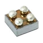
ICGOO电子元器件商城为您提供LD39130SJ29R由STMicroelectronics设计生产,在icgoo商城现货销售,并且可以通过原厂、代理商等渠道进行代购。 LD39130SJ29R价格参考¥5.14-¥10.45。STMicroelectronicsLD39130SJ29R封装/规格:PMIC - 稳压器 - 线性, Linear Voltage Regulator IC Positive Fixed 1 Output 2.9V 300mA 4-FlipChip (.69x.69)。您可以下载LD39130SJ29R参考资料、Datasheet数据手册功能说明书,资料中有LD39130SJ29R 详细功能的应用电路图电压和使用方法及教程。
STMicroelectronics(意法半导体)的LD39130SJ29R是一款PMIC(电源管理集成电路),属于线性稳压器类别。该型号的主要应用场景包括以下几方面:

 1. 便携式电子设备
   - LD39130SJ29R具有低功耗和高效率的特点,非常适合用于电池供电的便携式设备,如智能手机、平板电脑、可穿戴设备(智能手表、健康监测器等)。其稳定的电压输出可以为这些设备中的处理器、传感器和其他低功耗组件提供可靠的电源支持。

 2. 消费类电子产品
   - 在家用音频设备、游戏机控制器、遥控器等消费类电子产品中,这款线性稳压器能够提供稳定的电源供应,确保设备在各种工作条件下的性能一致性。

 3. 工业控制与自动化
   - 在工业领域,LD39130SJ29R可用于传感器接口、数据采集系统、PLC(可编程逻辑控制器)模块等场景。其出色的热管理和稳定性使其能够在恶劣的工业环境中可靠运行。

 4. 通信设备
   - 对于小型通信模块(如Wi-Fi模块、蓝牙模块或Zigbee模块),LD39130SJ29R可以为其提供精确的电压调节,确保信号传输的稳定性和可靠性。

 5. 医疗设备
   - 在便携式医疗设备(如血糖仪、脉搏血氧仪等)中,该稳压器的低噪声和高精度特性有助于提高测量的准确性,同时延长电池寿命。

 6. 物联网(IoT)设备
   - LD39130SJ29R适用于各种IoT节点和传感器设备,例如智能家居设备、环境监测器等。其高效的电源管理能力有助于降低功耗,延长设备的工作时间。

 核心优势:
- 低功耗:适合电池供电的应用。
- 高精度输出:确保设备运行的稳定性。
- 小封装尺寸:便于集成到紧凑型设计中。
- 良好的热性能:支持长时间稳定运行。

综上所述,LD39130SJ29R广泛应用于需要高效、稳定和低功耗电源管理的各种电子设备中。
| 参数 | 数值 |
| 产品目录 | 集成电路 (IC)半导体 |
| 描述 | IC REG LDO 2.9V 0.3A FLIPCHIP低压差稳压器 300mA current Linear Reg IC |
| 产品分类 | |
| 品牌 | STMicroelectronics |
| 产品手册 | |
| 产品图片 |
|
| rohs | 符合RoHS无铅 / 符合限制有害物质指令(RoHS)规范要求 |
| 产品系列 | 电源管理 IC,低压差稳压器,STMicroelectronics LD39130SJ29R- |
| mouser_ship_limit | 该产品可能需要其他文件才能进口到中国。 |
| 数据手册 | |
| 产品型号 | LD39130SJ29R |
| PSRR/纹波抑制—典型值 | 70 dB |
| 产品 | LDO Regulators |
| 产品培训模块 | http://www.digikey.cn/PTM/IndividualPTM.page?site=cn&lang=zhs&ptm=30339 |
| 产品种类 | 低压差稳压器 |
| 供应商器件封装 | 4-覆晶式 (.69x.69) |
| 其它名称 | 497-14208-6 |
| 包装 | Digi-Reel® |
| 商标 | STMicroelectronics |
| 回动电压—最大值 | 300 mV |
| 安装类型 | 表面贴装 |
| 安装风格 | SMD/SMT |
| 封装 | Reel |
| 封装/外壳 | 4-UFBGA,FCBGA |
| 封装/箱体 | FlipChip 4 |
| 工作温度 | -40°C ~ 125°C |
| 工厂包装数量 | 5000 |
| 最大功率耗散 | Internally Limited |
| 最大工作温度 | + 125 C |
| 最大输入电压 | 5.5 V |
| 最小工作温度 | + 40 C |
| 最小输入电压 | 1.4 V |
| 标准包装 | 1 |
| 电压-跌落(典型值) | 0.3V @ 300mA |
| 电压-输入 | 最高 5.5V |
| 电压-输出 | 2.9V |
| 电压调节准确度 | 1 % |
| 电流-输出 | 300mA |
| 电流-限制(最小值) | - |
| 电源电流 | 55 uA |
| 稳压器拓扑 | 正,固定式 |
| 稳压器数 | 1 |
| 类型 | Low Quiescent Current |
| 系列 | LD39130S |
| 线路调整率 | 0.02 % / V |
| 负载调节 | 1.5 % |
| 输出电压 | 2.9 V |
| 输出电压容差 | 1 % |
| 输出电流 | 300 mA |
| 输出端数量 | 1 Output |
| 输出类型 | Fixed |


- 商务部:美国ITC正式对集成电路等产品启动337调查
- 曝三星4nm工艺存在良率问题 高通将骁龙8 Gen1或转产台积电
- 太阳诱电将投资9.5亿元在常州建新厂生产MLCC 预计2023年完工
- 英特尔发布欧洲新工厂建设计划 深化IDM 2.0 战略
- 台积电先进制程称霸业界 有大客户加持明年业绩稳了
- 达到5530亿美元!SIA预计今年全球半导体销售额将创下新高
- 英特尔拟将自动驾驶子公司Mobileye上市 估值或超500亿美元
- 三星加码芯片和SET,合并消费电子和移动部门,撤换高东真等 CEO
- 三星电子宣布重大人事变动 还合并消费电子和移动部门
- 海关总署:前11个月进口集成电路产品价值2.52万亿元 增长14.8%


PDF Datasheet 数据手册内容提取
LD39130S Datasheet 300 mA very low quiescent current linear regulator IC with automatic green mode Features • Input voltage from 1.4 to 5.5 V • Ultra low dropout voltage (300 mV typ. at 300 mA load) • Automatic green mode • Very low quiescent current (1 µA in green mode, 45 µA in normal mode and 0.1 µA typ. in off mode) • Output voltage tolerance: ±1.0% at 25 °C • 300 mA guaranteed output current • Wide range of output voltages available on request: adjustable from 0.8 V, fixed up to 4.0 V in 100 mV step • Logic-controlled electronic shutdown • Internal soft-start • Compatible with ceramic capacitor C = 330 nF OUT • Internal current foldback and thermal protections • Available in DFN6 1.2x1.3 mm and Flip-chip 4 bumps 0.69 x 0.69 mm. 0.4 pitch • Operating temperature range: -40 °C to 125 °C Applications • Mobile phones • Digital still cameras (DSC) • Cordless phones and similar battery-powered systems Maturity status link • Portable media players LD39130S Description The LD39130S is a high accuracy voltage regulator that provides 300 mA maximum current from an input voltage ranging from 1.4 V to 5.5 V, with a typical dropout voltage of 300 mV. It is available in DFN6 1.2 x 1.3 mm package and in ultra-small CSP 4 bumps package, allowing the maximum space saving. The device is stabilized with a ceramic capacitor on the output. The ultra-low drop voltage, low quiescent current and low noise features make it suitable for low power battery-operated applications. It integrates an internal logic circuitry, which allows the regulator to be in ultra-low consumption mode (green mode), when the output current required is very low. The normal working mode, with fast transient response, is restored when the load current increases. The enable logic control function puts the LD39130S in shutdown mode allowing a total current consumption lower than 0.1 µA. The current foldback and thermal protection are provided. DS9919 - Rev 5 - July 2018 www.st.com For further information contact your local STMicroelectronics sales office.
LD39130S Block diagrams 1 Block diagrams Figure 2. Block diagram (adjustable version) VIN VIN Thermal protection Fast Bandgap turn-on & Short RC filter OPAMP circuit protection V OUT I OUT detection & Control Green Mode logic function GND EN GM ADJ Figure 3. Block diagram (fixed version) VIN VIN Thermal protection Fast Bandgap turn-on & Short RC filter OPAMP circuit protection V OUT I OUT detection & Control Green Mode logic function GND EN GM DS9919 - Rev 5 page 2/31
LD39130S Pin configuration 2 Pin configuration Figure 4. Pin connection (top view) 1 6 A2 B2 2 5 A1 B1 3 4 DFN6 Flip chip 4 Table 1. Pin description Pin n° Symbol Function DFN6 Flip chip Auto green mode selection: low = active, high = disabled. 1 GM This pin is internally pulled-down to GND. 2 B2 GND Common ground Enable pin logic input: low = shutdown, high = active. 3 B1 EN This pin is internally pulled-down to GND. 4 A1 IN Input voltage 5 ADJ/NC (1) Adjust pin 6 A2 OUT Output voltage 1. Not connected in the fixed output voltage version. DS9919 - Rev 5 page 3/31
LD39130S Typical applications 3 Typical applications Figure 5. Typical application circuits Adjustable version Fixed version VI VI VO VO VI VI VO VO ON ON OFF EN LD39130S R1 OFF EN LD39130S CIn GM GND ADJ COut CIn GM GND COut R 2 V =V (1+R1/R2) O ADJ Note: GM and ADJ pins are available on the DFN6 package only. DS9919 - Rev 5 page 4/31
LD39130S Maximum ratings 4 Maximum ratings Table 2. Absolute maximum ratings Symbol Parameter Value Unit VIN DC input voltage -0.3 to 7 V VOUT DC output voltage -0.3 to VI +0.3 V VEN Enable input voltage -0.3 to VI +0.3 V VGM Auto green mode input voltage -0.3 to VI +0.3 V VADJ Adjust pin voltage -0.3 to 2 V IOUT Output current Internally limited mA PD Power dissipation Internally limited mW TSTG Storage temperature range -65 to 150 °C TOP Operating junction temperature range -40 to 125 °C Note: Absolute maximum ratings are those values beyond which damage to the device may occur. Functional operation under these conditions is not implied. All values are referred to GND. Table 3. Thermal data Value Symbol Parameter Unit DFN6 Flip chip 4 RthJA Thermal resistance junction-ambient 237 130 °C/W RthJC Thermal resistance junction-case 104 °C/W Table 4. ESD performance Symbol Parameter Test conditions Value Unit HBM 2 kV ESD ESD protection voltage CDM(DFN version) 200 V CDM(CSP version) 300 V DS9919 - Rev 5 page 5/31
LD39130S Electrical characteristics 5 Electrical characteristics T = 25 °C, V = V + 1 V, C = C = 1 µF, I = 1 mA, V = V , unless otherwise specified. J IN OUT(NOM) IN OUT OUT EN IN Table 5. LD39130S/LD39130SJ electrical characteristics (fixed versions) Symbol Parameter Test conditions Min. Typ. Max. Unit VIN Operating input voltage 1.4 5.5 V VOUT > 2 V, IOUT = 10 mA, TJ = 25 °C -1.0 1.0 % VOUT accuracy VOUT > 2 V, IOUT = 10 mA, -40 °C < TJ < 125 °C -2 2 % (normal mode) VOUT ≤ 2 V, IOUT = 10 mA, TJ = 25 °C -20 20 mV VOUT ≤ 2 V, IOUT = 10 mA, -40 °C < TJ < 125 °C -30 30 mV VOUT VOUT > 2 V, IOUT = 1 mA, TJ = 25 °C -1.0 1.0 % VOUT accuracy VOUT > 2 V, IOUT = 1 mA,-40 °C < TJ < 125 °C -2 2 % (green mode) VOUT ≤ 2 V, IOUT = 1 mA, TJ = 25 °C -20 20 mV VOUT ≤ 2 V, IOUT = 1 mA, -40 °C < TJ < 125 °C -30 30 mV Static line regulation VOUT + 0.5V ≤ VIN ≤ 5.5 V, IOUT = 10 mA 0.02 0.20 %/V (normal mode) VIN > 1.4 V ΔVOUT Static line regulation VOUT + 0.5 V ≤ VIN ≤ 5.5 V, IOUT = 1 mA 0.50 %/V (green mode) VIN > 1.4 V VOUT > 2 V, IOUT = 1 mA to 12 mA -1.5 1.5 % ΔVOUT Static load regulation 12 mA to 300 mA (normal mode) 0.004 %/mA VDROP Dropout voltage (1) IOUT = 300 mA, VOUT > 2 V, -40 °C < TJ < 125 °C 300 mV eN Output noise voltage 1100 HHzz ttoo 110000 kkHHzz,, IIOOUUTT == 115 m mAA 13080 µVVORUMTS/ VIN = VOUTNOM + 1 V ±VRIPPLE, VRIPPLE = 0.1 V, 70 Supply voltage rejection freq. = 1 kHz, IOUT = 30 mA SVR VOUT = 1.5 V dB VIN = VOUTNOM + 0.5 V ±VRIPPLE, (normal mode) 65 VRIPPLE = 0.1 V, freq. = 10 kHz, IOUT = 30 mA Quiescent current (normal mode) IOUT = 10 mA 45 µA IQ Quiescent current (Green mode) IOUT = 0 mA 1 4 µA IStandby Standby current VIN input current in off mode: VEN = GND 0.1 1 µA ISC Short-circuit current RL = 0 (current foldback protection) 50 mA IOUT Output current 300 mA Enable input logic low VIN = 1.4 V to 5.5 V, -40 °C < TJ <1 25 °C 0.4 VEN V Enable input logic high VIN = 1.4 V to 5.5 V, -40 °C < TJ < 125 °C 1 IEN Enable pin input current VSHDN = VIN 100 nA Change from light load to normal load Normal mode switch IGH threshold VGM = GND (2) 10 mA DS9919 - Rev 5 page 6/31
LD39130S Electrical characteristics Symbol Parameter Test conditions Min. Typ. Max. Unit Change from normal load to light load Green mode switch IGL threshold VGM = GND 1 2 mA (2) VGM Green mode input logic low VIN = 1.4 V to 5.5 V, -40 °C < TJ < 125 °C 0.4 V (2) Green mode input logic high VIN = 1.4 V to 5.5 V, -40 °C < TJ < 125 °C 1 IGM Green mode pin current 100 nA (2) TON (3) Turn-on time 100 µs Output voltage discharge RON path resistance VEN = GND 100 Ω Thermal shutdown 160 TSHDN °C Hysteresis 20 Capacitance (see Section 7 Typical COUT Output capacitor characteristics) 0.33 22 µF 1. Dropout voltage is the input-to-output voltage difference at which the output voltage is 100 mV below its nominal value. 2. On DFN6 package version only. 3. Turn-on time is time measured between the enable input just exceeding VEN high value and the output voltage just reaching 95% of its nominal value. T = 25 °C, V = V + 1 V, C = C = 1 µF, I = 1 mA, V = V , unless otherwise specified. J IN OUT(NOM) IN OUT OUT EN IN Table 6. LD39130S electrical characteristics (adjustable version) Symbol Parameter Test conditions Min. Typ. Max. Unit VIN Operating input voltage 1.4 5.5 V VADJ accuracy IOUT = 5 mA, TJ = 25 °C 780 800 820 mV VADJ (fixed normal mode) IOUT = 5 mA, VGM = VIN, -40 °C < TJ < 125 °C 770 800 830 mV Static line regulation VOUT + 0.5 V ≤ VIN ≤ 5.5 V, IOUT = 10 mA, 0.02 0.20 %/V (normal mode) VIN > 1.4 V ΔVOUT Static line regulation VOUT + 0.5V ≤ VIN ≤ 5.5 V, IOUT = 1 mA, 0.20 %/V (green mode) VIN > 1.4 V VOUT > 2 V, IOUT = 1 mA to 12 mA -1.5 1.5 % ΔVOUT Static load regulation 10 mA to 300 mA (normal mode) 0.004 %/mA VDROP Dropout voltage (1) IOUT = 300 mA, VOUT > 2 V, -40 °C < TJ < 125 °C 300 mV 10 Hz to 100 kHz, IOUT = 1 mA, VOUT = VADJ 97 eN Output noise voltage µVRMS 10 Hz to 100 kHz, IOUT = 15 mA, VOUT = VADJ 41 VIN = VOUTNOM + 1 V ± VRIPPLE, VRIPPLE = 0.1 V, 70 freq. = 1 kHz, IOUT = 30 mA Supply voltage rejection SVR dB VOUT = 1.5V (normal mode) VIN = VOUTNOM + 0.5 V ± VRIPPLE, 65 VRIPPLE = 0.1 V, Freq. = 10 kHz, IOUT = 30 mA Quiescent current (normal mode) IOUT = 10 mA 45 µA IQ Quiescent current (Green mode) IOUT = 0 mA 0.8 4 µA IStandby Standby current VIN input current in OFF MODE: VEN = GND 0.1 1 µA DS9919 - Rev 5 page 7/31
LD39130S Electrical characteristics Symbol Parameter Test conditions Min. Typ. Max. Unit ISC Short-circuit current RL = 0 (current foldback protection) 50 mA IOUT Output current 300 mA Enable input logic low VIN = 1.4 V to 5.5 V, -40 °C < TJ < 125 °C 0.4 VEN V Enable input logic high VIN = 1.4 V to 5.5 V, -40 °C < TJ < 125 °C 1 IEN Enable pin input current VSHDN = VIN 100 nA Change from light load to normal load IGH Normal mode switch threshold VGM = GND 10 mA Change from normal load to light load IGL Green mode switch threshold 1 2 mA VGM = GND Green mode input logic low VIN = 1.4 V to 5.5 V, -40 °C < TJ < 125 °C 0.4 VGM V Green mode input logic high VIN = 1.4 V to 5.5 V, -40 °C < TJ < 125 °C 1 IGM Green mode pin current 100 nA TON (2) Turn on time 100 µs Output voltage discharge path RON resistance VEN = GND 100 Ω Thermal shutdown 160 TSHDN °C Hysteresis 20 Capacitance (see Section 7 Typical COUT Output capacitor characteristics) 0.33 22 µF 1. Dropout voltage is the input-to-output voltage difference at which the output voltage is 100 mV below its nominal value. 2. Turn-on time is time measured between the enable input just exceeding VEN high value and the output voltage just reaching 95% of its nominal value DS9919 - Rev 5 page 8/31
LD39130S Application information 6 Application information 6.1 Output voltage setting for ADJ version In the adjustable version, the output voltage can be set from 0.8 V to the input voltage minus the voltage drop across the pass transistor (dropout voltage), by connecting a resistor divider between the ADJ pin and the output, allowing remote voltage sensing. The resistor divider can be determined using the following equation: Equation 2 (1) R1 Even if the regulator is stable witVhO nUoT l=oaVdA,D tJh×e m1a+xiRm2um w ivtℎa lVuAeD fJo=r R02.8 Vshtoyupl.d not exceed 2 MΩ in order to ensure the best dynamic performance. 6.2 Soft-start function The LD39130S has an internal soft-start circuit. By increasing the startup time up to 100 µs, without the need of any external soft-start capacitor, this feature keeps the regulator inrush current at startup under control. 6.3 Auto green mode function The LD39130S integrates an internal logic circuitry, which allows the regulator to be in ultra-low consumption mode (green mode), when the output current required is very low. When the auto green mode is enabled, the regulator automatically selects its operating mode, switching from a very low consumption operation at light loads, to a very fast transient response mode when the load current increases. In the LD39130S, in DFN6 package, this function can be disabled by the user, by means of an external logic pin (GM). When the GM pin is set at high logic level, the device always operates in normal mode (fast transient response), while if the GM pin is set low, the auto green mode is enabled. The LD39130SJ (CSP version) always operates in auto green mode. 6.4 Input and output capacitors The LD39130S requires external capacitors to ensure the regulator control loop stability. These capacitors must be selected to meet the requirements of minimum capacitance and equivalent series resistance (see Figure 33. Stability plan vs. (COUT, ESR) ). Locating the input/output capacitors as close as possible to the relative pins, is suggested. 6.4.1 Input capacitor A capacitor with a minimum value of 1 µF is required at the input voltage of the LD39130S. This capacitor must be located as close as possible to the input pin of the device and returned to a clean analog ground. Any good quality ceramic capacitor can be used. 6.4.2 Output capacitor The control loop of the LD39130S is designed to work with ceramic capacitors at the output. The output capacitor must meet the requirements for the minimum amount of capacitance and E.S.R. (equivalent series resistance) as shown in Figure 33. Stability plan vs. (COUT, ESR) . The suggested value of 1 µF is a good choice to guarantee the stability of the regulator and to provide the optimum transient response. The output capacitor must maintain its ESR and capacitance in the stable region, over the full operating temperature range, to assure stability. DS9919 - Rev 5 page 9/31
LD39130S Output discharge function 6.5 Output discharge function The LD39130S integrates a MOSFET connected between V and GND. This transistor is activated when the OUT EN pin goes to low logic level and has the function to quickly discharge the output capacitor when the device is disabled by the user. DS9919 - Rev 5 page 10/31
LD39130S Typical characteristics 7 Typical characteristics (C = C = 1 µF, V = V = 1.8 V, V = V , T = 25 °C unless otherwise specified) IN OUT EN IN OUT ADJ j Figure 6. Output voltage vs. temperature Figure 7. Output voltage vs. temperature (VIN = 1.8 V, IOUT = 5 mA, normal mode) (VIN = 1.8 V, IOUT = 300 mA, normal mode) VIN= 1.8 V, IOUT = 5 mA, VEN = 1.8 V, VGM = 1 V (normal mode) VIN= 1.8 V, IOUT = 300 mA, VEN = 1.8 V, VGM = 1 V (normal mode) 850 850 840 840 830 830 Voltage[mV] 888012000 Voltage[mV] 888012000 Output 778900 Output 778900 770 770 760 760 750 750 -40 -25 0 25 55 85 125 -40 -25 0 25 55 85 125 Temperature[°C] Temperature[°C] Figure 8. Output voltage vs. temperature Figure 9. Output voltage vs. temperature (V = 1.4 V, I = 1 mA, auto green mode) (V = 5.5 V, I = 1 mA, auto green mode) IN OUT IN OUT VIN= 1.4 V, IOUT = 1 mA, VEN = 1.4 V, VGM = 0.4 V (auto green mode) VIN= 5.5 V, IOUT = 1 mA, VEN = 5.5 V, VGM = 0.4 V (auto green mode) 850 850 840 840 830 830 820 820 OutputVoltage[mV] 778889010000 OutputVoltage[mV] 778889010000 770 770 760 760 750 750 -40 -25 0 25 55 85 125 -40 -25 0 25 55 85 125 Temperature[°C] Temperature[°C] Figure 10. Line regulation vs. temperature (normal Figure 11. Line regulation vs. temperature (auto mode) green mode) 0.2 VIN=1.4 to 5.5 V, IOUT = 10 mA, VEN = VIN, VGM = 1 V (normal mode) 0.2 VIN=1.4 to 5.5 V, IOUT = 1 mA, VEN = VIN, VGM = 0.4 V (auto green mode) 0.18 0.18 0.16 0.16 %/V]0.14 %/V]0.14 Lineregulation[000...0001.6821 Lineregulation[000...0001.6821 0.04 0.04 0.02 0.02 0 -40 -25 0 25 55 85 125 0 -40 -25 0 25 55 85 125 Temperature[°C] Temperature[°C] DS9919 - Rev 5 page 11/31
LD39130S Typical characteristics Figure 12. Load regulation vs. temperature (IOUT = 1 Figure 13. Load regulation vs. temperature to 10 mA, normal mode) (I = 10 to 300 mA, normal mode) OUT 0.003 VIN=1.8 V, IOUT = 1 to 10 mA, VEN = VIN, VGM = 1 V (normal mode) 0.005 VIN=1.8 V, IOUT = 10 to 300 mA, VEN = VIN, VGM = 1 V (normal mode) 0.0045 0.0025 0.004 Loadregulation[%/mA]0.000..000100512 Loadregulation[%/mA]000...00000..000001230055523 0.001 0.0005 0.0005 0 0 -40 -25 0 25 55 85 125 -40 -25 0 25 55 85 125 Temperature[°C] Temperature[°C] Figure 15. Mode change thresholds vs. Figure 14. Load regulation vs. temperature (I = 1 OUT temperature to 12 mA, auto green mode) 0.5VIN=1.8 V, IOUT = 1 to 12 mA, VEN = VIN, VGM = 0.4 V (auto green mode) 7 VIN=1.8 V, IOUT = 1 mA, VEN = VIN, VGM = 0 V (auto grGereenen m too Ndoerm)al Normal to Green 0.45 6 A] 0.4 m regulation[%/mA] 00..0023..5523 angethresholds[345 Load 0.01.51 Modech2 1 0.05 0 -40 -25 0 25 55 85 125 0 -40 -25 0 25 55 85 125 Temperature[°C] Temperature[°C] Figure 16. Quiescent current vs. temperature Figure 17. Quiescent current vs. temperature (IOUT = 10 mA, normal mode) (IOUT = 300 mA, normal mode) 80 VIN=1.8 V, IOUT = 10 mA, VEN = VIN, VGM = 1 V VIN=1.8 V, IOUT = 300 mA, VEN = VIN, VGM = 1 V 140 70 120 60 current[µA] 4500 current[µA] 10800 Quiescent 2300 Quiescent 4600 10 20 0 0 -40 -25 0 25 55 85 125 -40 -25 0 25 55 85 125 Temperature[°C] Temperature[°C] DS9919 - Rev 5 page 12/31
LD39130S Typical characteristics Figure 18. Quiescent current vs. temperature (no Figure 19. Shutdown current vs. temperature load, auto green mode) 5 VIN=1.8 V, IOUT = 0 mA, VEN = VIN, VGM = 0.4 V 3 VIN=1.8 V, IOUT = 0 mA, VEN = VIN, VGM = GND 4.5 2.5 4 Quiescentcurrent[µA] 123...55523 Quiescentcurrent[µA] 1.512 1 0.5 0.5 0 0 -40 -25 0 25 55 85 125 -40 -25 0 25 55 85 125 Temperature[°C] Temperature[°C] Figure 20. Quiescent current vs. input voltage (auto Figure 21. Quiescent current vs. input voltage green mode) (normal mode) IOUT=0mA IOUT = 0 mA 4 3 3.5 2.5 Quiescentcurrent[µA] 12..5523 Quiescentcurrent[µA] 1.512 1 0.5 0.5 0 0 0 1 2 3 4 5 6 0 1 2 3 4 5 6 InputVoltage[V] InputVoltage[V] Figure 22. Quiescent current vs. output current Figure 23. Quiescent current vs. load current (auto green mode) (normal mode) 90 100 80 90 70 80 A] Quiescent current [µ 34560000 VVVVIIIINNNN====1513....8540VVVV Quiescentcurrent[µA] 3456700000 20 20 10 10 0 0 0 50 100 150 200 250 300 350 1 10 100 LoadCurrent[mA] Load current [mA] DS9919 - Rev 5 page 13/31
LD39130S Typical characteristics Figure 24. Quiescent current vs. load current (light Figure 25. Short-circuit current vs. output voltage load) IOUT = 0 mA VIN=2V, VOUT=VADJ ,T=25°C 600 25 500 20 A] Green Mode High m 400 Quiescent current [µA] 1105 Green Mode Low Shortcircuitcurrent[ 230000 5 100 0 0 0 100 200 300 400 500 600 700 800 0 0.5 1 1.5 2 2.5 3 Load current [mA] OutputVoltage[mV] Figure 26. Foldback current vs. temperature Figure 27. Dropout voltage vs. temperature 60 VIN=1.8 V, VOUT = GND, VEN = VIN, VGM = 1 V 200 VOUT= 4.1 V 58 180 56 160 A] [m 54 mV] 140 current 5502 Voltage[ 110200 IIoouutt==310000mmAA Foldback 4468 Dropout 6800 44 40 42 20 40 0 -40 -25 0 25 55 85 125 -40 -25 0 25 55 85 125 Temperature[°C] Temperature[°C] Figure 28. Dropout voltage vs. output current Figure 29. SVR vs. frequency (normal mode) 160 VOUT= 4.1 V 90 VIN=1.8 +/- 200 m V, IOUT = 10 mA, VOUT = 0.8 V, CIN = COUT = 1 µF (normal mode) 140 80 120 70 DropoutVoltage[mV] 1068000 SVR[dB] 34560000 40 20 20 10 0 1 5 10 50 100 200 300 0100 1000 10000 100000 1000000 Output current[mA] Frequency[Hz] DS9919 - Rev 5 page 14/31
LD39130S Typical characteristics Figure 31. Noise spectrum vs. frequency Figure 30. SVR vs. frequency (green mode) (V = V ) OUT ADJ 90 VIN=1.8 +/- 200 m V, IOUT = 3 mA, VOUT = 0.8 V, CIN = COUT = 1 µF (green mode) VOUT = VADJ 7.0 80 70 6.0 ILOAD=0A [dB] 60 5.0 IILLOOAADD==13m0mAA SVR 50 RT(Hz)] 4.0 3400 N[uV/ SQ 3.0 20 e 2.0 10 1.0 0 100 1000 10000 100000 1000000 0.0 Frequency[Hz] 1.E+01 1.E+02 1.E+03 1.E+04 1.E+05 Frequency[Hz] Figure 32. Noise spectrum vs. frequency Figure 33. Stability plan vs. (COUT, ESR) (V = 4.1 V) OUT 4 VOUT = 4.1 V 25.0 3.5 3 20.0 IILLOOAADD ==01AmA Hz[Ω]2.5 QRT(Hz)]15.0 ILOAD =30mA @100K 2 STABILITYAREA N[uV/ S10.0 ESR1.51 e 5.0 0.5 0 0 1 2 3 4 5 6 7 8 9 1011121314151617181920212223 0.0 1.E+01 1.E+02 1.E+03 1.E+04 1.E+05 COUT[µF] (nominal value) Frequency[Hz] Figure 34. Startup by enable (I = 0 mA, auto Figure 35. Turn-off by enable (I = 0 mA, auto OUT OUT green mode) green mode) VIN=1.5 V, VEN = 0 V to VIN, IOUT = 0 mA, VOUT = 0.8 V, Tr = 1 µs (auto green mode) VIN=1.5 V, VEN = VIN to 0 V, IOUT = 0 mA, VOUT = 0.8 V, Tf = 1 µs (auto green mode) VOUT VOUT VEN VEN DS9919 - Rev 5 page 15/31
LD39130S Typical characteristics Figure 37. Turn-off by enable Figure 36. Startup by enable VIN = 1.5V, VEN = VIN to 0 V, IOUT = 300 mA, VOUT = 0.8 V, Tf= 1 µs, (auto green mode) VIN=1.5 V, VEN = 0Vto VIN, IOUT = 300 mA, VOUT = 0.8 V, Tr = 1 µs (auto green mode) I OUT I OUT V OUT V OUT V EN V EN Figure 38. Startup by enable (IOUT = 300 mA, Figure 39. Turn-off by enable (IOUT = 300 mA, normal mode) normal mode) VIN=1.5 V, VEN = 0 Vto VIN,VGM = VIN, IOUT = 300 mA, VOUT = 0.8 V, Tf = 1 µs (fixed normal mode) VIN=1.5 V, VEN = VIN to 0 V,VGM = VIN, IOUT = 300 mA, VOUT = 0.8 V, Tf = 1 µs (fixed normal mode) IOUT IOUT VOUT VOUT VEN VEN Figure 40. Turn-on time Figure 41. Turn-off time VIN= VEN = 0 V to 5.5 V, IOUT = 300 mA, VOUT = 0.8 V, Tf = 5 µs VIN= VEN = 5.5 V to 0 V , IOUT = 300 mA, VOUT = 0.8 V, Tf = 5 µs I OUT IOUT V OUT VOUT V V EN, IN VEN,VIN DS9919 - Rev 5 page 16/31
LD39130S Typical characteristics Figure 42. Line transient (auto green mode) Figure 43. Line transient (normal mode) VIN= VEN = 1.8 V to 2.3 V , IOUT = 1 mA, VOUT = 0.8 V, Tf = 5 µs (green mode) VIN= VEN = 1.8 V to 2.3 V , IOUT = 12 mA, VOUT = 0.8 V, Tf = 5 µs (normal mode) VOUT VOUT VEN,VIN VEN,VIN Figure 44. Load transient (I = 1 to 30 mA, auto Figure 45. Load transient (I = 0 to 300 mA, auto OUT OUT green mode) green mode) IOUT = from 1 to 30 mA, VOUT = 0.8 V, Tr = Tf = 0.5 µs (auto green mode) IOUT = from 0 to 300 mA, VOUT = 0.8 V, Tr = Tf = 0.5 µs (auto green mode) VOUT VOUT IOUT IOUT Figure 46. Load transient (IOUT = 1 to 300 mA, Figure 47. Green mode transient normal mode) IOUT = 0 mA, VOUT = 0.8 V, Tr = Tf = 1 µs, VGM = from 0 V to Vin IOUT = from 1 to 300 mA, VOUT = 0.8 V, Tr = Tf = 5 µs, VGM = Vin (normal mode) VOUT VOUT VGM IOUT DS9919 - Rev 5 page 17/31
LD39130S Package information 8 Package information In order to meet environmental requirements, ST offers these devices in different grades of ECOPACK® packages, depending on their level of environmental compliance. ECOPACK® specifications, grade definitions and product status are available at: www.st.com. ECOPACK® is an ST trademark. 8.1 Flip-chip 4 package information Figure 48. Flip-chip 4 package mechanical outline 8288567 rev 5 DS9919 - Rev 5 page 18/31
LD39130S Flip-chip 4 package information Table 7. Flip-chip 4 mechanical data mm Dim. Min. Typ. Max. A 0.445 0.48 0.515 A1 0.065 0.08 0.095 A2 0.38 0.40 0.42 b 0.12 0.16 0.2 D 0.66 0.69 0.72 D1 0.40 E 0.66 0.69 0.72 E1 0.40 f 0.135 0.145 0.155 SD/SE 0.20 ccc 0.02 Figure 49. Flip-chip 4 package footprint 8288567 rev 5 DS9919 - Rev 5 page 19/31
LD39130S DFN6 1.2x1.3 mm package information 8.2 DFN6 1.2x1.3 mm package information Figure 50. DFN6 1.2x1.3 mm package mechanical outline DS9919 - Rev 5 page 20/31
LD39130S DFN6 1.2x1.3 mm package information Table 8. DFN6 1.2x1.3 mm mechanical data mm Dim. Min. Typ. Max. A 0.31 0.38 0.40 A1 0.00 0.02 0.05 b 0.15 0.18 0.25 D 1.10 1.20 1.30 E 1.20 1.30 1.40 e 0.40 BSC L 0.475 0.525 0.575 L3 0.375 0.425 0.475 N 6 ND 3 Figure 51. DFN6 1.2x1.3 mm package footprint DS9919 - Rev 5 page 21/31
LD39130S Packing information 9 Packing information Figure 52. Flip-chip 4 tape DS9919 - Rev 5 page 22/31
LD39130S Packing information Figure 53. Flip-chip 4 reel oriented MARKING VIEW DOT Figure 54. DFN6 tape Figure 55. DFN6 reel oriented DS9919 - Rev 5 page 23/31
LD39130S Packing information Table 9. Reel mechanical data mm Dim. Min. Typ. Max. A 180 C 12.8 13 13.2 D 20.2 N 60 T 14.4 Figure 56. Reel outline N D C A T Note: Drawing not in scale DS9919 - Rev 5 page 24/31
LD39130S Order codes 10 Order codes Table 10. Order codes Order codes Output voltages (V) Marking digits (XY) DFN6 1.2x1.3 mm Flip-chip 4 LD39130SPUR Adjustable AD LD39130SJ10R 1.0 10 LD39130SJ12R 1.2 12 LD39130SJ18R 1.8 18 LD39130SPU25R LD39130SJ25R 2.5 25 LD39130SJ29R 2.9 29 LD39130SJ30R 3.0 30 LD39130SPU31R 3.1 31 LD39130SJ33R 3.3 33 LD39130SJ41R 4.1 41 Note: Other output voltage versions available on request. Figure 57. Flip-chip and DFN6 1.2x1.3 marking composition (marking view) 1 6 XY XY 2 5 3 4 Note: “xy” indicates the marking digits, as per Table 10. Order codes. DS9919 - Rev 5 page 25/31
LD39130S Revision history Table 11. Document revision history Date Revision Changes 08-Oct-2013 1 Initial release. Updated Figure 19: Quiescent current vs. input voltage (auto green mode) and Figure 23: Quiescent current vs. load current (light load) Updated Table 3: Thermal data, Table 4: ESD performance, Table 5: LD39130S/LD39130SJ electrical characteristics (fixed versions), Table 6: LD39130S electrical characteristics (adjustable 20-Jan-2015 2 version), Figure 19: Quiescent current vs. input voltage (auto green mode), Figure 23: Quiescent current vs. load current (light load), Figure 39: Turn-on time and Figure 41: Line transient (auto green mode). Minor text changes. Throughout document: - minor text and formatting changes In Table 1. Pin description: - updated GM and EN function descriptions 04-Apr-2018 3 Updated Figure 5. Typical application circuits Added Section 6.1 Output voltage setting for ADJ version Updated Section 7 Typical characteristics Updated Table 9. Order codes 13-Jun-2018 4 Updated Figure 50. DFN6 1.2x1.3 mm package mechanical outline. 06-Jul-2018 5 Updated Table 8. DFN6 1.2x1.3 mm mechanical data. DS9919 - Rev 5 page 26/31
LD39130S Contents Contents 1 Block diagrams....................................................................2 2 Pin configuration ..................................................................3 3 Typical applications ...............................................................4 4 Maximum ratings ..................................................................5 5 Electrical characteristics...........................................................6 6 Application information............................................................9 6.1 Output voltage setting for ADJ version.............................................9 6.2 Soft-start function ..............................................................9 6.3 Auto green mode function .......................................................9 6.4 Input and output capacitors ......................................................9 6.4.1 Input capacitor ..........................................................9 6.4.2 Output capacitor .........................................................9 6.5 Output discharge function .......................................................9 7 Typical characteristics............................................................11 8 Package information..............................................................18 8.1 Flip-chip 4 package information..................................................18 8.2 DFN6 1.2x1.3 mm package information...........................................19 9 Packing information ..............................................................22 10 Order codes ......................................................................25 Revision history .......................................................................26 Contents ..............................................................................27 List of tables ..........................................................................28 List of figures..........................................................................29 DS9919 - Rev 5 page 27/31
LD39130S List of tables List of tables Table 1. Pin description. . . . . . . . . . . . . . . . . . . . . . . . . . . . . . . . . . . . . . . . . . . . . . . . . . . . . . . . . . . . . . . . . . . . . . 3 Table 2. Absolute maximum ratings . . . . . . . . . . . . . . . . . . . . . . . . . . . . . . . . . . . . . . . . . . . . . . . . . . . . . . . . . . . . . 5 Table 3. Thermal data. . . . . . . . . . . . . . . . . . . . . . . . . . . . . . . . . . . . . . . . . . . . . . . . . . . . . . . . . . . . . . . . . . . . . . . 5 Table 4. ESD performance . . . . . . . . . . . . . . . . . . . . . . . . . . . . . . . . . . . . . . . . . . . . . . . . . . . . . . . . . . . . . . . . . . . 5 Table 5. LD39130S/LD39130SJ electrical characteristics (fixed versions) . . . . . . . . . . . . . . . . . . . . . . . . . . . . . . . . . . . 6 Table 6. LD39130S electrical characteristics (adjustable version). . . . . . . . . . . . . . . . . . . . . . . . . . . . . . . . . . . . . . . . . 7 Table 7. Flip-chip 4 mechanical data. . . . . . . . . . . . . . . . . . . . . . . . . . . . . . . . . . . . . . . . . . . . . . . . . . . . . . . . . . . . 19 Table 8. DFN6 1.2x1.3 mm mechanical data . . . . . . . . . . . . . . . . . . . . . . . . . . . . . . . . . . . . . . . . . . . . . . . . . . . . . . 21 Table 9. Reel mechanical data. . . . . . . . . . . . . . . . . . . . . . . . . . . . . . . . . . . . . . . . . . . . . . . . . . . . . . . . . . . . . . . . 24 Table 10. Order codes . . . . . . . . . . . . . . . . . . . . . . . . . . . . . . . . . . . . . . . . . . . . . . . . . . . . . . . . . . . . . . . . . . . . . . 25 Table 11. Document revision history. . . . . . . . . . . . . . . . . . . . . . . . . . . . . . . . . . . . . . . . . . . . . . . . . . . . . . . . . . . . . 26 DS9919 - Rev 5 page 28/31
LD39130S List of figures List of figures Figure 2. Block diagram (adjustable version) . . . . . . . . . . . . . . . . . . . . . . . . . . . . . . . . . . . . . . . . . . . . . . . . . . . . . . 2 Figure 3. Block diagram (fixed version) . . . . . . . . . . . . . . . . . . . . . . . . . . . . . . . . . . . . . . . . . . . . . . . . . . . . . . . . . . 2 Figure 4. Pin connection (top view). . . . . . . . . . . . . . . . . . . . . . . . . . . . . . . . . . . . . . . . . . . . . . . . . . . . . . . . . . . . . 3 Figure 5. Typical application circuits . . . . . . . . . . . . . . . . . . . . . . . . . . . . . . . . . . . . . . . . . . . . . . . . . . . . . . . . . . . . 4 Figure 6. Output voltage vs. temperature (V = 1.8 V, I = 5 mA, normal mode). . . . . . . . . . . . . . . . . . . . . . . . . . . 11 IN OUT Figure 7. Output voltage vs. temperature (V = 1.8 V, I = 300 mA, normal mode) . . . . . . . . . . . . . . . . . . . . . . . . . 11 IN OUT Figure 8. Output voltage vs. temperature (V = 1.4 V, I = 1 mA, auto green mode) . . . . . . . . . . . . . . . . . . . . . . . . 11 IN OUT Figure 9. Output voltage vs. temperature (V = 5.5 V, I = 1 mA, auto green mode) . . . . . . . . . . . . . . . . . . . . . . . . 11 IN OUT Figure 10. Line regulation vs. temperature (normal mode). . . . . . . . . . . . . . . . . . . . . . . . . . . . . . . . . . . . . . . . . . . . . 11 Figure 11. Line regulation vs. temperature (auto green mode) . . . . . . . . . . . . . . . . . . . . . . . . . . . . . . . . . . . . . . . . . . 11 Figure 12. Load regulation vs. temperature (I = 1 to 10 mA, normal mode). . . . . . . . . . . . . . . . . . . . . . . . . . . . . . . 12 OUT Figure 13. Load regulation vs. temperature (I = 10 to 300 mA, normal mode) . . . . . . . . . . . . . . . . . . . . . . . . . . . . . 12 OUT Figure 14. Load regulation vs. temperature (I = 1 to 12 mA, auto green mode) . . . . . . . . . . . . . . . . . . . . . . . . . . . . 12 OUT Figure 15. Mode change thresholds vs. temperature. . . . . . . . . . . . . . . . . . . . . . . . . . . . . . . . . . . . . . . . . . . . . . . . . 12 Figure 16. Quiescent current vs. temperature (I = 10 mA, normal mode) . . . . . . . . . . . . . . . . . . . . . . . . . . . . . . . . 12 OUT Figure 17. Quiescent current vs. temperature (I = 300 mA, normal mode) . . . . . . . . . . . . . . . . . . . . . . . . . . . . . . . 12 OUT Figure 18. Quiescent current vs. temperature (no load, auto green mode). . . . . . . . . . . . . . . . . . . . . . . . . . . . . . . . . . 13 Figure 19. Shutdown current vs. temperature . . . . . . . . . . . . . . . . . . . . . . . . . . . . . . . . . . . . . . . . . . . . . . . . . . . . . 13 Figure 20. Quiescent current vs. input voltage (auto green mode). . . . . . . . . . . . . . . . . . . . . . . . . . . . . . . . . . . . . . . . 13 Figure 21. Quiescent current vs. input voltage (normal mode) . . . . . . . . . . . . . . . . . . . . . . . . . . . . . . . . . . . . . . . . . . 13 Figure 22. Quiescent current vs. output current (auto green mode). . . . . . . . . . . . . . . . . . . . . . . . . . . . . . . . . . . . . . . 13 Figure 23. Quiescent current vs. load current (normal mode). . . . . . . . . . . . . . . . . . . . . . . . . . . . . . . . . . . . . . . . . . . 13 Figure 24. Quiescent current vs. load current (light load). . . . . . . . . . . . . . . . . . . . . . . . . . . . . . . . . . . . . . . . . . . . . . 14 Figure 25. Short-circuit current vs. output voltage . . . . . . . . . . . . . . . . . . . . . . . . . . . . . . . . . . . . . . . . . . . . . . . . . . 14 Figure 26. Foldback current vs. temperature . . . . . . . . . . . . . . . . . . . . . . . . . . . . . . . . . . . . . . . . . . . . . . . . . . . . . . 14 Figure 27. Dropout voltage vs. temperature. . . . . . . . . . . . . . . . . . . . . . . . . . . . . . . . . . . . . . . . . . . . . . . . . . . . . . . 14 Figure 28. Dropout voltage vs. output current. . . . . . . . . . . . . . . . . . . . . . . . . . . . . . . . . . . . . . . . . . . . . . . . . . . . . . 14 Figure 29. SVR vs. frequency (normal mode). . . . . . . . . . . . . . . . . . . . . . . . . . . . . . . . . . . . . . . . . . . . . . . . . . . . . . 14 Figure 30. SVR vs. frequency (green mode) . . . . . . . . . . . . . . . . . . . . . . . . . . . . . . . . . . . . . . . . . . . . . . . . . . . . . . 15 Figure 31. Noise spectrum vs. frequency (V = V ) . . . . . . . . . . . . . . . . . . . . . . . . . . . . . . . . . . . . . . . . . . . . . . 15 OUT ADJ Figure 32. Noise spectrum vs. frequency (V = 4.1 V). . . . . . . . . . . . . . . . . . . . . . . . . . . . . . . . . . . . . . . . . . . . . . 15 OUT Figure 33. Stability plan vs. (COUT, ESR) . . . . . . . . . . . . . . . . . . . . . . . . . . . . . . . . . . . . . . . . . . . . . . . . . . . . . . . . 15 Figure 34. Startup by enable (I = 0 mA, auto green mode) . . . . . . . . . . . . . . . . . . . . . . . . . . . . . . . . . . . . . . . . . . 15 OUT Figure 35. Turn-off by enable (I = 0 mA, auto green mode). . . . . . . . . . . . . . . . . . . . . . . . . . . . . . . . . . . . . . . . . . 15 OUT Figure 36. Startup by enable . . . . . . . . . . . . . . . . . . . . . . . . . . . . . . . . . . . . . . . . . . . . . . . . . . . . . . . . . . . . . . . . . 16 Figure 37. Turn-off by enable. . . . . . . . . . . . . . . . . . . . . . . . . . . . . . . . . . . . . . . . . . . . . . . . . . . . . . . . . . . . . . . . . 16 Figure 38. Startup by enable (I = 300 mA, normal mode). . . . . . . . . . . . . . . . . . . . . . . . . . . . . . . . . . . . . . . . . . . 16 OUT Figure 39. Turn-off by enable (I = 300 mA, normal mode). . . . . . . . . . . . . . . . . . . . . . . . . . . . . . . . . . . . . . . . . . . 16 OUT Figure 40. Turn-on time. . . . . . . . . . . . . . . . . . . . . . . . . . . . . . . . . . . . . . . . . . . . . . . . . . . . . . . . . . . . . . . . . . . . . 16 Figure 41. Turn-off time. . . . . . . . . . . . . . . . . . . . . . . . . . . . . . . . . . . . . . . . . . . . . . . . . . . . . . . . . . . . . . . . . . . . . 16 Figure 42. Line transient (auto green mode) . . . . . . . . . . . . . . . . . . . . . . . . . . . . . . . . . . . . . . . . . . . . . . . . . . . . . . 17 Figure 43. Line transient (normal mode) . . . . . . . . . . . . . . . . . . . . . . . . . . . . . . . . . . . . . . . . . . . . . . . . . . . . . . . . . 17 Figure 44. Load transient (I = 1 to 30 mA, auto green mode) . . . . . . . . . . . . . . . . . . . . . . . . . . . . . . . . . . . . . . . . 17 OUT Figure 45. Load transient (I = 0 to 300 mA, auto green mode). . . . . . . . . . . . . . . . . . . . . . . . . . . . . . . . . . . . . . . . 17 OUT Figure 46. Load transient (I = 1 to 300 mA, normal mode) . . . . . . . . . . . . . . . . . . . . . . . . . . . . . . . . . . . . . . . . . . 17 OUT Figure 47. Green mode transient . . . . . . . . . . . . . . . . . . . . . . . . . . . . . . . . . . . . . . . . . . . . . . . . . . . . . . . . . . . . . . 17 Figure 48. Flip-chip 4 package mechanical outline . . . . . . . . . . . . . . . . . . . . . . . . . . . . . . . . . . . . . . . . . . . . . . . . . . 18 Figure 49. Flip-chip 4 package footprint. . . . . . . . . . . . . . . . . . . . . . . . . . . . . . . . . . . . . . . . . . . . . . . . . . . . . . . . . . 19 Figure 50. DFN6 1.2x1.3 mm package mechanical outline. . . . . . . . . . . . . . . . . . . . . . . . . . . . . . . . . . . . . . . . . . . . . 20 Figure 51. DFN6 1.2x1.3 mm package footprint. . . . . . . . . . . . . . . . . . . . . . . . . . . . . . . . . . . . . . . . . . . . . . . . . . . . 21 DS9919 - Rev 5 page 29/31
LD39130S List of figures Figure 52. Flip-chip 4 tape. . . . . . . . . . . . . . . . . . . . . . . . . . . . . . . . . . . . . . . . . . . . . . . . . . . . . . . . . . . . . . . . . . . 22 Figure 53. Flip-chip 4 reel oriented. . . . . . . . . . . . . . . . . . . . . . . . . . . . . . . . . . . . . . . . . . . . . . . . . . . . . . . . . . . . . 23 Figure 54. DFN6 tape. . . . . . . . . . . . . . . . . . . . . . . . . . . . . . . . . . . . . . . . . . . . . . . . . . . . . . . . . . . . . . . . . . . . . . 23 Figure 55. DFN6 reel oriented . . . . . . . . . . . . . . . . . . . . . . . . . . . . . . . . . . . . . . . . . . . . . . . . . . . . . . . . . . . . . . . . 23 Figure 56. Reel outline . . . . . . . . . . . . . . . . . . . . . . . . . . . . . . . . . . . . . . . . . . . . . . . . . . . . . . . . . . . . . . . . . . . . . 24 Figure 57. Flip-chip and DFN6 1.2x1.3 marking composition (marking view) . . . . . . . . . . . . . . . . . . . . . . . . . . . . . . . . 25 DS9919 - Rev 5 page 30/31
LD39130S IMPORTANT NOTICE – PLEASE READ CAREFULLY STMicroelectronics NV and its subsidiaries (“ST”) reserve the right to make changes, corrections, enhancements, modifications, and improvements to ST products and/or to this document at any time without notice. Purchasers should obtain the latest relevant information on ST products before placing orders. ST products are sold pursuant to ST’s terms and conditions of sale in place at the time of order acknowledgement. Purchasers are solely responsible for the choice, selection, and use of ST products and ST assumes no liability for application assistance or the design of Purchasers’ products. No license, express or implied, to any intellectual property right is granted by ST herein. Resale of ST products with provisions different from the information set forth herein shall void any warranty granted by ST for such product. ST and the ST logo are trademarks of ST. All other product or service names are the property of their respective owners. Information in this document supersedes and replaces information previously supplied in any prior versions of this document. © 2018 STMicroelectronics – All rights reserved DS9919 - Rev 5 page 31/31
Mouser Electronics Authorized Distributor Click to View Pricing, Inventory, Delivery & Lifecycle Information: S TMicroelectronics: LD39130SJ33R LD39130SJ12R LD39130SJ29R LD39130SJ41R LD39130SJ10R LD39130SJ25R LD39130SJ18R LD39130SJ30R LD39130SPUR LD39130SPU25R LD39130SPU31R