ICGOO在线商城 > 集成电路(IC) > PMIC - 稳压器 - 线性 > NCP4587DMX28TCG
 Datasheet下载
- 型号: NCP4587DMX28TCG
- 制造商: ON Semiconductor
- 库位|库存: xxxx|xxxx
- 要求:
| 数量阶梯 | 香港交货 | 国内含税 |
| +xxxx | $xxxx | ¥xxxx |
查看当月历史价格
查看今年历史价格
NCP4587DMX28TCG产品简介:
ICGOO电子元器件商城为您提供NCP4587DMX28TCG由ON Semiconductor设计生产,在icgoo商城现货销售,并且可以通过原厂、代理商等渠道进行代购。 NCP4587DMX28TCG价格参考。ON SemiconductorNCP4587DMX28TCG封装/规格:PMIC - 稳压器 - 线性, Linear Voltage Regulator IC 1 Output 150mA 6-XDFN (1.2x1.2)。您可以下载NCP4587DMX28TCG参考资料、Datasheet数据手册功能说明书,资料中有NCP4587DMX28TCG 详细功能的应用电路图电压和使用方法及教程。
ON Semiconductor(安森美)的NCP4587DMX28TCG是一款低压差线性稳压器(LDO),属于PMIC - 稳压器 - 线性产品类别。该器件输出电压固定为2.8V,最大输出电流可达500mA,具有低静态电流、高电源抑制比(PSRR)和良好的负载/线路调节性能,适用于对噪声敏感和功耗要求严格的便携式设备。

典型应用场景包括:
1. 移动通信设备:如智能手机、平板电脑中的基带处理器、射频模块或传感器供电,因其低噪声特性可有效减少对信号链的干扰。
2. 便携式电子产品:用于蓝牙耳机、可穿戴设备(如智能手表、健康监测设备),得益于其小封装(如DFN)、低功耗和高效率,在电池供电系统中延长续航时间。
3. 消费类电子:适用于数码相机、MP3播放器等对空间和功耗敏感的产品。
4. 工业与物联网终端:为低功耗微控制器(MCU)、传感器节点、无线收发模块提供稳定电源,适合在宽温度范围内可靠运行。
5. 电源管理子系统:常作为多路电源方案中的辅助稳压单元,为噪声敏感的模拟电路(如ADC、音频放大器)提供干净电源。

NCP4587DMX28TCG集成过温保护和过流保护功能,提升了系统可靠性,同时支持陶瓷电容,减小外围元件体积,适合高密度PCB设计。综合来看,该LDO广泛应用于需高效、稳定、低噪声直流电源的中低端功率场景。
| 参数 | 数值 |
| 产品目录 | 集成电路 (IC)半导体 |
| 描述 | IC REG LDO 2.8V 0.15A 6XDFN低压差稳压器 3-MODE 150 MA LDO REG |
| 产品分类 | |
| 品牌 | ON Semiconductor |
| 产品手册 | |
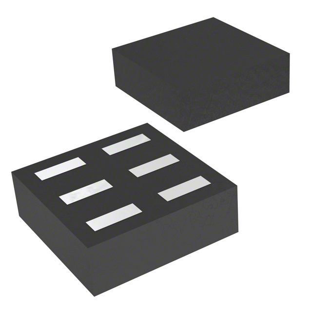
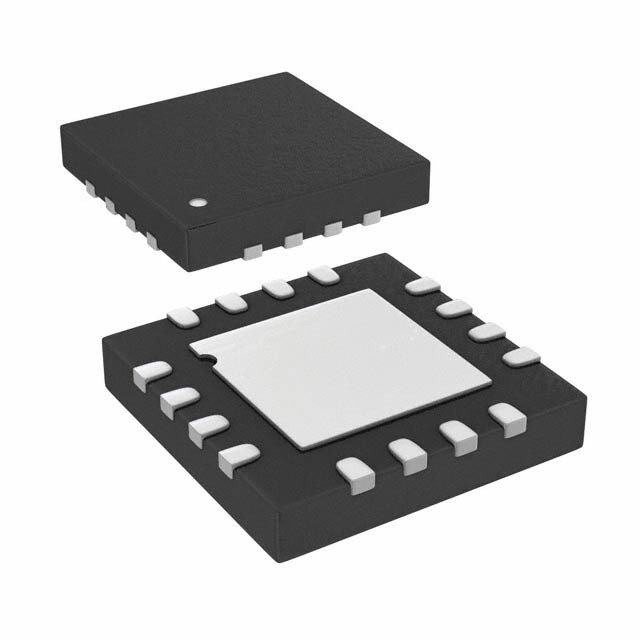
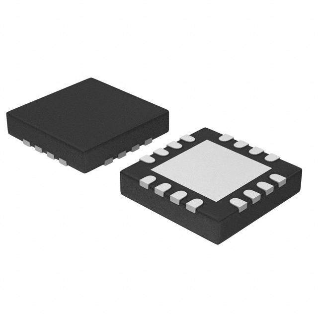
| 产品图片 |
|
| rohs | 符合RoHS无铅 / 符合限制有害物质指令(RoHS)规范要求 |
| 产品系列 | 电源管理 IC,低压差稳压器,ON Semiconductor NCP4587DMX28TCG- |
| 数据手册 | |
| 产品型号 | NCP4587DMX28TCG |
| 产品种类 | 低压差稳压器 |
| 供应商器件封装 | 6-XDFN(1.2x1.2) |
| 其它名称 | NCP4587DMX28TCGOSCT |
| 包装 | 剪切带 (CT) |
| 商标 | ON Semiconductor |
| 回动电压—最大值 | 120 mV |
| 安装类型 | 表面贴装 |
| 安装风格 | SMD/SMT |
| 封装 | Reel |
| 封装/外壳 | 6-XFDFN |
| 封装/箱体 | XDFN-6 |
| 工作温度 | -40°C ~ 85°C |
| 工厂包装数量 | 5000 |
| 最大功率耗散 | 400 mW |
| 最大工作温度 | + 85 C |
| 最大输入电压 | 5.25 V |
| 标准包装 | 1 |
| 电压-跌落(典型值) | 0.12V @ 150mA |
| 电压-输入 | 最高 5.25V |
| 电压-输出 | 2.8V |
| 电压调节准确度 | 1 % |
| 电流-输出 | 150mA |
| 电流-限制(最小值) | - |
| 稳压器拓扑 | 正,固定式 |
| 稳压器数 | 1 |
| 系列 | NCP4587 |
| 负载调节 | 20 mV |
| 输出电压 | 2.8 V |
| 输出电流 | 400 mA |


PDF Datasheet 数据手册内容提取
NCP4587 150 mA, Tri-Mode, LDO Linear Voltage Regulator The NCP4587 is a CMOS 150 mA LDO which switches to a low power mode under light current loads. The device automatically switches back to a fast response mode as the output load increases above 3 mA (typ.) or it can be placed in permanent fast mode through http://onsemi.com a mode select pin. The family is available in a variety of packages: MARKING SC−70, SOT23 and an ultra thin (0.4 mm) small 1.2 x 1.2 mm XDFN. DIAGRAMS Features • Operating Input Voltage Range: 1.4 V to 5.25 V XXX • Output Voltage Range: 0.8 to 4.0 V (Available in 0.1 V steps) XMM SC−70 • Supply current: Low Power Mode – 1.0 (cid:2)A CASE 419A 1 Fast Mode – 55 (cid:2)A Standby Mode – 0.1 (cid:2)A • Very Low Dropout: 120 mV Typ. at 150 mA (V > 2.6 V) out XX • ±1% Output Voltage Accuracy (VOUT > 2 V, TJ = 25°C) XDFN6 MM • 1 High PSRR: 70 dB at 1 kHz (Fast response mode) CASE 711AA • Line Regulation 0.02%/V Typ. • Current Fold Back Protection • XXXMM Stable with Ceramic Capacitors • Available in 1.2 x 1.2 XDFN, SC−70 and SOT23 Package SOT−23−5 1 • These are Pb−Free Devices CASE 1212 Typical Applications XX, XXX= Specific Device Code • Battery Powered Equipments MM = Date Code • Portable Communication Equipments • Cameras, Image Sensors and Camcorders ORDERING INFORMATION NCP4587x See detailed ordering and shipping information in the package VIN VOUT dimensions section on page 16 of this data sheet. VIN VOUT C1 C2 1(cid:2) CE 1(cid:2) AE GND Figure 1. Typical Application Schematic © Semiconductor Components Industries, LLC, 2012 1 Publication Order Number: February, 2012 − Rev. 3 NCP4587/D
NCP4587 AE AE VIN VOUT VIN VOUT Vref Vref Current Limit CE Current Limit CE GND GND NCP4587Hxxxx NCP4587Dxxxx Figure 2. Simplified Schematic Block Diagram PIN FUNCTION DESCRIPTION Pin No. Pin No. Pin No. XDFN SC−70 SOT23 Pin Name Description 4 4 1 VIN Input pin 2 2 2 GND Ground 3 5 3 CE Chip enable pin (active “H”) 6 3 5 VOUT Output pin 1 1 4 AE Auto Eco Pin 5 − − NC No connection ABSOLUTE MAXIMUM RATINGS Rating Symbol Value Unit Input Voltage (Note 1) VIN 6.0 V Output Voltage VOUT −0.3 to VIN + 0.3 V Chip Enable Input VCE −0.3 to 6.0 V Auto Eco Input VAE −0.3 to 6.0 V Output Current IOUT 400 mA Power Dissipation XDFN PD 400 mW Power Dissipation SC−70 380 Power Dissipation SOT23 420 Maximum Junction Temperature T 150 °C J(MAX) Storage Temperature T −55 to 125 °C STG Operation Temperature T −40 to 85 °C A ESD Capability, Human Body Model (Note 2) ESDHBM 2000 V ESD Capability, Machine Model (Note 2) ESDMM 200 V Stresses exceeding Maximum Ratings may damage the device. Maximum Ratings are stress ratings only. Functional operation above the Recommended Operating Conditions is not implied. Extended exposure to stresses above the Recommended Operating Conditions may affect device reliability. 1. Refer to ELECTRICAL CHARACTERISTIS and APPLICATION INFORMATION for Safe Operating Area. 2. This device series incorporates ESD protection and is tested by the following methods: ESD Human Body Model tested per AEC−Q100−002 (EIA/JESD22−A114) ESD Machine Model tested per AEC−Q100−003 (EIA/JESD22−A115) Latchup Current Maximum Rating tested per JEDEC standard: JESD78. http://onsemi.com 2
NCP4587 THERMAL CHARACTERISTICS Rating Symbol Value Unit Thermal Characteristics, XDFN R(cid:3)JA °C/W Thermal Resistance, Junction−to−Air 250 Thermal Characteristics, SOT23 R(cid:3)JA °C/W Thermal Resistance, Junction−to−Air 238 Thermal Characteristics, SC−70 R(cid:3)JA °C/W Thermal Resistance, Junction−to−Air 263 ELECTRICAL CHARACTERISTICS −40°C ≤ TA ≤ 85°C; VIN = VOUT(NOM) + 1 V or 2.5 V, whichever is greater; IOUT = 1 mA, CIN = COUT = 0.47 (cid:2)F, unless otherwise noted. Typical values are at TA = +25°C. Parameter Test Conditions Symbol Min Typ Max Unit Operating Input Voltage VIN 1.4 5.25 V Output Voltage TA = +25 °C, VOUT > 2 V VOUT x0.99 x1.01 V IOUT = 5 mA VOUT ≤ 2 V −20 20 mV −40°C ≤ TA ≤ 85°C, VOUT > 2 V x0.975 x1.015 V IOUT = 5 mA VOUT ≤ 2 V −50 30 mV Output Voltage Temp. TA = −40 to 85°C ±50 ppm/°C Coefficient Line Regulation VIN = VOUT + 0.5 V to IOUT = 1 mA, LineReg 0.50 %/V 5 V, VIN ≥ 1.4 V (Low Power Mode) IOUT = 10 mA, 0.02 0.20 (Fast Mode) Load Regulation IOUT = 1 mA to 10 mA VOUT > 2.0 V LineReg −1.0 1.0 % VOUT ≤ 2.0 V −20 20 mV IOUT = 10 mA to 150 mA 18 40 mV Dropout Voltage IOUT = 150 mA 0.8 V ≤ VOUT < 0.9 V VDO (Note 3) V 0.9 V ≤ VOUT < 1.0 V (Note 3) 1.0 V ≤ VOUT < 1.5 V 0.24 0.4 1.5 V ≤ VOUT < 2.6 V 0.19 0.25 2.6 V ≤ VOUT < 4.0 V 0.12 0.18 Output Current IOUT 150 mA Short Current Limit VOUT = 0 V ISC 50 mA Quiescent Current IOUT = 0 mA, VOUT ≤ 1.85 V IQ 1.0 4.0 (cid:2)A Low Power Mode (Note 4) VOUT > 1.85 V 1.5 4.0 Supply Current IOUT = 10 mA, Fast Mode IGND 55 (cid:2)A Standby Current VCE = 0 V, TJ = 25°C ISTB 0.1 1 (cid:2)A Fast Mode Switch−Over Current IOUT = light to heavy load IOUTH 8.0 mA Low Power Switch−Over IOUT = heavy to light load IOUTL 1.0 2.0 mA Current CE Pin Threshold Voltage CE Input Voltage “H” VCEH 1.0 V CE Input Voltage “L” VCEL 0.4 CE Pull Down Current ICEPD 0.1 (cid:2)A 3. VIN > 1.4 V condition is dominant against this specification 4. The value of quiescent current is excluding the pull−down current of CE and AE pin http://onsemi.com 3
NCP4587 ELECTRICAL CHARACTERISTICS −40°C ≤ TA ≤ 85°C; VIN = VOUT(NOM) + 1 V or 2.5 V, whichever is greater; IOUT = 1 mA, CIN = COUT = 0.47 (cid:2)F, unless otherwise noted. Typical values are at TA = +25°C. Parameter Test Conditions Symbol Min Typ Max Unit AE Pin Threshold Voltage AE Input Voltage “H” VAEH 1.0 V AE Input Voltage “L” VAEL 0.4 AE Pull Down Current IAEPD 0.1 (cid:2)A Power Supply Rejection Ratio VIN = VOUT + 1 V or 2.2 V whichever is higher, PSRR 70 dB (cid:4)VIN = 0.2 Vpk−pk, IOUT = 30 mA, f = 1 kHz, Fast Mode Output Noise Voltage VOUT = 1.2 V, IOUT = 30 mA, f = 10 Hz to VN 115 (cid:2)Vrms 100 kHz Low Output Nch Tr. On VIN = 4 V, VCE = 0 V RLOW 50 (cid:5) Resistance 3. VIN > 1.4 V condition is dominant against this specification 4. The value of quiescent current is excluding the pull−down current of CE and AE pin http://onsemi.com 4
NCP4587 TYPICAL CHARACTERISTICS 1.4 3.0 1.2 2.5 1.0 3.8 V 2.8 V 1.8 V 2.0 V) 0.8 VIN = 5.5 V V) (T (T 1.5 U U O 0.6 O V V 1.0 0.4 5.25 V 3.8 V 5.25 V 0.2 0.5 VIN = 5.5 V 0.0 0.0 0 50 100 150 200 250 300 350 400 0 50 100 150 200 250 300 IOUT (mA) IOUT (mA) Figure 3. Output Voltage vs. Output Current Figure 4. Output Voltage vs. Output Current 1.2 V Version (T = 25(cid:2)C) 2.8 V Version (T = 25(cid:2)C) A A 0.30 0.18 0.25 0.15 0.20 0.12 V) V) (DO0.15 25°C (DO0.09 25°C V V 0.10 85°C 0.06 85°C −40°C −40°C 0.05 0.03 0.00 0.00 0 30 60 90 120 150 0 30 60 90 120 150 IOUT (mA) IOUT (mA) Figure 5. Dropout Voltage vs. Output Current Figure 6. Dropout Voltage vs. Output Current 1.2 V Version 2.8 V Version 1.4 3.0 1.2 2.5 1.0 2.0 V) 0.8 30 mA V) (T (T 1.5 OU 0.6 1 mA OU V V 1.0 0.4 30 mA IOUT = 50 mA 1 mA 0.5 0.2 IOUT = 50 mA 0 0.0 0 1 2 3 4 5 0 1 2 3 4 5 VIN (V) VIN (V) Figure 7. Input Voltage vs. Output Voltage Figure 8. Input Voltage vs. Output Voltage 1.2 V Version 2.8 V Version http://onsemi.com 5
NCP4587 TYPICAL CHARACTERISTICS 1.24 2.84 VIN = 2.2 V 2.83 VIN = 3.8 V 1.22 2.82 2.81 V) 1.20 V) 2.80 (T (T2.79 U U O O V 1.18 V 2.78 2.77 1.16 2.76 2.75 1.14 2.74 −40 −20 0 20 40 60 80 −40 −20 0 20 40 60 80 TJ, JUNCTION TEMPERATURE (°C) TJ, JUNCTION TEMPERATURE (°C) Figure 9. Output Voltage vs. Temperature, Figure 10. Output Voltage vs. Temperature, 1.2 V Version 2.8 V Version 70 70 60 IOUT = 10 mA 60 IOUT = 10 mA 50 50 A) 40 A) 40 (cid:2) (cid:2) (D (D N 30 N 30 G G I I 20 20 10 10 IOUT = 0 mA IOUT = 0 mA 0 0 0 1 2 3 4 5 0 1 2 3 4 5 VIN (V) VIN (V) Figure 11. Supply Current vs. Input Voltage, Figure 12. Supply Current vs. Input Voltage, 1.2 V Version 2.8 V Version 160 160 140 140 120 120 100 100 A) A) (cid:2) (cid:2) (D 80 (D 80 N N G G I 60 I 60 40 Heavy to 40 Light Load Heavy to 20 Light to 20 Light Load Light to Heavy Load Heavy Load 0 0 0.1 1 10 100 1000 0.1 1 10 100 1000 IOUT (mA) IOUT (mA) Figure 13. Supply Current vs. Output Current, Figure 14. Supply Current vs. Output Current, 1.2 V Version, V = 2.2 V, V = 0 V 2.8 V Version, V = 3.8 V, V = 0 V IN AE IN AE http://onsemi.com 6
NCP4587 TYPICAL CHARACTERISTICS 3.0 3.0 2.5 2.5 2.0 2.0 A) A) (cid:2) 1.5 (cid:2) 1.5 (N (N II II 1.0 1.0 0.5 0.5 0.0 0.0 −40 −20 0 20 40 60 80 −40 −20 0 20 40 60 80 TJ, JUNCTION TEMPERATURE (°C) TJ, JUNCTION TEMPERATURE (°C) Figure 15. Supply Current vs. Temperature, Figure 16. Supply Current vs. Temperature, 1.2 Version, V = 2.2 V, V = 0 V 2.8 Version, V = 3.8 V, V = 0 V IN AE IN AE 55 55 50 50 45 45 A) A) (cid:2) 40 (cid:2) 40 (N (N II II 35 35 30 30 25 25 −40 −20 0 20 40 60 80 −40 −20 0 20 40 60 80 TJ, JUNCTION TEMPERATURE (°C) TJ, JUNCTION TEMPERATURE (°C) Figure 17. Supply Current vs. Temperature, Figure 18. Supply Current vs. Temperature, 1.2 Version, V = 2.2 V, V = 2.2 V 2.8 Version, V = 3.8 V, V = 3.8 V IN AE IN AE 100 100 90 90 80 IOUT = 30 mA IOUT = 1 mA High 80 IOUT = 30 mA IOUT = 1 mA High 70 70 R (dB) 5600 IOUT = 50 mA R (dB) 5600 IOUT = 50 mA R R S 40 S 40 P P 30 30 20 IOUT = 1 mA Low IOUT = 100 mA 20 IOUT = 1 mA Low IOUT = 100 mA 10 10 0 0 0.1 1 10 100 1000 0.1 1 10 100 1000 FREQUENCY (kHz) FREQUENCY (kHz) Figure 19. PSRR, 1.2 V Version, V = 2.2 V Figure 20. PSRR, 2.8 V Version, V = 3.8 V IN IN http://onsemi.com 7
NCP4587 TYPICAL CHARACTERISTICS 8.0 8.0 7.0 7.0 6.0 6.0 Hz)5.0 Hz) 5.0 √ √ /s /s m4.0 m 4.0 Vr Vr (cid:2) (cid:2) (N3.0 (N 3.0 V V 2.0 2.0 1.0 1.0 0 0 0.01 0.1 1 10 100 1000 0.01 0.1 1 10 100 1000 FREQUENCY (kHz) FREQUENCY (kHz) Figure 21. Output Voltage Noise, 1.2 V Version, Figure 22. Output Voltage Noise, 2.8 V Version, I = 30 mA, , V = 2.2 V I = 30 mA, V = 3.8 V OUT IN OUT IN 3.7 3.2 2.7 2.2 (V)UT 1.24 (V)N O VI V 1.22 1.20 1.18 1.16 1.14 0.0 0.2 0.4 0.6 0.8 1.0 1.2 1.4 1.6 1.8 2.0 t (ms) Figure 23. Line Transients, 1.2 V Version, t = t = 5 (cid:2)s, I = 1 mA, AE = 0 V R F OUT 5.3 4.8 4.3 3.8 (V)UT 22..8846 (V)N O VI V 2.82 2.80 2.78 2.76 2.74 0.0 0.2 0.4 0.6 0.8 1.0 1.2 1.4 1.6 1.8 2.0 t (ms) Figure 24. Line Transients, 2.8 V Version, t = t = 5 (cid:2)s, I = 1 mA, AE = 0 V R F OUT http://onsemi.com 8
NCP4587 TYPICAL CHARACTERISTICS 3.7 3.2 2.7 2.2 (V)UT1.204 (V)N O VI V1.202 1.200 1.198 1.196 1.194 0.0 0.2 0.4 0.6 0.8 1.0 1.2 1.4 1.6 1.8 2.0 t (ms) Figure 25. Line Transients, 1.2 V Version, t = t = 5 (cid:2)s, I = 30 mA, AE = V V R F OUT IN 5.3 4.8 4.3 3.8 (V)UT2.804 (V)N O VI V2.802 2.800 2.798 2.796 2.794 0.0 0.2 0.4 0.6 0.8 1.0 1.2 1.4 1.6 1.8 2.0 t (ms) Figure 26. Line Transients, 2.8 V Version, t = t = 5 (cid:2)s, I = 30 mA, AE = V V R F OUT IN 225 150 75 0 V) 1.30 A) (UT 1.25 (mT O U V 1.20 O I 1.15 1.10 1.05 1.00 0 20 40 60 80 100 120 140 160 180 200 t ((cid:2)s) Figure 27. Load Transients, 1.2 V Version, I = 1 – 150 mA, t = t = 0.5 (cid:2)s, V = 2.2 V, OUT R F IN AE = 0 V http://onsemi.com 9
NCP4587 TYPICAL CHARACTERISTICS 225 150 75 0 V) 2.90 A) (UT 2.85 (mT O U V 2.80 O I 2.75 2.70 2.65 2.60 0 20 40 60 80 100 120 140 160 180 200 t ((cid:2)s) Figure 28. Load Transients, 2.8 V Version, I = 1 – 150 mA, t = t = 0.5 (cid:2)s, V = 2.2 V, OUT R F IN AE = 0 V 225 150 75 0 V) 1.30 A) (UT 1.25 (mT O U V 1.20 O I 1.15 1.10 1.05 1.00 0 20 40 60 80 100 120 140 160 180 200 t ((cid:2)s) Figure 29. Load Transients, 1.2 V Version, I = 1 – 150 mA, t = t = 0.5 (cid:2)s, V = 2.2 V, OUT R F IN AE = V V IN 225 150 75 0 V) 2.90 A) (UT 2.85 (mT O U V 2.80 O I 2.75 2.70 2.65 2.60 0 20 40 60 80 100 120 140 160 180 200 t ((cid:2)s) Figure 30. Load Transients, 2.8 V Version, I = 1 – 150 mA, t = t = 0.5 (cid:2)s, V = 2.8 V, OUT R F IN AE = V V IN http://onsemi.com 10
NCP4587 TYPICAL CHARACTERISTICS 75 50 25 0 V) 1.24 A) (UT 1.22 (mT O U V 1.20 O I 1.18 1.16 1.14 1.12 0 20 40 60 80 100 120 140 160 180 200 t ((cid:2)s) Figure 31. Load Transients, 1.2 V Version, I = 1 – 50 mA, t = t = 0.5 (cid:2)s, V = 2.2 V, OUT R F IN AE = 0 V 75 50 25 0 V) 2.84 A) (UT 2.82 (mT O U V 2.80 O I 2.78 2.76 2.74 2.72 0 20 40 60 80 100 120 140 160 180 200 t ((cid:2)s) Figure 32. Load Transients, 2.8 V Version, I = 1 – 50 mA, t = t = 0.5 (cid:2)s, V = 3.8 V, OUT R F IN AE = 0 V 75 50 25 0 V) 1.24 A) (UT 1.22 (mT O U V 1.20 O I 1.18 1.16 1.14 1.12 0 20 40 60 80 100 120 140 160 180 200 t ((cid:2)s) Figure 33. Load Transients, 1.2 V Version, I = 1 – 50 mA, t = t = 0.5 (cid:2)s, V = 2.2 V, OUT R F IN AE = V V IN http://onsemi.com 11
NCP4587 TYPICAL CHARACTERISTICS 75 50 25 0 V) 2.84 A) (UT 2.82 (mT O U V 2.80 O I 2.78 2.76 2.74 2.72 0 20 40 60 80 100 120 140 160 180 200 t ((cid:2)s) Figure 34. Load Transients, 2.8 V Version, I = 1 – 50 mA, t = t = 0.5 (cid:2)s, V = 3.8 V, AE OUT R F IN = V V IN 150 100 50 0 V) 1.22 A) (UT 1.21 (mT O U V 1.20 O I 1.19 1.18 1.17 1.16 0 20 40 60 80 100 120 140 160 180 200 t ((cid:2)s) Figure 35. Load Transients, 1.2 V Version, I = 50 – 100 mA, t = t = 0.5 (cid:2)s, V = 2.2 V OUT R F IN 150 100 50 0 V) 2.82 A) (UT 2.81 (mT O U V 2.80 O I 2.79 2.78 2.77 2.76 0 20 40 60 80 100 120 140 160 180 200 t ((cid:2)s) Figure 36. Load Transients, 2.8 V Version, I = 50 – 100 mA, t = t = 0.5 (cid:2)s, V = 3.8 V OUT R F IN http://onsemi.com 12
NCP4587 TYPICAL CHARACTERISTICS 3 2 1 0 (V)UT 11..2212 (V)E VO 1.20 VA 1.19 1.18 1.17 1.16 0 1 2 3 4 5 6 7 8 9 10 t (ms) Figure 37. AE Switch Transients, 1.2 V Version, V = 2.2 V, I = 1 mA IN OUT 6 4 2 0 2.82 (V)UT 2.81 (V)E VO 2.80 VA 2.79 2.78 2.77 2.76 0 1 2 3 4 5 6 7 8 9 10 t (ms) Figure 38. AE Switch Transients, 2.8 V Version, V = 3.8 V, I = 1 mA IN OUT 3 2 Chip Enable 1 0 V) V) V (OUT 1.5 IOUT = 150 mA V (CE 1.0 IOUT = 1 mA 0.5 IOUT = 30 mA 0.0 −0.5 0 10 20 30 40 50 60 70 80 90 100 t ((cid:2)s) Figure 39. Start-up, 1.2 V Version, V = 2.0 V IN http://onsemi.com 13
NCP4587 TYPICAL CHARACTERISTICS 6 4 Chip Enable 2 0 V) V) V (OUT 3.0 IOUT = 150 mA V (CE IOUT = 1 mA 2.0 1.0 IOUT = 30 mA 0.0 −1.0 0 10 20 30 40 50 60 70 80 90 100 t ((cid:2)s) Figure 40. Start-up, 2.8 V Version, V =3.8 V IN 3 2 1 Chip Enable 0 V) V) V (OUT 1.5 IOUT = 1 mA V (CE IOUT = 30 mA 1.0 IOUT = 150 mA 0.5 0.0 −0.5 0.0 0.1 0.2 0.3 0.4 0.5 0.6 0.7 0.8 0.9 1.0 t (ms) Figure 41. Shutdown, 1.2 V Version, V = 2.2 V IN 6 4 2 Chip Enable 0 V) V) V (OUT 3.0 IOUT = 1 mA IOUT = 30 mA V (CE 2.0 IOUT = 150 mA 1.0 0.0 −1.0 0.0 0.1 0.2 0.3 0.4 0.5 0.6 0.7 0.8 0.9 1.0 t (ms) Figure 42. Shutdown, 2.8 V Version, V = 3.8 V IN http://onsemi.com 14
NCP4587 APPLICATION INFORMATION A typical application circuit for NCP4587 series is shown current capability in normal operation, but when over in Figure 43. current occurs, the output voltage and current decrease until the over current condition ends. Typical characteristics of NCP4587x this protection type can be observed in the Output Voltage VIN VOUT versus Output Current graphs shown in the typical VIN VOUT characteristics chapter of this datasheet. C1 C2 1(cid:2) CE 1(cid:2) Output Discharger AE The D version includes a transistor between VOUT and GND GND that is used for faster discharging of the output capacitor. This function is activated when the IC goes into disable mode. Auto ECO and Fast Mode The NCP4587 has two operation modes that have impact Figure 43. Typical Application Schematic on supply current and transient response at low output current. These two modes can be selected by AE pin. If AE pin is at low level or floating Auto ECO mode is available. Input Decoupling Capacitor (C1) A 1 (cid:2)F ceramic input decoupling capacitor should be Please, see supply current vs. output current charts. If AE pin connected as close as possible to the input and ground pin of is at high level the device works in permanent Fast Transient the NCP4587. Higher values and lower ESR improves line Mode. transient response. Thermal As power across the IC increases, it might become Output Decoupling Capacitor (C2) A 1 (cid:2)F ceramic output decoupling capacitor is sufficient necessary to provide some thermal relief. The maximum to achieve stable operation of the IC. If tantalum capacitor power dissipation supported by the device is dependent is used, and its ESR is high, the loop oscillation may result. upon board design and layout. Mounting pad configuration If output capacitor is composed from few ceramic capacitors on the PCB, the board material, and also the ambient in parallel, the operation can be unstable. The capacitor temperature affect the rate of temperature rise for the part. should be connected as close as possible to the output and That is to say, when the device has good thermal ground pin. Larger values and lower ESR improves dynamic conductivity through the PCB, the junction temperature will parameters. be relatively low with high power dissipation applications. Enable Operation PCB layout Enable pin CE may be used for turning the regulator on Make VIN and GND line sufficient. If their impedance is and off. The regulator is switched on when CE pin voltage high, noise pickup or unstable operation may result. Connect is above logic high level. Enable pin has internal pull down capacitors C1 and C2 as close as possible to the IC, and make current source. If enable function is not needed connect CE wiring as short as possible. pin to VIN. Current Limit This regulator includes fold-back type current limit circuit. This type of protection doesn’t limit current up to http://onsemi.com 15
NCP4587 ORDERING INFORMATION Nominal Output Device Voltage Description Marking Package Shipping† NCP4587DMX12TCG 1.2 V Auto discharge YE XDFN 5000 / Tape & Reel (Pb−Free) NCP4587DMX18TCG 1.8 V Auto discharge YL XDFN 5000 / Tape & Reel (Pb−Free) NCP4587DMX28TCG 2.8 V Auto discharge YW XDFN 5000 / Tape & Reel (Pb−Free) NCP4587DMX30TCG 3.0 V Auto discharge YY XDFN 5000 / Tape & Reel (Pb−Free) NCP4587DMX31TCG 3.1 V Auto discharge YZ XDFN 5000 / Tape & Reel (Pb−Free) NCP4587DMX33TCG 3.3 V Auto discharge ZB XDFN 5000 / Tape & Reel (Pb−Free) NCP4587DSN12T1G 1.2 V Auto discharge DBE SOT−23 3000 / Tape & Reel (Pb−Free) NCP4587DSN18T1G 1.8 V Auto discharge DBL SOT−23 3000 / Tape & Reel (Pb−Free) NCP4587DSN28T1G 2.8 V Auto discharge DBW SOT−23 3000 / Tape & Reel (Pb−Free) NCP4587DSN30T1G 3.0 V Auto discharge DBY SOT−23 3000 / Tape & Reel (Pb−Free) NCP4587DSN33T1G 3.3 V Auto discharge EBB SOT−23 3000 / Tape & Reel (Pb−Free) †For information on tape and reel specifications, including part orientation and tape sizes, please refer to our Tape and Reel Packaging Specifications Brochure, BRD8011/D. NOTE: To order other package and voltage variants, please contact your ON Semiconductor sales representative. http://onsemi.com 16
NCP4587 PACKAGE DIMENSIONS SC−88A (SC−70−5/SOT−353) CASE 419A−02 ISSUE K A NOTES: 1. DIMENSIONING AND TOLERANCING G PER ANSI Y14.5M, 1982. 2. CONTROLLING DIMENSION: INCH. 3. 419A−01 OBSOLETE. NEW STANDARD 419A−02. 4. DIMENSIONS A AND B DO NOT INCLUDE 5 4 MOLD FLASH, PROTRUSIONS, OR GATE BURRS. S −B− INCHES MILLIMETERS 1 2 3 DIM MIN MAX MIN MAX A 0.071 0.087 1.80 2.20 B 0.045 0.053 1.15 1.35 C 0.031 0.043 0.80 1.10 D 0.004 0.012 0.10 0.30 D 5 PL 0.2 (0.008) M B M G 0.026 BSC 0.65 BSC H --- 0.004 --- 0.10 J 0.004 0.010 0.10 0.25 N K 0.004 0.012 0.10 0.30 N 0.008 REF 0.20 REF S 0.079 0.087 2.00 2.20 J C K H http://onsemi.com 17
NCP4587 PACKAGE DIMENSIONS XDFN6 1.2x1.2, 0.4P CASE 711AA−01 ISSUE O NOTES: D A 1. DIMENSIONING AND TOLERANCING PER B ASME Y14.5M, 1994. 2. CONTROLLING DIMENSION: MILLIMETERS. 3. DIMENSION b APPLIES TO PLATED TERMINAL AND IS MEASURED BETWEEN 0.15 AND 0.25mm FROM TERMINAL TIPS. ÍÍÍ 4. COPLANARITY APPLIES TO ALL OF THE PIN ONE E TERMINALS. REFERENCE ÍÍÍ MILLIMETERS DIM MIN MAX 2X 0.05 CÍÍÍ A --- 0.40 A1 0.00 0.05 b 0.13 0.23 2X 0.05 C TOP VIEW C 0.20 0.30 D 1.20 BSC E 1.20 BSC e 0.40 BSC A L 0.37 0.48 0.05 C RECOMMENDED 0.05 C A1 MOUNTING FOOTPRINT* NOTE 4 SIDE VIEW C SPELAATNIENG 6X 6X 0.22 0.66 PACKAGE e OUTLINE 1 3 1.50 C 6XL 0.40 PITCH DIMENSIONS: MILLIMETERS 6 4 6X b *For additional information on our Pb−Free strategy and soldering 0.05 M C A B details, please download the ON Semiconductor Soldering and Mounting Techniques Reference Manual, SOLDERRM/D. BOTTOM VIEW NOTE 3 http://onsemi.com 18
NCP4587 PACKAGE DIMENSIONS SOT−23 CASE 1212−01 ISSUE A NOTES: A 1. DIMENSIONING AND TOLERANCING PER ASME Y14.5M, 1994. A D B A2 2. CONTROLLING DIMENSIONS: MILLIMETERS. 0.05 S A1 3. DATUM C IS THE SEATING PLANE. MILLIMETERS 5 4 DIM MIN MAX E L A --- 1.45 1 2 3 A1 0.00 0.10 E1 A2 1.00 1.30 L1 5Xb C b 0.30 0.50 c 0.10 0.25 e 0.10 M C B S A S C D 2.70 3.10 E 2.50 3.10 E1 1.50 1.80 e 0.95 BSC L 0.20 --- L1 0.45 0.75 RECOMMENDED SOLDERING FOOTPRINT* 3.30 5X 0.85 5X 0.56 0.95 PITCH DIMENSIONS: MILLIMETERS *For additional information on our Pb−Free strategy and soldering details, please download the ON Semiconductor Soldering and Mounting Techniques Reference Manual, SOLDERRM/D. ON Semiconductor and are registered trademarks of Semiconductor Components Industries, LLC (SCILLC). SCILLC reserves the right to make changes without further notice to any products herein. SCILLC makes no warranty, representation or guarantee regarding the suitability of its products for any particular purpose, nor does SCILLC assume any liability arising out of the application or use of any product or circuit, and specifically disclaims any and all liability, including without limitation special, consequential or incidental damages. “Typical” parameters which may be provided in SCILLC data sheets and/or specifications can and do vary in different applications and actual performance may vary over time. All operating parameters, including “Typicals” must be validated for each customer application by customer’s technical experts. SCILLC does not convey any license under its patent rights nor the rights of others. SCILLC products are not designed, intended, or authorized for use as components in systems intended for surgical implant into the body, or other applications intended to support or sustain life, or for any other application in which the failure of the SCILLC product could create a situation where personal injury or death may occur. Should Buyer purchase or use SCILLC products for any such unintended or unauthorized application, Buyer shall indemnify and hold SCILLC and its officers, employees, subsidiaries, affiliates, and distributors harmless against all claims, costs, damages, and expenses, and reasonable attorney fees arising out of, directly or indirectly, any claim of personal injury or death associated with such unintended or unauthorized use, even if such claim alleges that SCILLC was negligent regarding the design or manufacture of the part. SCILLC is an Equal Opportunity/Affirmative Action Employer. This literature is subject to all applicable copyright laws and is not for resale in any manner. PUBLICATION ORDERING INFORMATION LITERATURE FULFILLMENT: N. American Technical Support: 800−282−9855 Toll Free ON Semiconductor Website: www.onsemi.com Literature Distribution Center for ON Semiconductor USA/Canada P.O. Box 5163, Denver, Colorado 80217 USA Europe, Middle East and Africa Technical Support: Order Literature: http://www.onsemi.com/orderlit Phone: 303−675−2175 or 800−344−3860 Toll Free USA/Canada Phone: 421 33 790 2910 Fax: 303−675−2176 or 800−344−3867 Toll Free USA/Canada Japan Customer Focus Center For additional information, please contact your local Email: orderlit@onsemi.com Phone: 81−3−5817−1050 Sales Representative http://onsemi.com NCP4587/D 19