ICGOO在线商城 > 集成电路(IC) > PMIC - 稳压器 - 线性 > LDK130PU33R
 Datasheet下载
- 型号: LDK130PU33R
- 制造商: STMicroelectronics
- 库位|库存: xxxx|xxxx
- 要求:
| 数量阶梯 | 香港交货 | 国内含税 |
| +xxxx | $xxxx | ¥xxxx |
查看当月历史价格
查看今年历史价格
LDK130PU33R产品简介:
ICGOO电子元器件商城为您提供LDK130PU33R由STMicroelectronics设计生产,在icgoo商城现货销售,并且可以通过原厂、代理商等渠道进行代购。 LDK130PU33R价格参考。STMicroelectronicsLDK130PU33R封装/规格:PMIC - 稳压器 - 线性, Linear Voltage Regulator IC Positive Fixed 1 Output 3.3V 300mA 6-DFN (1.2x1.3)。您可以下载LDK130PU33R参考资料、Datasheet数据手册功能说明书,资料中有LDK130PU33R 详细功能的应用电路图电压和使用方法及教程。
STMicroelectronics的LDK130PU33R是一款低功耗、低压差线性稳压器,广泛应用于对电源管理有较高要求的场景。其主要应用场景包括但不限于以下几个方面:

 1. 便携式电子设备
   LDK130PU33R具有低静态电流(典型值为2.5μA),非常适合用于电池供电的便携式设备,如智能手机、平板电脑、可穿戴设备等。这些设备通常需要长时间保持待机状态,因此低功耗特性可以有效延长电池寿命。

 2. 物联网(IoT)设备
   在物联网应用中,许多传感器和通信模块需要稳定且低功耗的电源供应。LDK130PU33R能够为这些模块提供稳定的电压输出(3.3V),并且其低压差特性可以在输入电压接近输出电压时仍能正常工作,适合在电池供电或能量收集系统中使用。

 3. 工业自动化与控制
   工业环境中,许多传感器、执行器和其他嵌入式系统需要可靠的电源管理。LDK130PU33R的高精度输出电压(±2%)和良好的瞬态响应性能,使其能够在工业自动化设备中提供稳定的电源支持,确保系统的可靠性和稳定性。

 4. 消费类电子产品
   在消费类电子产品中,如智能家居设备、无线耳机、智能音箱等,LDK130PU33R可以为微控制器、传感器、通信模块等提供稳定的电源。其小封装尺寸(SOT-23-5)使得它非常适合用于空间受限的设计。

 5. 医疗设备
   医疗设备如血糖仪、体温计、心率监测器等,通常要求电源管理芯片具备高精度和低功耗的特点。LDK130PU33R的低噪声输出和高精度电压输出,能够为这些设备提供稳定的电源,确保测量结果的准确性。

 6. 汽车电子
   虽然LDK130PU33R不是专门为汽车设计的,但在一些非关键的车载应用中,如车内娱乐系统、传感器模块等,它仍然可以提供可靠的电源管理功能。

总之,LDK130PU33R凭借其低功耗、低压差、高精度等特点,适用于多种需要稳定电源管理和长电池寿命的应用场景。
| 参数 | 数值 |
| 产品目录 | 集成电路 (IC)半导体 |
| 描述 | IC REG LDO 3.3V 0.3A 6DFN低压差稳压器 300mA current very low noise LDO |
| 产品分类 | |
| 品牌 | STMicroelectronics |
| 产品手册 | |
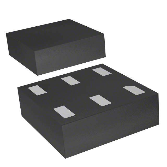
| 产品图片 |
|
| rohs | 符合RoHS无铅 / 符合限制有害物质指令(RoHS)规范要求 |
| 产品系列 | 电源管理 IC,低压差稳压器,STMicroelectronics LDK130PU33R- |
| mouser_ship_limit | 该产品可能需要其他文件才能进口到中国。 |
| 数据手册 | |
| 产品型号 | LDK130PU33R |
| PSRR/纹波抑制—典型值 | 55 dB |
| 产品 | LDO Regulators |
| 产品种类 | 低压差稳压器 |
| 供应商器件封装 | 6-DFN (1.2x1.3) |
| 其它名称 | 497-14261-2 |
| 包装 | 带卷 (TR) |
| 商标 | STMicroelectronics |
| 回动电压—最大值 | 400 mV |
| 安装类型 | 表面贴装 |
| 安装风格 | SMD/SMT |
| 封装 | Reel |
| 封装/外壳 | 6-XFDFN |
| 封装/箱体 | DFN-6 |
| 工作温度 | -40°C ~ 125°C |
| 工厂包装数量 | 5000 |
| 最大功率耗散 | Internally Limited |
| 最大工作温度 | + 125 C |
| 最大输入电压 | 5.5 V |
| 最小工作温度 | + 40 C |
| 最小输入电压 | 1.9 V |
| 标准包装 | 3,000 |
| 电压-跌落(典型值) | - |
| 电压-输入 | 最高 5.5V |
| 电压-输出 | 3.3V |
| 电压调节准确度 | 2 % |
| 电流-输出 | 300mA |
| 电流-限制(最小值) | - |
| 电源电流 | 70 uA |
| 稳压器拓扑 | 正,固定式 |
| 稳压器数 | 1 |
| 类型 | Low Quiescent Current |
| 系列 | LDK130P |
| 线路调整率 | 0.05 %/ V |
| 负载调节 | 0.006 % / mA |
| 输出电压 | 3.3 V |
| 输出电压容差 | 2 % |
| 输出电流 | 300 mA |
| 输出端数量 | 1 Output |
| 输出类型 | Fixed |


- 商务部:美国ITC正式对集成电路等产品启动337调查
- 曝三星4nm工艺存在良率问题 高通将骁龙8 Gen1或转产台积电
- 太阳诱电将投资9.5亿元在常州建新厂生产MLCC 预计2023年完工
- 英特尔发布欧洲新工厂建设计划 深化IDM 2.0 战略
- 台积电先进制程称霸业界 有大客户加持明年业绩稳了
- 达到5530亿美元!SIA预计今年全球半导体销售额将创下新高
- 英特尔拟将自动驾驶子公司Mobileye上市 估值或超500亿美元
- 三星加码芯片和SET,合并消费电子和移动部门,撤换高东真等 CEO
- 三星电子宣布重大人事变动 还合并消费电子和移动部门
- 海关总署:前11个月进口集成电路产品价值2.52万亿元 增长14.8%


PDF Datasheet 数据手册内容提取
LDK130 300 mA low quiescent current very low noise LDO (automotive for SOT23-5L package) Datasheet - production data Applications • Mobile phones • Portable consumer and industrial devices • Cordless phones and similar battery-powered systems (cid:54)(cid:50)(cid:55)(cid:21)(cid:22)(cid:16)(cid:24)(cid:47) (cid:39)(cid:41)D(cid:49)F(cid:25)N(cid:3)(cid:11)6(cid:20)(cid:17) (cid:21)1(cid:3).(cid:91)2(cid:3)x(cid:20)1(cid:17)(cid:22).3(cid:3)(cid:80)(cid:80)(cid:12) • Automotive P.O.L. • A.D.A.S. Description (cid:54)(cid:50)(cid:55)(cid:22)(cid:21)(cid:22)(cid:16)(cid:24)(cid:47) The LDK130 low drop voltage regulator provides 300 mA of maximum current from an input supply voltage in the range of 1.9 V to 5.5 V, with a typical dropout voltage of 100 mV. Features It is stabilized with a ceramic capacitor on the output. • AEC-Q100 qualified (automotive grade 1, SOT23-5L package) The very low drop voltage, low quiescent current • Input voltage from 1.9 to 5.5 V and low-noise features make it suitable for low- power battery-powered applications. • Very low-dropout voltage (100 mV typ. at 100 mA load) An enable logic control function puts the LDK130 in shutdown mode allowing a total current • Low quiescent current (typ. 30 µA, 1 µA in OFF consumption lower than 1 µA. mode) • Very low noise The device also includes short-circuit constant current limiting and thermal protection. • Output voltage tolerance: ± 2.0% at 25 °C • 300 mA guaranteed output current • Wide range of fixed output voltages available on request: from 0.8 V to 3.5 V with 100 mV step • Adjustable version: from 0.8 V to V - V IN drop • Logic-controlled electronic shutdown • Compatible with ceramic capacitor C = 1 µF OUT • Internal current and thermal limit • Available in SOT23-5L, SOT323-5L and DFN6 1.2x1.3 packages • Temperature range: -40 °C to 125 °C January 2018 DocID024210 Rev 6 1/27 This is information on a product in full production. www.st.com
Contents LDK130 Contents 1 Block diagram . . . . . . . . . . . . . . . . . . . . . . . . . . . . . . . . . . . . . . . . . . . . . . 5 2 Pin configuration . . . . . . . . . . . . . . . . . . . . . . . . . . . . . . . . . . . . . . . . . . . . 6 3 Typical application . . . . . . . . . . . . . . . . . . . . . . . . . . . . . . . . . . . . . . . . . . 7 4 Maximum ratings . . . . . . . . . . . . . . . . . . . . . . . . . . . . . . . . . . . . . . . . . . . . 8 5 Electrical characteristics . . . . . . . . . . . . . . . . . . . . . . . . . . . . . . . . . . . . . 9 6 Typical performance characteristics . . . . . . . . . . . . . . . . . . . . . . . . . . . 11 7 Package information . . . . . . . . . . . . . . . . . . . . . . . . . . . . . . . . . . . . . . . . 17 7.1 SOT23-5L package information . . . . . . . . . . . . . . . . . . . . . . . . . . . . . . . . 17 7.2 DFN6 1.2 x 1.3 package information . . . . . . . . . . . . . . . . . . . . . . . . . . . . 19 7.3 SOT323-5L package information . . . . . . . . . . . . . . . . . . . . . . . . . . . . . . . 21 7.4 Packing information . . . . . . . . . . . . . . . . . . . . . . . . . . . . . . . . . . . . . . . . . 23 7.5 SOT23-5L and SOT323-5L packing information . . . . . . . . . . . . . . . . . . . 23 8 Order code . . . . . . . . . . . . . . . . . . . . . . . . . . . . . . . . . . . . . . . . . . . . . . . . 25 9 Revision history . . . . . . . . . . . . . . . . . . . . . . . . . . . . . . . . . . . . . . . . . . . 26 2/27 DocID024210 Rev 6
LDK130 List of tables List of tables Table 1. Pin description (SOT23-5L, SOT323-5L) . . . . . . . . . . . . . . . . . . . . . . . . . . . . . . . . . . . . . . . 6 Table 2. Absolute maximum ratings. . . . . . . . . . . . . . . . . . . . . . . . . . . . . . . . . . . . . . . . . . . . . . . . . . 8 Table 3. Thermal data. . . . . . . . . . . . . . . . . . . . . . . . . . . . . . . . . . . . . . . . . . . . . . . . . . . . . . . . . . . . . 8 Table 4. Electrical characteristics for LDK130 (fixed version). . . . . . . . . . . . . . . . . . . . . . . . . . . . . . . 9 Table 5. Electrical characteristics for LDK130(adjustable version) . . . . . . . . . . . . . . . . . . . . . . . . . 10 Table 6. SOT23-5L package mechanical data. . . . . . . . . . . . . . . . . . . . . . . . . . . . . . . . . . . . . . . . . 18 Table 7. DFN6 1.2 x 1.3 package mechanical data . . . . . . . . . . . . . . . . . . . . . . . . . . . . . . . . . . . . . 20 Table 8. SOT323-5L mechanical data . . . . . . . . . . . . . . . . . . . . . . . . . . . . . . . . . . . . . . . . . . . . . . . 22 Table 9. SOT23-5L tape and reel mechanical data . . . . . . . . . . . . . . . . . . . . . . . . . . . . . . . . . . . . . 24 Table 10. SOT323-5L tape and reel mechanical data . . . . . . . . . . . . . . . . . . . . . . . . . . . . . . . . . . . . 24 Table 11. Order code . . . . . . . . . . . . . . . . . . . . . . . . . . . . . . . . . . . . . . . . . . . . . . . . . . . . . . . . . . . . . 25 Table 12. Marking. . . . . . . . . . . . . . . . . . . . . . . . . . . . . . . . . . . . . . . . . . . . . . . . . . . . . . . . . . . . . . . . 25 Table 13. Document revision history . . . . . . . . . . . . . . . . . . . . . . . . . . . . . . . . . . . . . . . . . . . . . . . . . 26 DocID024210 Rev 6 3/27 27
List of figures LDK130 List of figures Figure 1. Block diagram. . . . . . . . . . . . . . . . . . . . . . . . . . . . . . . . . . . . . . . . . . . . . . . . . . . . . . . . . . . . 5 Figure 2. Pin connections (top view) . . . . . . . . . . . . . . . . . . . . . . . . . . . . . . . . . . . . . . . . . . . . . . . . . . 6 Figure 3. Typical application circuits for fixed version . . . . . . . . . . . . . . . . . . . . . . . . . . . . . . . . . . . . . 7 Figure 4. Typical application circuits for adjustable version. . . . . . . . . . . . . . . . . . . . . . . . . . . . . . . . . 7 Figure 5. Output voltage vs. temp. for adjustable (I = 1 mA). . . . . . . . . . . . . . . . . . . . . . . . . . . . . . 11 O Figure 6. Output voltage vs. temp. for adjustable version (I = 300 mA). . . . . . . . . . . . . . . . . . . . . . 11 O Figure 7. Output voltage vs. temp. for fixed version (I = 1 mA). . . . . . . . . . . . . . . . . . . . . . . . . . . . 11 O Figure 8. Output voltage vs. temp. for fixed version (I = 300 mA). . . . . . . . . . . . . . . . . . . . . . . . . . 11 O Figure 9. Line regulation vs. temp. for adjustable version. . . . . . . . . . . . . . . . . . . . . . . . . . . . . . . . . 12 Figure 10. Short-circuit current vs. temp. for adjustable version . . . . . . . . . . . . . . . . . . . . . . . . . . . . . 12 Figure 11. Load regulation vs. temp. for adjustable version . . . . . . . . . . . . . . . . . . . . . . . . . . . . . . . . 12 Figure 12. Load regulation vs. temp. for fixed version. . . . . . . . . . . . . . . . . . . . . . . . . . . . . . . . . . . . . 12 Figure 13. Enable pin thresholds vs. temp. (V = 1.9 V). . . . . . . . . . . . . . . . . . . . . . . . . . . . . . . . . . . 12 IN Figure 14. Enable pin thresholds vs. temp. . . . . . . . . . . . . . . . . . . . . . . . . . . . . . . . . . . . . . . . . . . . . . 12 Figure 15. Quiescent current vs. temp. for adjustable version (I = 0 mA) . . . . . . . . . . . . . . . . . . . . . 13 O Figure 16. Quiescent current vs. temp. for adjustable version (I = 300 mA) . . . . . . . . . . . . . . . . . . . 13 O Figure 17. Quiescent current vs. temp. for fixed version (I = 0 mA) . . . . . . . . . . . . . . . . . . . . . . . . . 13 O Figure 18. Quiescent current vs. temp. for fixed version (I = 300 mA) . . . . . . . . . . . . . . . . . . . . . . . 13 O Figure 19. Shutdown current vs. temperature . . . . . . . . . . . . . . . . . . . . . . . . . . . . . . . . . . . . . . . . . . . 13 Figure 20. SVR vs. frequency (V = 2.5 V) . . . . . . . . . . . . . . . . . . . . . . . . . . . . . . . . . . . . . . . . . . . . . 13 O Figure 21. SVR vs. frequency (V = V ) . . . . . . . . . . . . . . . . . . . . . . . . . . . . . . . . . . . . . . . . . . . . . 14 O ADJ Figure 22. Output noise vs. frequency (V =3.3V). . . . . . . . . . . . . . . . . . . . . . . . . . . . . . . . . . . . . . . 14 O Figure 23. Output noise vs. frequency (V =V ). . . . . . . . . . . . . . . . . . . . . . . . . . . . . . . . . . . . . . . 14 O ADJ Figure 24. Stability region vs. COUT (fixed) . . . . . . . . . . . . . . . . . . . . . . . . . . . . . . . . . . . . . . . . . . . . 14 Figure 25. Stability region vs COUT (adjust.) . . . . . . . . . . . . . . . . . . . . . . . . . . . . . . . . . . . . . . . . . . . 14 Figure 26. Line transient (V = V ) . . . . . . . . . . . . . . . . . . . . . . . . . . . . . . . . . . . . . . . . . . . . . . . 14 OUT ADJ Figure 27. Line transient (V = 3 V). . . . . . . . . . . . . . . . . . . . . . . . . . . . . . . . . . . . . . . . . . . . . . . . . 15 OUT Figure 28. Load transient (V = 3 V) . . . . . . . . . . . . . . . . . . . . . . . . . . . . . . . . . . . . . . . . . . . . . . . . 15 OUT Figure 29. Load transient (V = V ). . . . . . . . . . . . . . . . . . . . . . . . . . . . . . . . . . . . . . . . . . . . . . . 15 OUT ADJ Figure 30. Startup transient. . . . . . . . . . . . . . . . . . . . . . . . . . . . . . . . . . . . . . . . . . . . . . . . . . . . . . . . . 15 Figure 31. Enable transient (V = V ) . . . . . . . . . . . . . . . . . . . . . . . . . . . . . . . . . . . . . . . . . . . . . 16 OUT ADJ Figure 32. Enable transient (V = 3 V). . . . . . . . . . . . . . . . . . . . . . . . . . . . . . . . . . . . . . . . . . . . . . . 16 OUT Figure 33. Dropout voltage vs. temperature (I = 100 mA) . . . . . . . . . . . . . . . . . . . . . . . . . . . . . . . 16 OUT Figure 34. Dropout voltage vs. temperature (I = 300 mA) . . . . . . . . . . . . . . . . . . . . . . . . . . . . . . . 16 OUT Figure 35. SOT23-5L package outline. . . . . . . . . . . . . . . . . . . . . . . . . . . . . . . . . . . . . . . . . . . . . . . . . 17 Figure 36. SOT23-5L footprint (dimensions in mm). . . . . . . . . . . . . . . . . . . . . . . . . . . . . . . . . . . . . . . 18 Figure 37. DFN6 1.2 x 1.3 package outline. . . . . . . . . . . . . . . . . . . . . . . . . . . . . . . . . . . . . . . . . . . . . 19 Figure 38. DFN6 1.2 x 1.3 recommended footprint (dimensions in mm). . . . . . . . . . . . . . . . . . . . . . . 20 Figure 39. SOT323-5L package outline. . . . . . . . . . . . . . . . . . . . . . . . . . . . . . . . . . . . . . . . . . . . . . . . 21 Figure 40. SOT23-5L and SOT323-5L tape and reel outline. . . . . . . . . . . . . . . . . . . . . . . . . . . . . . . . 23 4/27 DocID024210 Rev 6
LDK130 Block diagram 1 Block diagram Figure 1. Block diagram DocID024210 Rev 6 5/27 27
Pin configuration LDK130 2 Pin configuration Figure 2. Pin connections (top view) SOT23-5L, SOT323-5L DFN6 1.2 x 1.3 Table 1. Pin description (SOT23-5L, SOT323-5L) Pin Symbol Function SOT23/ DFN6 SOT323 1 6 IN Input voltage of the LDO 2 2 GND Common ground 3 4 EN Enable pin logic input: low = shutdown, high = active 4 3 BYP(1)/ADJ Bypass capacitor on fixed versions, adjustable pin on ADJ versions 5 1 OUT Output voltage of the LDO - 5 N/C Not connected. This pin should be connected to GND 1. Bypass capacitor for noise reduction on fixed version is optional, if not used the relevant pin must be left floating with no routing on the board. 6/27 DocID024210 Rev 6
LDK130 Typical application 3 Typical application Figure 3. Typical application circuits for fixed version Figure 4. Typical application circuits for adjustable version V = V (1 + R / R ) O ADJ 1 2 DocID024210 Rev 6 7/27 27
Maximum ratings LDK130 4 Maximum ratings Table 2. Absolute maximum ratings Symbol Parameter Value Unit V DC input voltage - 0.3 to 7 V IN V DC output voltage - 0.3 to V + 0.3 V OUT I V Enable input voltage - 0.3 to V + 0.3 V EN I V ADJ/bypass pin voltage 2 V BYP/ADJ I Output current Internally limited mA OUT P Power dissipation Internally limited mW D T Storage temperature range - 65 to 150 °C STG T Operating junction temperature range - 40 to 125 °C OP Note: Absolute maximum ratings are those values beyond which damage to the device may occur. Functional operation under these conditions is not implied. All values are referred to GND. Table 3. Thermal data Symbol Parameter SOT23-5L SOT323-5L DFN6 Unit R Thermal resistance junction ambient 160 246 237 °C/W thJA R Thermal resistance junction case 68 134 104 °C/W thJC 8/27 DocID024210 Rev 6
LDK130 Electrical characteristics 5 Electrical characteristics T = 25 °C, V = V + 1 V, C = C = 1 µF, I = 1 mA, V = V , unless J IN OUT(NOM) IN OUT OUT EN IN otherwise specified. Table 4. Electrical characteristics for LDK130 (fixed version) Symbol Parameter Test conditions Min. Typ. Max. Unit V Operating input voltage - 1.9 - 5.5 V IN I = 1 mA, T = 25 °C -2.0 - 2.0 % OUT J V V accuracy OUT OUT I = 1 mA, -40 °C < T < 125 °C -3.0 - 3.0 % OUT J ΔV Static line regulation V +1 V ≤ V ≤ 5.5 V, I = 1 mA - 0.05 - %/V OUT OUT IN OUT ΔV Static load regulation I = 1 mA to 300 mA - 0.006 - %/mA OUT OUT I = 100 mA, V = 2.5 V - 100 - OUT OUT VDROP Dropout voltage(1) IOUT = 300 mA, VOUT = 2.5 V - 200 400 mV 40 °C < T < 125 °C J 10 Hz to 100 kHz, I = 10 mA, e Output noise voltage OUT - 51 - µV /V N V = 2.5 V, C = 10 nF RMS OUT BYP V = V +0.5 V ± V Supply voltage IN OUTNOM RIPPLE SVR V = 0.1 V freq. = 120 Hz to 10 kHz - 55 - dB rejection RIPPLE I = 10 mA OUT I = 0 mA, -40 °C < T < 125 °C - 30 60 OUT J I Quiescent current I = 300 mA, -40 °C < T < 125 °C - 70 120 µA Q OUT J V input current in OFF mode: V = GND - - 1 IN EN I Short-circuit current R = 0 - 450 - mA SC L Enable input logic low V = 1.9 V to 5.5 V, -40 °C < T < 125 °C - - 0.4 IN J V V EN Enable input logic high V = 1.9 V to 5.5 V, -40 °C < T < 125 °C 1.2 - IN J I Enable pin input current V = V - - 100 nA EN SHDN IN Thermal shutdown - - 160 - T °C SHDN Hysteresis - - 20 - Capacitance (see Section6: Typical C Output capacitor 1 - 22 µF OUT performance characteristics) 1. Dropout voltage is the input-to-output voltage difference at which the output voltage is 100 mV below its nominal value. DocID024210 Rev 6 9/27 27
Electrical characteristics LDK130 T = 25 °C, V = V + 1 V, C = C = 1 µF, I = 1 mA, V = V , unless J IN OUT(NOM) IN OUT OUT EN IN otherwise specified. Table 5. Electrical characteristics for LDK130(adjustable version) Symbol Parameter Test conditions Min. Typ. Max. Unit V Operating input voltage 1.9 - 5.5 V IN I =1 mA, T = 25 °C 784 800 816 mV OUT J V V accuracy ADJ ADJ I = 1 mA, -40 °C < T < 125 °C -3.0 3.0 % OUT J ΔV Static line regulation V +1 V ≤ V ≤ 5.5 V, I = 1 mA - 0.05 - %/V OUT OUT IN OUT ΔV Static load regulation I = 1 mA to 300 mA - 0.006 - %/mA OUT OUT I = 100 mA, V = 2.5 V - 100 - OUT OUT VDROP Dropout voltage(1) IOUT = 300 mA, VOUT = 2.5 V - 200 400 mV 40 °C < T < 125 °C J e Output noise voltage 10 Hz to 100 kHz, I = 10 mA - 130 - µV /V N OUT RMS I Adjust pin current - - 1 µA ADJ V = V +0.5 V ± V Supply voltage IN OUTNOM RIPPLE SVR V = 0.1 V freq. = 120 Hz to 10 kHz - 55 dB rejection RIPPLE I = 10 mA OUT I = 0 mA, -40 °C < T < 125 °C - 30 60 OUT J I Quiescent current I = 300 mA, -40 °C < T < 125 °C - 70 120 µA Q OUT J V input current in OFF mode: V = GND - - 1 IN EN I Short-circuit current R = 0 - 450 - mA SC L Enable input logic low V = 1.9 V to 5.5 V, -40 °C < T < 125 °C - - 0.4 IN J V V EN Enable input logic high V = 1.9 V to 5.5 V, -40 °C < T < 125 °C 1.2 - - IN J I Enable pin input current V = V - 100 nA EN SHDN IN Thermal shutdown - - 160 - T °C SHDN Hysteresis - - 20 - Capacitance (see Section6: Typical C Output capacitor 1 22 µF OUT performance characteristics) 1. Dropout voltage is the input-to-output voltage difference at which the output voltage is 100 mV below its nominal value. 10/27 DocID024210 Rev 6
LDK130 Typical performance characteristics 6 Typical performance characteristics C = C = 1 µF, V to V , unless otherwise specified. IN OUT EN IN Figure 5. Output voltage vs. temp. for Figure 6. Output voltage vs. temp. for adjustable (I = 1 mA) adjustable version (I = 300 mA) O O 0.850 AM12800v1 0.850 AM16274v1 0.840 VIN = 1.9 V, IOUT= 1 mA 0.840 VIN = 1.9 V, IOUT= 300 mA 0.830 0.830 0.820 0.820 V ] 0.810 V] 0.810 [ DJ0.800 [DJ 0.800 VA0.790 VA 0.790 0.780 0.780 0.770 0.770 0.760 0.760 0.750 0.750 -50 -25 0 25 50 75 100 125 150 -50 -25 0 25 50 75 100 125 150 Temperature [°C] Temperature [°C] Figure 7. Output voltage vs. temp. for fixed Figure 8. Output voltage vs. temp. for fixed version (I = 1 mA) version (I = 300 mA) O O 33..450000 VIN = 4 V, IOUT= 1 mA AM16198v1 33..450000 VIN = 4 V, IOUT= 300 mA AM16199v2 3.300 3.300 3.200 3.200 [V]OUT 233...901000000 V[V]OUT233...901000000 V 2.800 2.800 2.700 2.700 2.600 2.600 2.500 2.500 -50 -25 0 25 50 75 100 125 150 -50 -25 0 25 50 75 100 125 150 Temperature [°C] Temperature [°C] DocID024210 Rev 6 11/27 27
Typical performance characteristics LDK130 Figure 9. Line regulation vs. temp. for Figure 10. Short-circuit current vs. temp. for adjustable version adjustable version 0.1 AM16200v1 600 AM16201v1 0.09 VIN from 1.9 V to 5.5 V, IOUT= 1 mA VIN = 1.9 V 550 0.08 V] 500 %/ 0.07 on [ 0.06 mA] 450 ati 0.05 [T 400 ne regul 00..0034 ISHOR 330500 Li 0.02 0.01 250 0 200 -50 -25 0 25 50 75 100 125 150 -50 -25 0 25 50 75 100 125 150 Temperature [°C] Temperature [°C] Figure 1 1 . Load regulation vs. temp. for Figure 12. Load regulation vs. temp. for fixed adjustable version version 0.01 AM16276v1 0.01 AM16277v1 A] VIN = 1.9 V, IOUT from 1 mA to 300 mA VIN = 4 V, IOUT from 1 mA to 300 mA m 0.008 0.008 %/ A] gulation [ 0.006 ation [%/m 0.006 d re 0.004 egul 0.004 oa d r L a 0.002 Lo 0.002 0 0 -50 -25 0 25 50 75 100 125 150 -50 -25 0 25 50 75 100 125 150 Temperature [°C] Temperature [°C] Figure 13. Enable pin thresholds vs. temp. Figure 14. Enable pin thresholds vs. temp. (V = 1.9 V) IN 1 AM16204v1 1.600 AM16205v1 VIN = 1.9 V, IOUT = 1 mA Low VIN = 5.5 V, IOUT = 1 mA Low 0.9 1.400 High V] 0.8 High 1.200 esholds [ 00..67 esholds [V] 01..800000 VThrEN 00..45 VThrEN 00..460000 0.3 0.200 0.2 -50 -25 0 25 50 75 100 125 150 0.000 -50 -25 0 25 50 75 100 125 150 Temperature [°C] Temperature [°C] 12/27 DocID024210 Rev 6
LDK130 Typical performance characteristics Figure 15. Quiescent current vs. temp. for Figure 16. Quiescent current vs. temp. for adjustable version (I = 0 mA) adjustable version (I = 300 mA) O O 100 AM16206v1 200 AM16278v1 90 VIN = 1.9 V, IOUT = 0 mA 180 VIN = 1.9 V, IOUT = 300 mA A] 80 A] 160 nt [µ 70 nt [µ 140 e 60 e 120 ent curr 4500 ent curr 10800 c c es 30 es 60 ui ui Q 20 Q 40 10 20 0 0 -50 -25 0 25 50 75 100 125 150 -50 -25 0 25 50 75 100 125 150 Temperature [°C] Temperature [°C] Figure 17. Q u iescent current vs. temp. for fixed Figure 18. Quiescent current vs. temp. for fixed version (I = 0 mA) version (I = 300 mA) O O 100 AM16208v1 VIN = 4 V, IOUT = 0 mA 200 AM16279v1 90 180 VIN = 4 V, IOUT = 300 mA 80 A] 160 µ 70 A] uiescent current [ 34560000 escent current [µ1110246800000 Q 20 Qui 40 10 20 0 0 -50 -25 0 25 50 75 100 125 150 -50 -25 0 25 50 75 100 125 150 Temperature [°C] Temperature [°C] Figure 19. Shutdown current vs. temperature Figure 20. SVR vs. frequency (V = 2.5 V) O 1 AM16210v1 80 AM16211v1 VIN = 4 V , VEN = GND Cbyp =10 nF 0.9 70 No Cbyp 0.8 A] 60 µ 0.7 ent [ 0.6 50 curr 0.5 dB] 40 escent 00..34 SVR [ 30 ui 20 Q 0.2 0.1 10 0 0 VOUT= 2.5 V, VIN= VOUT+ 0.5 V +/-100 mV, IOUT = 10 mA -50 -25 0 25 50 75 100 125 150 100 1000 10000 100000 Temperature [°C] Frequency [Hz] DocID024210 Rev 6 13/27 27
Typical performance characteristics LDK130 Figure 21. SVR vs. frequency (V = V ) Figure 22. Output noise vs. frequency O ADJ (V =2.5V) (cid:198) O (cid:198) 80 AM16212v1 (cid:57)(cid:44)(cid:49)(cid:32)(cid:3)(cid:22)(cid:17)(cid:24)(cid:57)(cid:15)(cid:57)(cid:50)(cid:56)(cid:55)(cid:32)(cid:3)(cid:21)(cid:17)(cid:24)(cid:57)(cid:15)(cid:3)(cid:38)(cid:44)(cid:49)(cid:32)(cid:3)(cid:38)(cid:50)(cid:56)(cid:55)(cid:32)(cid:3)(cid:20)(cid:3)(cid:3)(cid:151)(cid:3)(cid:3)(cid:41)(cid:15)(cid:3)(cid:38)(cid:37)(cid:60)(cid:51)(cid:32)(cid:3)(cid:20)(cid:19)(cid:81)(cid:41) 70 (cid:20)(cid:19)(cid:17)(cid:19)(cid:19)(cid:19)(cid:19) (cid:19)(cid:36) (cid:20)(cid:19)(cid:80)(cid:36) 60 (cid:20)(cid:19)(cid:19)(cid:80)(cid:36) (cid:43)(cid:93)(cid:12)(cid:64)(cid:20)(cid:17)(cid:19)(cid:19)(cid:19)(cid:19) SVR [dB] 345000 (cid:39)(cid:72)(cid:81)(cid:86)(cid:76)(cid:87)(cid:92)(cid:29)(cid:3)(cid:62)(cid:151)(cid:57)(cid:18)(cid:86)(cid:84)(cid:85)(cid:87)(cid:11)(cid:19)(cid:17)(cid:20)(cid:19)(cid:19)(cid:19) 20 (cid:49)(cid:82)(cid:76)(cid:86)(cid:72)(cid:3)(cid:19)(cid:17)(cid:19)(cid:20)(cid:19)(cid:19) 10 VOUT= V A D J , VIN= VOUT+ 0.5 V +/-100 mV, IOUT = 10 mA (cid:50)(cid:88)(cid:87)(cid:83)(cid:88)(cid:87)(cid:3)(cid:19)(cid:17)(cid:19)(cid:19)(cid:20)(cid:19) 0 100 1000 10000 100000 (cid:19)(cid:17)(cid:19)(cid:19)(cid:19)(cid:20) Frequency [Hz] (cid:19)(cid:17)(cid:19)(cid:20) (cid:19)(cid:17)(cid:20) (cid:20) (cid:20)(cid:19) (cid:20)(cid:19)(cid:19) (cid:20)(cid:19)(cid:19)(cid:19) (cid:41)(cid:85)(cid:72)(cid:84)(cid:88)(cid:72)(cid:81)(cid:70)(cid:92)(cid:29)(cid:3)(cid:73)(cid:3)(cid:62)(cid:78)(cid:43)(cid:93)(cid:64) Figur(cid:198)e 2 3. Output noise vs. frequency Figure 24. Stability region vs. C (fixed) (cid:198) OUT (V =V ) O ADJ (cid:57)(cid:44)(cid:49)(cid:32)(cid:3)(cid:20)(cid:17)(cid:28)(cid:57)(cid:15)(cid:57)(cid:50)(cid:56)(cid:55)(cid:32)(cid:3)(cid:57)(cid:36)(cid:39)(cid:45)(cid:15)(cid:3)(cid:38)(cid:44)(cid:49)(cid:32)(cid:3)(cid:38)(cid:50)(cid:56)(cid:55)(cid:32)(cid:3)(cid:20)(cid:3)(cid:151)(cid:41) 10 AM16215v1 (cid:20)(cid:19)(cid:17)(cid:19)(cid:19)(cid:19)(cid:19) (cid:19)(cid:36) 9 (cid:20)(cid:19)(cid:80)(cid:36) (cid:43)(cid:93)(cid:12)(cid:64) (cid:20)(cid:17)(cid:19)(cid:19)(cid:19)(cid:19) (cid:20)(cid:19)(cid:19)(cid:80)(cid:36) 8 (cid:49)(cid:82)(cid:76)(cid:86)(cid:72)(cid:3)(cid:39)(cid:72)(cid:81)(cid:86)(cid:76)(cid:87)(cid:92)(cid:29)(cid:3)(cid:62)(cid:151)(cid:57)(cid:18)(cid:86)(cid:84)(cid:85)(cid:87)(cid:11)(cid:19)(cid:19)(cid:17)(cid:17)(cid:19)(cid:20)(cid:20)(cid:19)(cid:19)(cid:19)(cid:19)(cid:19) ΩESR @ 100 kHz [] 34567 Stability area (cid:50)(cid:88)(cid:87)(cid:83)(cid:88)(cid:87)(cid:3)(cid:19)(cid:17)(cid:19)(cid:19)(cid:20)(cid:19) 12 0 0 1 2 3 4 5 6 7 8 9 10 11 12 13 14 15 16 17 18 19 20 21 22 23 (cid:19)(cid:17)(cid:19)(cid:19)(cid:19)(cid:20) (cid:1004)(cid:856)(cid:1004)(cid:1005) (cid:1004)(cid:856)(cid:1005) (cid:41)(cid:85)(cid:72)(cid:1005)(cid:84)(cid:88)(cid:72)(cid:81)(cid:70)(cid:92)(cid:29)(cid:3)(cid:73)(cid:3)(cid:62)(cid:78)(cid:43)(cid:93)(cid:1005)(cid:64)(cid:1004) (cid:1005)(cid:1004)(cid:1004) (cid:1005)(cid:1004)(cid:1004)(cid:1004) COUT[µF] (nominal value) V = V = 4 to 5.5 V, I = 10 mA to 0.3 A, C = 1 µF, IN EN OUT IN T = 25 °C A Figure 25 . Stability region vs C (adjust.) Figure 26. Line transient (V = V ) OUT OUT ADJ 10 AM16216v1 9 8 7 Ω] @ 100 kHz [ 456 Stability area R ES 3 2 1 0 0 1 2 3 4 5 6 7 8 9 10 11 12 13 14 15 16 17 18 19 20 21 22 23 COUT[µF] (nominal value) VIN =TA V =E N2 5= °1C.9 to 5.5 V, IOUT = 10 mA to 0.3 A, CIN = 1 µF, VOUCT I=N ,V CADOJU, TV =IN 1 = µ 3F.,5 t rV = t otf 4= V5, µVsEN = 2 V, IOUT = 1 mA, NO 14/27 DocID024210 Rev 6
LDK130 Typical performance characteristics Figure 27. Line transient (V = 3 V) Figure 28. Load transient (V = 3 V) OUT OUT VOUT = 3 V, VIN = 4 V to 4.5 V, VEN = 2 V, IOUT = 1 mA, NO VOUT = 3 V, VIN = VEN = 3.5 V, IOUT = 1 mA to 200 mA, COUT CIN, COUT = 1 µF, tr = tf = 5 µs = 1 µF, tr = tf = 5 µs Figure 29. Load transient (V = V ) Figure 30. Startup transient OUT ADJ VOUT = VADJ, VIN = VEN = 3.5 V, IOUT = 1 mA to 200 mA, VOUT = 3 V, VIN = VEN = 0 to 4.2 V, IOUT = 1 mA, CIN = COUT COUT = 1 µF, tr = tf = 5 µs = 1 µF, tr = tf = 5 µs DocID024210 Rev 6 15/27 27
Typical performance characteristics LDK130 Figure 31 . Enable transient (V = V ) Figure 32. Enable transient (V = 3 V) OUT ADJ OUT V at 0.8 V, V = 1.9, V = 0 to V , I = 200 mA, V = 4 V, V = 0 to V , I = 200 mA, C = C = 1 µF, OUT IN EN IN OUT IN EN IN OUT IN OUT C = 1 µF, t = t = 1 µs t = t = 1 µs OUT r f r f Figure 33 . Dropout voltage vs. temperature Figure 34. Dropout voltage vs. temperature (I = 100 mA) (I = 300 mA) OUT OUT 300 AM16226v1 500 AM16275v1 C = C = 1 µF, I = 300 mA, Fixed 3.0 V version CIN = COUT= 1 µF, IOUT= 100 mA, Fixed 3.0 V version 450 IN OUT OUT 250 400 V] V] ge [m 200 ge [m 330500 a a Volt 150 Volt 250 Dropout 100 Dropout 112050000 50 50 0 0 -50 -25 0 25 50 75 100 125 150 -50 -25 0 25 50 75 100 125 150 Temperature [°C] Temperature [°C] 16/27 DocID024210 Rev 6
LDK130 Package information 7 Package information In order to meet environmental requirements, ST offers these devices in different grades of ECOPACK® packages, depending on their level of environmental compliance. ECOPACK specifications, grade definitions and product status are available at: www.st.com. ECOPACK is an ST trademark. 7.1 SOT23-5L package information Figure 35. SOT23-5L package outline (cid:26)(cid:19)(cid:23)(cid:28)(cid:25)(cid:26)(cid:25)(cid:66)(cid:78) DocID024210 Rev 6 17/27 27
Package information LDK130 Table 6. SOT23-5L package mechanical data Dimensions (mm) Symbol Min. Typ. Max. A 0.90 - 1.45 A1 0 - 0.15 A2 0.90 - 1.30 b 0.30 - 0.50 c 2.09 - 0.20 D - 2.95 - E - 1.60 - e - 0.95 - H - 2.80 - L 0.30 - 0.60 θ 0 - 8 Figure 36. SOT23-5L footprint (dimensions in mm) (cid:26)(cid:19)(cid:23)(cid:28)(cid:25)(cid:26)(cid:25)(cid:66)(cid:78) 18/27 DocID024210 Rev 6
LDK130 Package information 7.2 DFN6 1.2 x 1.3 package information Figure 37. DFN6 1.2 x 1.3 package outline (cid:27)(cid:23)(cid:23)(cid:21)(cid:26)(cid:26)(cid:28)(cid:66)(cid:36) DocID024210 Rev 6 19/27 27
Package information LDK130 Table 7. DFN6 1.2 x 1.3 package mechanical data Dimensions (mm) Symbol Min. Typ. Max. A 0.41 0.45 0.50 A1 0.00 0.02 0.05 D - 1.20 - E - 1.30 - e - 0.40 - b 0.15 0.18 0.25 L 0.475 0.525 0.575 L3 0.375 0.425 0.475 aaa - 0.05 - Figure 38. DFN6 1.2 x 1.3 recommended footprint (dimensions in mm) (cid:27)(cid:23)(cid:23)(cid:21)(cid:26)(cid:26)(cid:28)(cid:66)(cid:36) 20/27 DocID024210 Rev 6
LDK130 Package information 7.3 SOT323-5L package information Figure 39. SOT323-5L package outline (cid:26)(cid:19)(cid:28)(cid:20)(cid:23)(cid:20)(cid:22)(cid:66)(cid:73) DocID024210 Rev 6 21/27 27
Package information LDK130 Table 8. SOT323-5L mechanical data Dimensions (mm) Symbol Min. Typ. Max. A 0.80 - 1.10 A1 0 - 0.10 A2 0.80 0.90 1 b 0.15 - 0.30 c 0.10 - 0.22 D 1.80 2 2.20 E 1.80 2.10 2.40 E1 1.15 1.25 1.35 e - 0.65 - e1 - 1.30 - L 0.26 0.36 0.46 < 0° - 8° 22/27 DocID024210 Rev 6
LDK130 Package information 7.4 Packing information 7.5 SOT23-5L and SOT323-5L packing information Figure 40. SOT23-5L and SOT323-5L tape and reel outline DocID024210 Rev 6 23/27 27
Package information LDK130 Table 9. SOT23-5L tape and reel mechanical data Dimensions (mm) Symbol Min. Typ. Max. A - - 180 C 12.8 13.0 13.2 D 20.2 - - N 60 - - T - - 14.4 Ao 3.13 3.23 3.33 Bo 3.07 3.17 3.27 Ko 1.27 1.37 1.47 Po 3.9 4.0 4.1 P 3.9 4.0 4.1 Table 10. SOT323-5L tape and reel mechanical data Dimensions (mm) Symbol Min. Typ. Max. A 175 180 185 C 12.8 13 13.2 D 20.2 - - N 59.5 60 60.5 T - - 14.4 Ao - 2.25 - Bo - 3.17 - Ko - 1.2 - Po 3.9 4.0 4.1 P 3.9 4.0 4.2 24/27 DocID024210 Rev 6
LDK130 Order code 8 Order code Table 11. Order code Packages Output SOT323-5L SOT23-5L SOT23-5L(1) DFN6L voltages LDK130C-R LDK130M-R - LDK130PU-R ADJ LDK130C08R LDK130M08R - LDK130PU08R 0.8 V LDK130C10R LDK130M10R - LDK130PU10R 1 V LDK130C12R LDK130M12R - LDK130PU12R 1.2 V LDK130C15R LDK130M15R LDK130M15RY LDK130PU15R 1.5 V LDK130C18R LDK130M18R LDK130M18RY LDK130PU18R 1.8 V - LDK130M25R - LDK130PU25R 2.5 V - - LDK130M28RY - 2.8 V LDK130C29R LDK130M29R - LDK130PU29R 2.9 V - - - LDK130PU30R 3 V LDK130C32R LDK130M32R - LDK130PU32R 3.2 V LDK130C33R LDK130M33R LDK130M33RY LDK130PU33R 3.3 V 1. Automotive grade according to AEC-Q100 level 1. Table 12. Marking Order code Package Output voltage Marking LDK130MxxR SOT23-5L x.x V Kxx LDK130CxxR SOT323-5L x.x V Kxx LDK130PUxxR DFN-6L x.x V xx LDK130M-R SOT23-5L Adj KAD LDK130C-R SOT323-5L Adj KAD LDK130PU-R DFN-6L Adj AD LDK130MxxRY SOT23-5L x.x V KxxY DocID024210 Rev 6 25/27 27
Revision history LDK130 9 Revision history Table 13. Document revision history Date Revision Changes 31-Jan-2013 1 Initial release RPN LDK130xx changed to LDK130. Updated the Features and the Description in cover page. Canceled Table1: Device summary. 25-Oct-2013 2 Updated Section7: Package mechanical data, Table2: Absolute maximum ratings and Table11: Order codes. Added Section8: Packaging mechanical data. Minor text changes. 10-Mar-2014 3 Updated Table11: Order codes. Updated main title on page 1, Section: Features on page1, Table11 on page25 and Table12 on page25 (added “automotive grade level 1” - AEC-Q100 qualified). 07-Sep-2017 4 Updated Features (replaced “max. 120 µA” by “typ. 30 µA”. Updated Section: Applications on page1. Minor modifications throughout document. 26-Oct-2017 5 Updated LDK130M28RY in Table11: Order codes 17-Jan-2018 6 Updated Figure22 and Figure23. 26/27 DocID024210 Rev 6
LDK130 IMPORTANT NOTICE – PLEASE READ CAREFULLY STMicroelectronics NV and its subsidiaries (“ST”) reserve the right to make changes, corrections, enhancements, modifications, and improvements to ST products and/or to this document at any time without notice. Purchasers should obtain the latest relevant information on ST products before placing orders. ST products are sold pursuant to ST’s terms and conditions of sale in place at the time of order acknowledgement. Purchasers are solely responsible for the choice, selection, and use of ST products and ST assumes no liability for application assistance or the design of Purchasers’ products. No license, express or implied, to any intellectual property right is granted by ST herein. Resale of ST products with provisions different from the information set forth herein shall void any warranty granted by ST for such product. ST and the ST logo are trademarks of ST. All other product or service names are the property of their respective owners. Information in this document supersedes and replaces information previously supplied in any prior versions of this document. © 2018 STMicroelectronics – All rights reserved DocID024210 Rev 6 27/27 27
Mouser Electronics Authorized Distributor Click to View Pricing, Inventory, Delivery & Lifecycle Information: S TMicroelectronics: LDK130C12R LDK130C18R LDK130C33R LDK130M33R LDK130M-R LDK130C-R LDK130M25R LDK130M32R LDK130C32R LDK130M18R LDK130M12R LDK130C10R LDK130PU32R LDK130M08R LDK130PU08R LDK130M15R LDK130PU-R LDK130M29R LDK130C15R LDK130M10R LDK130PU29R LDK130C08R LDK130PU15R LDK130C29R LDK130PU30R LDK130PU12R LDK130PU10R LDK130PU25R LDK130PU33R LDK130PU18R LDK130M28RY LDK130M15RY LDK130M18RY LDK130M33RY