ICGOO在线商城 > 集成电路(IC) > 嵌入式 - FPGA(现场可编程门阵列) > LCMXO2-256HC-4SG32C
 Datasheet下载
- 型号: LCMXO2-256HC-4SG32C
- 制造商: Lattice
- 库位|库存: xxxx|xxxx
- 要求:
| 数量阶梯 | 香港交货 | 国内含税 |
| +xxxx | $xxxx | ¥xxxx |
查看当月历史价格
查看今年历史价格
LCMXO2-256HC-4SG32C产品简介:
ICGOO电子元器件商城为您提供LCMXO2-256HC-4SG32C由Lattice设计生产,在icgoo商城现货销售,并且可以通过原厂、代理商等渠道进行代购。 LCMXO2-256HC-4SG32C价格参考。LatticeLCMXO2-256HC-4SG32C封装/规格:嵌入式 - FPGA(现场可编程门阵列), 。您可以下载LCMXO2-256HC-4SG32C参考资料、Datasheet数据手册功能说明书,资料中有LCMXO2-256HC-4SG32C 详细功能的应用电路图电压和使用方法及教程。
LCMXO2-256HC-4SG32C 是 Lattice Semiconductor Corporation 生产的一款嵌入式 FPGA(现场可编程门阵列),属于 LCMXO2 系列。该型号的 FPGA 具有低功耗、小尺寸和高集成度的特点,适用于多种嵌入式系统设计。以下是其主要应用场景:

 1. 消费电子
   - 智能家居设备:LCMXO2-256HC-4SG32C 可用于智能家居控制器中,实现传感器数据采集、处理和传输功能。例如,它可以与温度、湿度、光照等传感器连接,通过简单的逻辑控制或协议转换,将数据发送到云端或本地显示器。
   - 便携式电子产品:由于其低功耗特性,适合应用于便携式设备如智能手表、健康监测器等,能够延长电池寿命并提高系统的响应速度。

 2. 工业自动化
   - 工业控制系统:在工业自动化领域,FPGA 可以作为接口模块,用于连接不同的传感器、执行器和其他外围设备。它还可以用于实时信号处理和控制算法的实现,确保系统的高效运行。
   - 机器视觉:LCMXO2-256HC-4SG32C 可用于图像处理任务,例如边缘检测、特征提取等,帮助工业机器人或自动化生产线进行精准的操作。

 3. 通信设备
   - 网络接口卡:FPGA 可用于设计高速网络接口卡中的协议转换和数据处理部分,支持多种通信标准(如以太网、USB 等),并且可以根据需求灵活配置。
   - 无线通信模块:在物联网(IoT)应用中,FPGA 可以作为无线通信模块的核心,处理射频信号的调制解调、编解码等功能,同时支持多协议共存。

 4. 汽车电子
   - 车载信息娱乐系统:LCMXO2-256HC-4SG32C 可用于车载信息娱乐系统的显示控制、音频处理等方面,提供更丰富的多媒体体验。
   - 高级驾驶辅助系统(ADAS):FPGA 可以参与图像识别、雷达信号处理等任务,帮助车辆实现自动紧急制动、车道保持等功能。

 5. 医疗设备
   - 医疗仪器:在便携式医疗设备中,FPGA 可用于信号采集、滤波、分析等环节,确保数据的准确性和实时性。例如,在心电图仪、血糖仪等设备中,FPGA 可以优化信号处理流程,提升诊断效率。

总的来说,LCMXO2-256HC-4SG32C 凭借其低功耗、高性能和灵活性,广泛应用于消费电子、工业自动化、通信设备、汽车电子和医疗设备等多个领域,为各种嵌入式系统提供了强大的硬件支持。
| 参数 | 数值 |
| 产品目录 | 集成电路 (IC)半导体 |
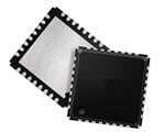
| 描述 | IC CPLD 128MC 7.24NS 32QFNFPGA - 现场可编程门阵列 256 LUTs 22 I/O 3.3V -4 Speed |
| 产品分类 | |
| I/O数 | 22 |
| 品牌 | Lattice Semiconductor Corporation |
| 产品手册 | |
| 产品图片 |
|
| rohs | 符合RoHS无铅 / 符合限制有害物质指令(RoHS)规范要求 |
| 产品系列 | 嵌入式处理器和控制器,FPGA - 现场可编程门阵列,Lattice LCMXO2-256HC-4SG32CMachXO2 |
| 数据手册 | |
| 产品型号 | LCMXO2-256HC-4SG32C |
| PCN组件/产地 | |
| PCN设计/规格 | |
| 产品 | MachXO2 |
| 产品种类 | FPGA - 现场可编程门阵列 |
| 供应商器件封装 | 32-QFNS(5x5) |
| 其它名称 | 220-2636 |
| 内嵌式块RAM-EBR | 0 bit |
| 分布式RAM | 2 kbit |
| 包装 | 托盘 |
| 可编程类型 | 系统内可编程 |
| 商标 | Lattice |
| 安装类型 | 表面贴装 |
| 安装风格 | SMD/SMT |
| 宏单元数 | 128 |
| 封装 | Tray |
| 封装/外壳 | 32-UFQFN 裸露焊盘 |
| 封装/箱体 | QFN-32 |
| 工作温度 | 0°C ~ 85°C |
| 工作电源电压 | 2.5 V, 3.3 V |
| 工作电源电流 | 18 uA |
| 工厂包装数量 | 490 |
| 延迟时间tpd(1)最大值 | 7.24ns |
| 总内存 | 2 kbit |
| 最大工作温度 | + 70 C |
| 最大工作频率 | 269 MHz |
| 最小工作温度 | 0 C |
| 栅极数 | - |
| 标准包装 | 490 |
| 电源电压-内部 | 2.375 V ~ 3.465 V |
| 系列 | LCMXO2-256HC-4SG |
| 输入/输出端数量 | 22 |
| 逻辑元件/块数 | 32 |
| 逻辑元件数量 | 256 |
| 逻辑数组块数量——LAB | 32 |


- 商务部:美国ITC正式对集成电路等产品启动337调查
- 曝三星4nm工艺存在良率问题 高通将骁龙8 Gen1或转产台积电
- 太阳诱电将投资9.5亿元在常州建新厂生产MLCC 预计2023年完工
- 英特尔发布欧洲新工厂建设计划 深化IDM 2.0 战略
- 台积电先进制程称霸业界 有大客户加持明年业绩稳了
- 达到5530亿美元!SIA预计今年全球半导体销售额将创下新高
- 英特尔拟将自动驾驶子公司Mobileye上市 估值或超500亿美元
- 三星加码芯片和SET,合并消费电子和移动部门,撤换高东真等 CEO
- 三星电子宣布重大人事变动 还合并消费电子和移动部门
- 海关总署:前11个月进口集成电路产品价值2.52万亿元 增长14.8%


PDF Datasheet 数据手册内容提取
MachXO2™ Family Data Sheet DS1035 Version 3.3, March 2017
MachXO2 Family Data Sheet Introduction May 2016 Data Sheet DS1035 Features Flexible On-Chip Clocking (cid:129) Eight primary clocks Flexible Logic Architecture (cid:129) Up to two edge clocks for high-speed I/O • Six devices with 256 to 6864 LUT4s and interfaces (top and bottom sides only) 18 to 334 I/Os (cid:129) Up to two analog PLLs per device with Ultra Low Power Devices fractional-n frequency synthesis (cid:129) Advanced 65 nm low power process – Wide input frequency range (7 MHz to (cid:129) As low as 22 µW standby power 400 MHz) (cid:129) Programmable low swing differential I/Os Non-volatile, Infinitely Reconfigurable (cid:129) Stand-by mode and other power saving options (cid:129) Instant-on – powers up in microseconds Embedded and Distributed Memory (cid:129) Single-chip, secure solution (cid:129) Up to 240 kbits sysMEM™ Embedded Block (cid:129) Programmable through JTAG, SPI or I2C RAM (cid:129) Supports background programming of non-vola- (cid:129) Up to 54 kbits Distributed RAM tile memory (cid:129) Dedicated FIFO control logic (cid:129) Optional dual boot with external SPI memory On-Chip User Flash Memory TransFR™ Reconfiguration (cid:129) Up to 256 kbits of User Flash Memory (cid:129) In-field logic update while system operates (cid:129) 100,000 write cycles Enhanced System Level Support (cid:129) Accessible through WISHBONE, SPI, I2C and (cid:129) On-chip hardened functions: SPI, I2C, timer/ JTAG interfaces counter (cid:129) Can be used as soft processor PROM or as (cid:129) On-chip oscillator with 5.5% accuracy Flash memory (cid:129) Unique TraceID for system tracking Pre-Engineered Source Synchronous I/O (cid:129) One Time Programmable (OTP) mode (cid:129) DDR registers in I/O cells (cid:129) Single power supply with extended operating (cid:129) Dedicated gearing logic range (cid:129) 7:1 Gearing for Display I/Os (cid:129) IEEE Standard 1149.1 boundary scan (cid:129) Generic DDR, DDRX2, DDRX4 (cid:129) IEEE 1532 compliant in-system programming (cid:129) Dedicated DDR/DDR2/LPDDR memory with Broad Range of Package Options DQS support (cid:129) TQFP, WLCSP, ucBGA, csBGA, caBGA, ftBGA, High Performance, Flexible I/O Buffer fpBGA, QFN package options (cid:129) Programmable sysIO™ buffer supports wide (cid:129) Small footprint package options range of interfaces: – As small as 2.5 mm x 2.5 mm – LVCMOS 3.3/2.5/1.8/1.5/1.2 (cid:129) Density migration supported – LVTTL (cid:129) Advanced halogen-free packaging – PCI – LVDS, Bus-LVDS, MLVDS, RSDS, LVPECL – SSTL 25/18 – HSTL 18 – Schmitt trigger inputs, up to 0.5 V hysteresis (cid:129) I/Os support hot socketing (cid:129) On-chip differential termination (cid:129) Programmable pull-up or pull-down mode © 2016 Lattice Semiconductor Corp. All Lattice trademarks, registered trademarks, patents, and disclaimers are as listed at www.latticesemi.com/legal. All other brand or product names are trademarks or registered trademarks of their respective holders. The specifications and information herein are subject to change without notice. www.latticesemi.com 1-1 DS1035 Introduction_02.2
Introduction MachXO2 Family Data Sheet Table 1-1. MachXO2™ Family Selection Guide XO2-256 XO2-640 XO2-640U1 XO2-1200 XO2-1200U1 XO2-2000 XO2-2000U1 XO2-4000 XO2-7000 LUTs 256 640 640 1280 1280 2112 2112 4320 6864 Distributed RAM (kbits) 2 5 5 10 10 16 16 34 54 EBR SRAM (kbits) 0 18 64 64 74 74 92 92 240 Number of EBR SRAM Blocks (9 0 2 7 7 8 8 10 10 26 kbits/block) UFM (kbits) 0 24 64 64 80 80 96 96 256 Device Options: HC2 Yes Yes Yes Yes Yes Yes Yes Yes Yes HE3 Yes Yes Yes Yes ZE4 Yes Yes Yes Yes Yes Yes Number of PLLs 0 0 1 1 1 1 2 2 2 Hardened I2C 2 2 2 2 2 2 2 2 2 Functions: SPI 1 1 1 1 1 1 1 1 1 Timer/Coun- 1 1 1 1 1 1 1 1 1 ter Packages IO 25-ball WLCSP5 18 (2.5 mm x 2.5 mm, 0.4 mm) 32 QFN6 21 21 (5 mm x 5 mm, 0.5 mm) 48 QFN8, 9 40 40 (7 mm x 7 mm, 0.5 mm) 49-ball WLCSP5 38 (3.2 mm x 3.2 mm, 0.4 mm) 64-ball ucBGA 44 (4 mm x 4 mm, 0.4 mm) 84 QFN7 68 (7 mm x 7 mm, 0.5 mm) 100-pin TQFP 55 78 79 79 (14 mm x 14 mm) 132-ball csBGA 55 79 104 104 104 (8 mm x 8 mm, 0.5 mm) 144-pin TQFP 107 107 111 114 114 (20 mm x 20 mm) 184-ball csBGA7 150 (8 mm x 8 mm, 0.5 mm) 256-ball caBGA 206 206 206 (14 mm x 14 mm, 0.8 mm) 256-ball ftBGA 206 206 206 206 (17 mm x 17 mm, 1.0 mm) 332-ball caBGA 274 278 (17 mm x 17 mm, 0.8 mm) 484-ball ftBGA 278 278 334 (23 mm x 23 mm, 1.0 mm) 1. Ultra high I/O device. 2. High performance with regulator – VCC = 2.5 V, 3.3 V 3. High performance without regulator – V = 1.2 V CC 4. Low power without regulator – V = 1.2 V CC 5. WLCSP package only available for ZE devices. 6. 32 QFN package only available for HC and ZE devices. 7. 184 csBGA package only available for HE devices. 8. 48-pin QFN information is ‘Advanced’. 9. 48 QFN package only available for HC devices. 1-2
Introduction MachXO2 Family Data Sheet Introduction The MachXO2 family of ultra low power, instant-on, non-volatile PLDs has six devices with densities ranging from 256 to 6864 Look-Up Tables (LUTs). In addition to LUT-based, low-cost programmable logic these devices feature Embedded Block RAM (EBR), Distributed RAM, User Flash Memory (UFM), Phase Locked Loops (PLLs), pre- engineered source synchronous I/O support, advanced configuration support including dual-boot capability and hardened versions of commonly used functions such as SPI controller, I2C controller and timer/counter. These fea- tures allow these devices to be used in low cost, high volume consumer and system applications. The MachXO2 devices are designed on a 65 nm non-volatile low power process. The device architecture has sev- eral features such as programmable low swing differential I/Os and the ability to turn off I/O banks, on-chip PLLs and oscillators dynamically. These features help manage static and dynamic power consumption resulting in low static power for all members of the family. The MachXO2 devices are available in two versions – ultra low power (ZE) and high performance (HC and HE) devices. The ultra low power devices are offered in three speed grades –1, –2 and –3, with –3 being the fastest. Similarly, the high-performance devices are offered in three speed grades: –4, –5 and –6, with –6 being the fastest. HC devices have an internal linear voltage regulator which supports external V supply voltages of 3.3 V or 2.5 V. CC ZE and HE devices only accept 1.2 V as the external V supply voltage. With the exception of power supply volt- CC age all three types of devices (ZE, HC and HE) are functionally compatible and pin compatible with each other. The MachXO2 PLDs are available in a broad range of advanced halogen-free packages ranging from the space saving 2.5 mm x 2.5 mm WLCSP to the 23 mm x 23 mm fpBGA. MachXO2 devices support density migration within the same package. Table 1-1 shows the LUT densities, package and I/O options, along with other key parameters. The pre-engineered source synchronous logic implemented in the MachXO2 device family supports a broad range of interface standards, including LPDDR, DDR, DDR2 and 7:1 gearing for display I/Os. The MachXO2 devices offer enhanced I/O features such as drive strength control, slew rate control, PCI compati- bility, bus-keeper latches, pull-up resistors, pull-down resistors, open drain outputs and hot socketing. Pull-up, pull- down and bus-keeper features are controllable on a “per-pin” basis. A user-programmable internal oscillator is included in MachXO2 devices. The clock output from this oscillator may be divided by the timer/counter for use as clock input in functions such as LED control, key-board scanner and sim- ilar state machines. The MachXO2 devices also provide flexible, reliable and secure configuration from on-chip Flash memory. These devices can also configure themselves from external SPI Flash or be configured by an external master through the JTAG test access port or through the I2C port. Additionally, MachXO2 devices support dual-boot capability (using external Flash memory) and remote field upgrade (TransFR) capability. Lattice provides a variety of design tools that allow complex designs to be efficiently implemented using the MachXO2 family of devices. Popular logic synthesis tools provide synthesis library support for MachXO2. Lattice design tools use the synthesis tool output along with the user-specified preferences and constraints to place and route the design in the MachXO2 device. These tools extract the timing from the routing and back-annotate it into the design for timing verification. Lattice provides many pre-engineered IP (Intellectual Property) LatticeCORE™ modules, including a number of reference designs licensed free of charge, optimized for the MachXO2 PLD family. By using these configurable soft core IP cores as standardized blocks, users are free to concentrate on the unique aspects of their design, increas- ing their productivity. 1-3
MachXO2 Family Data Sheet Architecture March 2016 Data Sheet DS1035 Architecture Overview The MachXO2 family architecture contains an array of logic blocks surrounded by Programmable I/O (PIO). The larger logic density devices in this family have sysCLOCK™ PLLs and blocks of sysMEM Embedded Block RAM (EBRs). Figure 2-1 and Figure 2-2 show the block diagrams of the various family members. Figure 2-1. Top View of the MachXO2-1200 Device Embedded Function Block (EFB) User Flash Memory (UFM) sysCLOCK PLL sysMEM Embedded Block RAM (EBR) On-chip Configuration Flash Memory Programmable Function Units with Distributed RAM (PFUs) PIOs Arranged into sysIO Banks Note: MachXO2-256, and MachXO2-640/U are similar to MachXO2-1200. MachXO2-256 has a lower LUT count and no PLL or EBR blocks. MachXO2-640 has no PLL, a lower LUT count and two EBR blocks. MachXO2-640U has a lower LUT count, one PLL and seven EBR blocks. Figure 2-2. Top View of the MachXO2-4000 Device Embedded Function Block(EFB) User Flash Memory (UFM) sysCLOCK PLL On-chip Configuration Flash Memory sysMEM Embedded PIOs Arranged into Block RAM (EBR) sysIO Banks Programmable Function Units with Distributed RAM (PFUs) Note: MachXO2-1200U, MachXO2-2000/U and MachXO2-7000 are similar to MachXO2-4000. MachXO2-1200U and MachXO2-2000 have a lower LUT count, one PLL, and eight EBR blocks. MachXO2-2000U has a lower LUT count, two PLLs, and 10 EBR blocks. MachXO2-7000 has a higher LUT count, two PLLs, and 26 EBR blocks. © 2016 Lattice Semiconductor Corp. All Lattice trademarks, registered trademarks, patents, and disclaimers are as listed at www.latticesemi.com/legal. All other brand or product names are trademarks or registered trademarks of their respective holders. The specifications and information herein are subject to change without notice. www.latticesemi.com 2-1 DS1035 Architecture_02.3
Architecture MachXO2 Family Data Sheet The logic blocks, Programmable Functional Unit (PFU) and sysMEM EBR blocks, are arranged in a two-dimen- sional grid with rows and columns. Each row has either the logic blocks or the EBR blocks. The PIO cells are located at the periphery of the device, arranged in banks. The PFU contains the building blocks for logic, arithmetic, RAM, ROM, and register functions. The PIOs utilize a flexible I/O buffer referred to as a sysIO buffer that supports operation with a variety of interface standards. The blocks are connected with many vertical and horizontal routing channel resources. The place and route software tool automatically allocates these routing resources. In the MachXO2 family, the number of sysIO banks varies by device. There are different types of I/O buffers on the different banks. Refer to the details in later sections of this document. The sysMEM EBRs are large, dedicated fast memory blocks; these blocks are found in MachXO2-640/U and larger devices. These blocks can be configured as RAM, ROM or FIFO. FIFO support includes dedicated FIFO pointer and flag “hard” control logic to minimize LUT usage. The MachXO2 registers in PFU and sysI/O can be configured to be SET or RESET. After power up and device is configured, the device enters into user mode with these registers SET/RESET according to the configuration set- ting, allowing device entering to a known state for predictable system function. The MachXO2 architecture also provides up to two sysCLOCK Phase Locked Loop (PLL) blocks on MachXO2- 640U, MachXO2-1200/U and larger devices. These blocks are located at the ends of the on-chip Flash block. The PLLs have multiply, divide, and phase shifting capabilities that are used to manage the frequency and phase rela- tionships of the clocks. MachXO2 devices provide commonly used hardened functions such as SPI controller, I2C controller and timer/ counter. MachXO2-640/U and higher density devices also provide User Flash Memory (UFM). These hardened functions and the UFM interface to the core logic and routing through a WISHBONE interface. The UFM can also be accessed through the SPI, I2C and JTAG ports. Every device in the family has a JTAG port that supports programming and configuration of the device as well as access to the user logic. The MachXO2 devices are available for operation from 3.3 V, 2.5 V and 1.2 V power sup- plies, providing easy integration into the overall system. PFU Blocks The core of the MachXO2 device consists of PFU blocks, which can be programmed to perform logic, arithmetic, distributed RAM and distributed ROM functions. Each PFU block consists of four interconnected slices numbered 0 to 3 as shown in Figure 2-3. Each slice contains two LUTs and two registers. There are 53 inputs and 25 outputs associated with each PFU block. 2-2
Architecture MachXO2 Family Data Sheet Figure 2-3. PFU Block Diagram From Routin g LUT4 & LUT4 & LUT4 & LUT4 & LUT4 & LUT4 & LUT4 & LUT4 & FCIN CARRY CARRY CARRY CARRY CARRY CARRY CARRY CARRY FCO Slice 0 Slice 1 Slice 2 Slice 3 D D D D D D D D FF/ FF/ FF/ FF/ FF/ FF/ FF/ FF/ Latch Latch Latch Latch Latch Latch Latch Latch To Routin g Slices Slices 0-3 contain two LUT4s feeding two registers. Slices 0-2 can be configured as distributed memory. Table 2-1 shows the capability of the slices in PFU blocks along with the operation modes they enable. In addition, each PFU contains logic that allows the LUTs to be combined to perform functions such as LUT5, LUT6, LUT7 and LUT8. The control logic performs set/reset functions (programmable as synchronous/ asynchronous), clock select, chip- select and wider RAM/ROM functions. Table 2-1. Resources and Modes Available per Slice PFU Block Slice Resources Modes Slice 0 2 LUT4s and 2 Registers Logic, Ripple, RAM, ROM Slice 1 2 LUT4s and 2 Registers Logic, Ripple, RAM, ROM Slice 2 2 LUT4s and 2 Registers Logic, Ripple, RAM, ROM Slice 3 2 LUT4s and 2 Registers Logic, Ripple, ROM Figure 2-4 shows an overview of the internal logic of the slice. The registers in the slice can be configured for posi- tive/negative and edge triggered or level sensitive clocks. All slices have 15 inputs from routing and one from the carry-chain (from the adjacent slice or PFU). There are seven outputs: six for routing and one to carry-chain (to the adjacent PFU). Table 2-2 lists the signals associated with Slices 0-3. 2-3
Architecture MachXO2 Family Data Sheet Figure 2-4. Slice Diagram FCO To Different Slice/PFU Slice FXB OFX1 FXA A1 CO F1 B1 F/SUM C1 D1 LUT4 & D Q1 Carry Flip-flop/ Latch CI To Routing M1 M0 LUT5 From Mux Routing OFX0 A0 CO B0 C0 F0 D0 LUT4 & Carry F/SUM D Q0 Flip-flop/ CI Latch CE CLK LSR Memory & FCI From Control Different Signals Slice/PFU For Slices 0 and 1, memory control signals are generated from Slice 2 as follows: • WCK is CLK • WRE is from LSR • DI[3:2] for Slice 1 and DI[1:0] for Slice 0 data from Slice 2 • WAD [A:D] is a 4-bit address from slice 2 LUT input Table 2-2. Slice Signal Descriptions Function Type Signal Names Description Input Data signal A0, B0, C0, D0 Inputs to LUT4 Input Data signal A1, B1, C1, D1 Inputs to LUT4 Input Multi-purpose M0/M1 Multi-purpose input Input Control signal CE Clock enable Input Control signal LSR Local set/reset Input Control signal CLK System clock Input Inter-PFU signal FCIN Fast carry in1 Output Data signals F0, F1 LUT4 output register bypass signals Output Data signals Q0, Q1 Register outputs Output Data signals OFX0 Output of a LUT5 MUX Output Data signals OFX1 Output of a LUT6, LUT7, LUT82 MUX depending on the slice Output Inter-PFU signal FCO Fast carry out1 1. See Figure 2-3 for connection details. 2. Requires two PFUs. 2-4
Architecture MachXO2 Family Data Sheet Modes of Operation Each slice has up to four potential modes of operation: Logic, Ripple, RAM and ROM. Logic Mode In this mode, the LUTs in each slice are configured as 4-input combinatorial lookup tables. A LUT4 can have 16 possible input combinations. Any four input logic functions can be generated by programming this lookup table. Since there are two LUT4s per slice, a LUT5 can be constructed within one slice. Larger look-up tables such as LUT6, LUT7 and LUT8 can be constructed by concatenating other slices. Note LUT8 requires more than four slices. Ripple Mode Ripple mode supports the efficient implementation of small arithmetic functions. In Ripple mode, the following func- tions can be implemented by each slice: (cid:129) Addition 2-bit (cid:129) Subtraction 2-bit (cid:129) Add/subtract 2-bit using dynamic control (cid:129) Up counter 2-bit (cid:129) Down counter 2-bit (cid:129) Up/down counter with asynchronous clear (cid:129) Up/down counter with preload (sync) (cid:129) Ripple mode multiplier building block (cid:129) Multiplier support (cid:129) Comparator functions of A and B inputs — A greater-than-or-equal-to B — A not-equal-to B — A less-than-or-equal-to B Ripple mode includes an optional configuration that performs arithmetic using fast carry chain methods. In this con- figuration (also referred to as CCU2 mode) two additional signals, Carry Generate and Carry Propagate, are gener- ated on a per-slice basis to allow fast arithmetic functions to be constructed by concatenating slices. RAM Mode In this mode, a 16x4-bit distributed single port RAM (SPR) can be constructed by using each LUT block in Slice 0 and Slice 1 as a 16x1-bit memory. Slice 2 is used to provide memory address and control signals. MachXO2 devices support distributed memory initialization. The Lattice design tools support the creation of a variety of different size memories. Where appropriate, the soft- ware will construct these using distributed memory primitives that represent the capabilities of the PFU. Table 2-3 shows the number of slices required to implement different distributed RAM primitives. For more information about using RAM in MachXO2 devices, please see TN1201, Memory Usage Guide for MachXO2 Devices. Table 2-3. Number of Slices Required For Implementing Distributed RAM SPR 16x4 PDPR 16x4 Number of slices 3 3 Note: SPR = Single Port RAM, PDPR = Pseudo Dual Port RAM 2-5
Architecture MachXO2 Family Data Sheet ROM Mode ROM mode uses the LUT logic; hence, slices 0-3 can be used in ROM mode. Preloading is accomplished through the programming interface during PFU configuration. For more information on the RAM and ROM modes, please refer to TN1201, Memory Usage Guide for MachXO2 Devices. Routing There are many resources provided in the MachXO2 devices to route signals individually or as buses with related control signals. The routing resources consist of switching circuitry, buffers and metal interconnect (routing) seg- ments. The inter-PFU connections are made with three different types of routing resources: x1 (spans two PFUs), x2 (spans three PFUs) and x6 (spans seven PFUs). The x1, x2, and x6 connections provide fast and efficient connec- tions in the horizontal and vertical directions. The design tools take the output of the synthesis tool and places and routes the design. Generally, the place and route tool is completely automatic, although an interactive routing editor is available to optimize the design. Clock/Control Distribution Network Each MachXO2 device has eight clock inputs (PCLK [T, C] [Banknum]_[2..0]) – three pins on the left side, two pins each on the bottom and top sides and one pin on the right side. These clock inputs drive the clock nets. These eight inputs can be differential or single-ended and may be used as general purpose I/O if they are not used to drive the clock nets. When using a single ended clock input, only the PCLKT input can drive the clock tree directly. The MachXO2 architecture has three types of clocking resources: edge clocks, primary clocks and secondary high fanout nets. MachXO2-640U, MachXO2-1200/U and higher density devices have two edge clocks each on the top and bottom edges. Lower density devices have no edge clocks. Edge clocks are used to clock I/O registers and have low injection time and skew. Edge clock inputs are from PLL outputs, primary clock pads, edge clock bridge outputs and CIB sources. The eight primary clock lines in the primary clock network drive throughout the entire device and can provide clocks for all resources within the device including PFUs, EBRs and PICs. In addition to the primary clock signals, MachXO2 devices also have eight secondary high fanout signals which can be used for global control signals, such as clock enables, synchronous or asynchronous clears, presets, output enables, etc. Internal logic can drive the global clock network for internally-generated global clocks and control signals. The maximum frequency for the primary clock network is shown in the MachXO2 External Switching Characteris- tics table. The primary clock signals for the MachXO2-256 and MachXO2-640 are generated from eight 17:1 muxes The available clock sources include eight I/O sources and 9 routing inputs. Primary clock signals for the MachXO2- 640U, MachXO2-1200/U and larger devices are generated from eight 27:1 muxes The available clock sources include eight I/O sources, 11 routing inputs, eight clock divider inputs and up to eight sysCLOCK PLL outputs. 2-6
Architecture MachXO2 Family Data Sheet Figure 2-5. Primary Clocks for MachXO2 Devices Up to 8 8 11 8 Dynamic 27:1 Clock Primary Clock 0 Enable Dynamic 27:1 Clock Primary Clock 1 Enable Dynamic 27:1 Clock Primary Clock 2 Enable Dynamic 27:1 Clock Primary Clock 3 Enable Dynamic 27:1 Clock Primary Clock 4 Enable Dynamic 27:1 Clock Primary Clock 5 Enable 27:1 Dynamic Clock Enable Primary Clock 6 27:1 Clock Switch 27:1 Dynamic Clock Enable Primary Clock 7 27:1 Clock PLL Outputs Clock Pads Routing Edge Clock Divider Switch Primary clocks for MachXO2-640U, MachXO2-1200/U and larger devices. Note: MachXO2-640 and smaller devices do not have inputs from the Edge Clock Divider or PLL and fewer routing inputs. These devices have 17:1 muxes instead of 27:1 muxes. Eight secondary high fanout nets are generated from eight 8:1 muxes as shown in Figure 2-6. One of the eight inputs to the secondary high fanout net input mux comes from dual function clock pins and the remaining seven come from internal routing. The maximum frequency for the secondary clock network is shown in MachXO2 Exter- nal Switching Characteristics table. 2-7
Architecture MachXO2 Family Data Sheet Figure 2-6. Secondary High Fanout Nets for MachXO2 Devices 1 7 Secondary High 8:1 Fanout Net 0 Secondary High 8:1 Fanout Net 1 Secondary High 8:1 Fanout Net 2 Secondary High 8:1 Fanout Net 3 Secondary High 8:1 Fanout Net 4 Secondary High 8:1 Fanout Net 5 Secondary High 8:1 Fanout Net 6 Secondary High 8:1 Fanout Net 7 Clock Pads Routing sysCLOCK Phase Locked Loops (PLLs) The sysCLOCK PLLs provide the ability to synthesize clock frequencies. The MachXO2-640U, MachXO2-1200/U and larger devices have one or more sysCLOCK PLL. CLKI is the reference frequency input to the PLL and its source can come from an external I/O pin or from internal routing. CLKFB is the feedback signal to the PLL which can come from internal routing or an external I/O pin. The feedback divider is used to multiply the reference fre- quency and thus synthesize a higher frequency clock output. The MachXO2 sysCLOCK PLLs support high resolution (16-bit) fractional-N synthesis. Fractional-N frequency syn- thesis allows the user to generate an output clock which is a non-integer multiple of the input frequency. For more information about using the PLL with Fractional-N synthesis, please see TN1199, MachXO2 sysCLOCK PLL Design and Usage Guide. Each output has its own output divider, thus allowing the PLL to generate different frequencies for each output. The output dividers can have a value from 1 to 128. The output dividers may also be cascaded together to generate low frequency clocks. The CLKOP, CLKOS, CLKOS2, and CLKOS3 outputs can all be used to drive the MachXO2 clock distribution network directly or general purpose routing resources can be used. The LOCK signal is asserted when the PLL determines it has achieved lock and de-asserted if a loss of lock is detected. A block diagram of the PLL is shown in Figure 2-7. The setup and hold times of the device can be improved by programming a phase shift into the CLKOS, CLKOS2, and CLKOS3 output clocks which will advance or delay the output clock with reference to the CLKOP output clock. 2-8
Architecture MachXO2 Family Data Sheet This phase shift can be either programmed during configuration or can be adjusted dynamically. In dynamic mode, the PLL may lose lock after a phase adjustment on the output used as the feedback source and not relock until the t parameter has been satisfied. LOCK The MachXO2 also has a feature that allows the user to select between two different reference clock sources dynamically. This feature is implemented using the PLLREFCS primitive. The timing parameters for the PLL are shown in the sysCLOCK PLL Timing table. The MachXO2 PLL contains a WISHBONE port feature that allows the PLL settings, including divider values, to be dynamically changed from the user logic. When using this feature the EFB block must also be instantiated in the design to allow access to the WISHBONE ports. Similar to the dynamic phase adjustment, when PLL settings are updated through the WISHBONE port the PLL may lose lock and not relock until the t parameter has been sat- LOCK isfied. The timing parameters for the PLL are shown in the sysCLOCK PLL Timing table. For more details on the PLL and the WISHBONE interface, see TN1199, MachXO2 sysCLOCK PLL Design and Usage Guide. Figure 2-7. PLL Diagram DPHSRC PHASESEL[1:0] Dynamic PHASEDIR Phase PHASESTEP Adjust CLKOP CLKOP Phase A2 ClkEn A0 Divider Adjust/ STDBY Mux Synch (1 - 128) Edge Trim REFCLK CLKOS CLKI REFCLK B0 B1 CDLivKidOeSr APdhjausset/ B2 ClkEn Divider Phase detector, Mux (1 - 128) Edge Trim Mux Synch M (1 - 40) VCO, and loop filter. CLKFB FBKSEL CLKOS2 CLKOS2 C1 Phase C2 ClkEn FBKCLK Fractional-N C0 Mux Divider Adjust Mux Synch Divider Synthesizer (1 - 128) N (1 - 40) CLKOS3 CLKOS3 D1 Phase D2 ClkEn D0 Divider Mux Adjust Mux Synch Internal Feedback (1 - 128) CLKOP, CLKOS, CLKOS2, CLKOS3 LOCK Lock 4 RST, RESETM, RESETC, RESETD Detect ENCLKOP, ENCLKOS, ENCLKOS2, ENCLKOS3 PLLDATO[7:0] , PLLACK PLLCLK, PLLRST, PLLSTB, PLLWE, PLLDATI[7:0], PLLADDR[4:0] Table 2-4 provides signal descriptions of the PLL block. Table 2-4. PLL Signal Descriptions Port Name I/O Description CLKI I Input clock to PLL CLKFB I Feedback clock PHASESEL[1:0] I Select which output is affected by Dynamic Phase adjustment ports PHASEDIR I Dynamic Phase adjustment direction PHASESTEP I Dynamic Phase step – toggle shifts VCO phase adjust by one step. 2-9
Architecture MachXO2 Family Data Sheet Table 2-4. PLL Signal Descriptions (Continued) Port Name I/O Description CLKOP O Primary PLL output clock (with phase shift adjustment) CLKOS O Secondary PLL output clock (with phase shift adjust) CLKOS2 O Secondary PLL output clock2 (with phase shift adjust) CLKOS3 O Secondary PLL output clock3 (with phase shift adjust) PLL LOCK, asynchronous signal. Active high indicates PLL is locked to input and feed- LOCK O back signals. DPHSRC O Dynamic Phase source – ports or WISHBONE is active STDBY I Standby signal to power down the PLL RST I PLL reset without resetting the M-divider. Active high reset. RESETM I PLL reset - includes resetting the M-divider. Active high reset. RESETC I Reset for CLKOS2 output divider only. Active high reset. RESETD I Reset for CLKOS3 output divider only. Active high reset. ENCLKOP I Enable PLL output CLKOP ENCLKOS I Enable PLL output CLKOS when port is active ENCLKOS2 I Enable PLL output CLKOS2 when port is active ENCLKOS3 I Enable PLL output CLKOS3 when port is active PLLCLK I PLL data bus clock input signal PLLRST I PLL data bus reset. This resets only the data bus not any register values. PLLSTB I PLL data bus strobe signal PLLWE I PLL data bus write enable signal PLLADDR [4:0] I PLL data bus address PLLDATI [7:0] I PLL data bus data input PLLDATO [7:0] O PLL data bus data output PLLACK O PLL data bus acknowledge signal sysMEM Embedded Block RAM Memory The MachXO2-640/U and larger devices contain sysMEM Embedded Block RAMs (EBRs). The EBR consists of a 9-kbit RAM, with dedicated input and output registers. This memory can be used for a wide variety of purposes including data buffering, PROM for the soft processor and FIFO. sysMEM Memory Block The sysMEM block can implement single port, dual port, pseudo dual port, or FIFO memories. Each block can be used in a variety of depths and widths as shown in Table 2-5. 2-10
Architecture MachXO2 Family Data Sheet Table 2-5. sysMEM Block Configurations Memory Mode Configurations 8,192 x 1 4,096 x 2 Single Port 2,048 x 4 1,024 x 9 8,192 x 1 4,096 x 2 True Dual Port 2,048 x 4 1,024 x 9 8,192 x 1 4,096 x 2 Pseudo Dual Port 2,048 x 4 1,024 x 9 512 x 18 8,192 x 1 4,096 x 2 FIFO 2,048 x 4 1,024 x 9 512 x 18 Bus Size Matching All of the multi-port memory modes support different widths on each of the ports. The RAM bits are mapped LSB word 0 to MSB word 0, LSB word 1 to MSB word 1, and so on. Although the word size and number of words for each port varies, this mapping scheme applies to each port. RAM Initialization and ROM Operation If desired, the contents of the RAM can be pre-loaded during device configuration. EBR initialization data can be loaded from the UFM. To maximize the number of UFM bits, initialize the EBRs used in your design to an all-zero pattern. Initializing to an all-zero pattern does not use up UFM bits. MachXO2 devices have been designed such that multiple EBRs share the same initialization memory space if they are initialized to the same pattern. By preloading the RAM block during the chip configuration cycle and disabling the write controls, the sysMEM block can also be utilized as a ROM. Memory Cascading Larger and deeper blocks of RAM can be created using EBR sysMEM Blocks. Typically, the Lattice design tools cascade memory transparently, based on specific design inputs. Single, Dual, Pseudo-Dual Port and FIFO Modes Figure 2-8 shows the five basic memory configurations and their input/output names. In all the sysMEM RAM modes, the input data and addresses for the ports are registered at the input of the memory array. The output data of the memory is optionally registered at the memory array output. 2-11
Architecture MachXO2 Family Data Sheet Figure 2-8. sysMEM Memory Primitives AD[12:0] DIA[8:0] DI[8:0] DI[8:0] ADW[8:0] ADA[12:0] ADB[12:0] DI[17:0] ADR[12:0] CLK CLKA CLKB BE[1:0] CLKR CE CEA CEB CLKW OCE CER EBR DO[8:0] RSTA EBR RSTB CEW EBR RST WEA WEB RST DO[17:0] WE CSA[2:0] CSB[2:0] OCER CS[2:0] OCEA OCEB CSW[2:0] CSR[2:0] DOA[8:0] DOB[8:0] Single-Port RAM True Dual Port RAM Pseudo Dual Port RAM AD[12:0] AFF DI[17:0] FF AEF CLKW EF CLK WE DO[17:0] CE EBR ORE OCE EBR DO[17:0] RST CLKR FULLI RE RST CSW[1:0] EMPTYI CSR[1:0] CS[2:0] RPRST FIFO RAM ROM Table 2-6. EBR Signal Descriptions Port Name Description Active State CLK Clock Rising Clock Edge CE Clock Enable Active High OCE1 Output Clock Enable Active High RST Reset Active High BE1 Byte Enable Active High WE Write Enable Active High AD Address Bus — DI Data In — DO Data Out — CS Chip Select Active High AFF FIFO RAM Almost Full Flag — FF FIFO RAM Full Flag — AEF FIFO RAM Almost Empty Flag — EF FIFO RAM Empty Flag — RPRST FIFO RAM Read Pointer Reset — 1. Optional signals. 2. For dual port EBR primitives a trailing ‘A’ or ‘B’ in the signal name specifies the EBR port A or port B respectively. 3. For FIFO RAM mode primitive, a trailing ‘R’ or ‘W’ in the signal name specifies the FIFO read port or write port respec- tively. 4. For FIFO RAM mode primitive FULLI has the same function as CSW(2) and EMPTYI has the same function as CSR(2). 5. In FIFO mode, CLKW is the write port clock, CSW is the write port chip select, CLKR is the read port clock, CSR is the read port chip select, ORE is the output read enable. 2-12
Architecture MachXO2 Family Data Sheet The EBR memory supports three forms of write behavior for single or dual port operation: 1. Normal – Data on the output appears only during the read cycle. During a write cycle, the data (at the current address) does not appear on the output. This mode is supported for all data widths. 2. Write Through – A copy of the input data appears at the output of the same port. This mode is supported for all data widths. 3. Read-Before-Write – When new data is being written, the old contents of the address appears at the output. FIFO Configuration The FIFO has a write port with data-in, CEW, WE and CLKW signals. There is a separate read port with data-out, RCE, RE and CLKR signals. The FIFO internally generates Almost Full, Full, Almost Empty and Empty Flags. The Full and Almost Full flags are registered with CLKW. The Empty and Almost Empty flags are registered with CLKR. Table 2-7 shows the range of programming values for these flags. Table 2-7. Programmable FIFO Flag Ranges Flag Name Programming Range Full (FF) 1 to max (up to 2N-1) Almost Full (AF) 1 to Full-1 Almost Empty (AE) 1 to Full-1 Empty (EF) 0 N = Address bit width. The FIFO state machine supports two types of reset signals: RST and RPRST. The RST signal is a global reset that clears the contents of the FIFO by resetting the read/write pointer and puts the FIFO flags in their initial reset state. The RPRST signal is used to reset the read pointer. The purpose of this reset is to retransmit the data that is in the FIFO. In these applications it is important to keep careful track of when a packet is written into or read from the FIFO. Memory Core Reset The memory core contains data output latches for ports A and B. These are simple latches that can be reset syn- chronously or asynchronously. RSTA and RSTB are local signals, which reset the output latches associated with port A and port B respectively. The Global Reset (GSRN) signal resets both ports. The output data latches and associated resets for both ports are as shown in Figure 2-9. 2-13
Architecture MachXO2 Family Data Sheet Figure 2-9. Memory Core Reset Memory Core DSETQ Port A[18:0] Output Data Latches DSETQ Port B[18:0] RSTA RSTB GSRN Programmable Disable For further information on the sysMEM EBR block, please refer to TN1201, Memory Usage Guide for MachXO2 Devices. EBR Asynchronous Reset EBR asynchronous reset or GSR (if used) can only be applied if all clock enables are low for a clock cycle before the reset is applied and released a clock cycle after the reset is released, as shown in Figure 2-10. The GSR input to the EBR is always asynchronous. Figure 2-10. EBR Asynchronous Reset (Including GSR) Timing Diagram Reset Clock Clock Enable If all clock enables remain enabled, the EBR asynchronous reset or GSR may only be applied and released after the EBR read and write clock inputs are in a steady state condition for a minimum of 1/f (EBR clock). The reset MAX release must adhere to the EBR synchronous reset setup time before the next active read or write clock edge. If an EBR is pre-loaded during configuration, the GSR input must be disabled or the release of the GSR during device wake up must occur before the release of the device I/Os becoming active. These instructions apply to all EBR RAM, ROM and FIFO implementations. For the EBR FIFO mode, the GSR sig- nal is always enabled and the WE and RE signals act like the clock enable signals in Figure 2-10. The reset timing rules apply to the RPReset input versus the RE input and the RST input versus the WE and RE inputs. Both RST and RPReset are always asynchronous EBR inputs. For more details refer to TN1201, Memory Usage Guide for MachXO2 Devices. Note that there are no reset restrictions if the EBR synchronous reset is used and the EBR GSR input is disabled. 2-14
Architecture MachXO2 Family Data Sheet Programmable I/O Cells (PIC) The programmable logic associated with an I/O is called a PIO. The individual PIO are connected to their respec- tive sysIO buffers and pads. On the MachXO2 devices, the PIO cells are assembled into groups of four PIO cells called a Programmable I/O Cell or PIC. The PICs are placed on all four sides of the device. On all the MachXO2 devices, two adjacent PIOs can be combined to provide a complementary output driver pair. The MachXO2-640U, MachXO2-1200/U and higher density devices contain enhanced I/O capability. All PIO pairs on these larger devices can implement differential receivers. Half of the PIO pairs on the top edge of these devices can be configured as true LVDS transmit pairs. The PIO pairs on the bottom edge of these higher density devices have on-chip differential termination and also provide PCI support. 2-15
Architecture MachXO2 Family Data Sheet Figure 2-11. Group of Four Programmable I/O Cells 1 PIC PIO A Input Register Block Output Register Block Pin & Tristate A Register Block PIO B Input Register Block Output Register Block Pin & Tristate B Register Block Core Logic/ Input Output Routing Gearbox Gearbox PIO C Input Register Block Output Register Block Pin & Tristate C Register Block PIO D Input Register Block Output Register Block Pin & Tristate D Register Block Notes: 1. Input gearbox is available only in PIC on the bottom edge of MachXO2-640U, MachXO2-1200/U and larger devices. 2. Output gearbox is available only in PIC on the top edge of MachXO2-640U, MachXO2-1200/U and larger devices. 2-16
Architecture MachXO2 Family Data Sheet PIO The PIO contains three blocks: an input register block, output register block and tri-state register block. These blocks contain registers for operating in a variety of modes along with the necessary clock and selection logic. Table 2-8. PIO Signal List Pin Name I/O Type Description CE Input Clock Enable D Input Pin input from sysIO buffer. INDD Output Register bypassed input. INCK Output Clock input Q0 Output DDR positive edge input Q1 Output Registered input/DDR negative edge input D0 Input Output signal from the core (SDR and DDR) D1 Input Output signal from the core (DDR) TD Input Tri-state signal from the core Q Output Data output signals to sysIO Buffer TQ Output Tri-state output signals to sysIO Buffer DQSR901 Input DQS shift 90-degree read clock DQSW901 Input DQS shift 90-degree write clock DDRCLKPOL1 Input DDR input register polarity control signal from DQS SCLK Input System clock for input and output/tri-state blocks. RST Input Local set reset signal 1. Available in PIO on right edge only. Input Register Block The input register blocks for the PIOs on all edges contain delay elements and registers that can be used to condi- tion high-speed interface signals before they are passed to the device core. In addition to this functionality, the input register blocks for the PIOs on the right edge include built-in logic to interface to DDR memory. Figure 2-12 shows the input register block for the PIOs located on the left, top and bottom edges. Figure 2-13 shows the input register block for the PIOs on the right edge. Left, Top, Bottom Edges Input signals are fed from the sysIO buffer to the input register block (as signal D). If desired, the input signal can bypass the register and delay elements and be used directly as a combinatorial signal (INDD), and a clock (INCK). If an input delay is desired, users can select a fixed delay. I/Os on the bottom edge also have a dynamic delay, DEL[4:0]. The delay, if selected, reduces input register hold time requirements when using a global clock. The input block allows two modes of operation. In single data rate (SDR) the data is registered with the system clock (SCLK) by one of the registers in the single data rate sync register block. In Generic DDR mode, two registers are used to sample the data on the positive and negative edges of the system clock (SCLK) signal, creating two data streams. 2-17
Architecture MachXO2 Family Data Sheet Figure 2-12. MachXO2 Input Register Block Diagram (PIO on Left, Top and Bottom Edges) INCK INDD Programmable Q1 D Delay Cell D Q D/L Q Q1 Q0 D Q D Q Q0 SCLK Right Edge The input register block on the right edge is a superset of the same block on the top, bottom, and left edges. In addition to the modes described above, the input register block on the right edge also supports DDR memory mode. In DDR memory mode, two registers are used to sample the data on the positive and negative edges of the modi- fied DQS (DQSR90) in the DDR Memory mode creating two data streams. Before entering the core, these two data streams are synchronized to the system clock to generate two data streams. The signal DDRCLKPOL controls the polarity of the clock used in the synchronization registers. It ensures ade- quate timing when data is transferred to the system clock domain from the DQS domain. The DQSR90 and DDRCLKPOL signals are generated in the DQS read-write block. Figure 2-13. MachXO2 Input Register Block Diagram (PIO on Right Edge) INCK INDD Programmable D Delay Cell D Q Q1 D Q S1 D Q D/L Q Q1 D Q Q0 D Q S0 D Q D Q Q0 DQSR90 DDRCLKPOL SCLK 2-18
Architecture MachXO2 Family Data Sheet Output Register Block The output register block registers signals from the core of the device before they are passed to the sysIO buffers. Left, Top, Bottom Edges In SDR mode, D0 feeds one of the flip-flops that then feeds the output. The flip-flop can be configured as a D-type register or latch. In DDR generic mode, D0 and D1 inputs are fed into registers on the positive edge of the clock. At the next falling edge the registered D1 input is registered into the register Q1. A multiplexer running off the same clock is used to switch the mux between the outputs of registers Q0 and Q1 that will then feed the output. Figure 2-14 shows the output register block on the left, top and bottom edges. Figure 2-14. MachXO2 Output Register Block Diagram (PIO on the Left, Top and Bottom Edges) Q0 Q D0 D/L Q D1 D Q D Q Q1 SCLK Output path TD D/L Q TQ Tri-state path Right Edge The output register block on the right edge is a superset of the output register on left, top and bottom edges of the device. In addition to supporting SDR and Generic DDR modes, the output register blocks for PIOs on the right edge include additional logic to support DDR-memory interfaces. Operation of this block is similar to that of the out- put register block on other edges. In DDR memory mode, D0 and D1 inputs are fed into registers on the positive edge of the clock. At the next falling edge the registered D1 input is registered into the register Q1. A multiplexer running off the DQSW90 signal is used to switch the mux between the outputs of registers Q0 and Q1 that will then feed the output. Figure 2-15 shows the output register block on the right edge. 2-19
Architecture MachXO2 Family Data Sheet Figure 2-15. MachXO2 Output Register Block Diagram (PIO on the Right Edges) Q0 Q D0 D/L Q D1 D Q D Q Q1 SCLK DQSW90 Output Register Block TD T0 D/L Q D Q TQ Tristate Register Block Tri-state Register Block The tri-state register block registers tri-state control signals from the core of the device before they are passed to the sysIO buffers. The block contains a register for SDR operation. In SDR, TD input feeds one of the flip-flops that then feeds the output. The tri-state register blocks on the right edge contain an additional register for DDR memory operation. In DDR memory mode, the register TS input is fed into another register that is clocked using the DQSW90 signal. The out- put of this register is used as a tri-state control. Input Gearbox Each PIC on the bottom edge has a built-in 1:8 input gearbox. Each of these input gearboxes may be programmed as a 1:7 de-serializer or as one IDDRX4 (1:8) gearbox or as two IDDRX2 (1:4) gearboxes. Table 2-9 shows the gearbox signals. Table 2-9. Input Gearbox Signal List Name I/O Type Description D Input High-speed data input after programmable delay in PIO A input register block ALIGNWD Input Data alignment signal from device core SCLK Input Slow-speed system clock ECLK[1:0] Input High-speed edge clock RST Input Reset Q[7:0] Output Low-speed data to device core: Video RX(1:7): Q[6:0] GDDRX4(1:8): Q[7:0] GDDRX2(1:4)(IOL-A): Q4, Q5, Q6, Q7 GDDRX2(1:4)(IOL-C): Q0, Q1, Q2, Q3 2-20
Architecture MachXO2 Family Data Sheet These gearboxes have three stage pipeline registers. The first stage registers sample the high-speed input data by the high-speed edge clock on its rising and falling edges. The second stage registers perform data alignment based on the control signals UPDATE and SEL0 from the control block. The third stage pipeline registers pass the data to the device core synchronized to the low-speed system clock. Figure 2-16 shows a block diagram of the input gearbox. Figure 2-16. Input Gearbox Q0 Q21 D Q Q0_ D Q S0 D Q T0 Q10 CE Q43 D Q Q21 D Q S2 D Q T2 Q2 Q32 CE Q65 Q43 S4 T4 Q4 D Q D Q D Q Q54 CE Q65 S6 T6 Q6 D Q D Q D Q Q_6 CE D Q_6 S7 T7 Q7 D Q D Q D Q CE Q_6 Q54 S5 T5 Q5 D Q D Q D Q65 CE Q54 Q32 S3 T3 Q3 D Q D Q D Q43 CE Q32 Q10 S1 T1 Q1 D Q D Q D Q21 CE ECLK0/1 SCLK SEL0 UPDATE 2-21
Architecture MachXO2 Family Data Sheet More information on the input gearbox is available in TN1203, Implementing High-Speed Interfaces with MachXO2 Devices. Output Gearbox Each PIC on the top edge has a built-in 8:1 output gearbox. Each of these output gearboxes may be programmed as a 7:1 serializer or as one ODDRX4 (8:1) gearbox or as two ODDRX2 (4:1) gearboxes. Table 2-10 shows the gearbox signals. Table 2-10. Output Gearbox Signal List Name I/O Type Description Q Output High-speed data output D[7:0] Input Low-speed data from device core Video TX(7:1): D[6:0] GDDRX4(8:1): D[7:0] GDDRX2(4:1)(IOL-A): D[3:0] GDDRX2(4:1)(IOL-C): D[7:4] SCLK Input Slow-speed system clock ECLK [1:0] Input High-speed edge clock RST Input Reset The gearboxes have three stage pipeline registers. The first stage registers sample the low-speed input data on the low-speed system clock. The second stage registers transfer data from the low-speed clock registers to the high- speed clock registers. The third stage pipeline registers controlled by high-speed edge clock shift and mux the high-speed data out to the sysIO buffer. Figure 2-17 shows the output gearbox block diagram. 2-22
Architecture MachXO2 Family Data Sheet Figure 2-17. Output Gearbox T6 S6 GND 0 Q67 D6 D Q D Q 0 1 D Q CE S7 1 D4 D Q T4 D Q S4 0 Q67 0 D Q Q45 1 CE S5 1 ODDRx2_C D2 D Q T2 CDE Q S2 S3 01 Q45 01 D Q Q23 QC D Q T0 D Q S0 0 Q23 0 D Q Q01 D0 CE S1 1 1 Q/QA D1 D Q T1 CDE Q S1 S0 10 Q12 10 D Q Q10 T3 Q34 Q32 S3 0 D3 D Q D Q 0 1 D Q CE 1 S2 ODDRx2_A D5 Q D T5 DCE QS5 S4 01 Q56 01 D Q Q54 T7 S7 GND 0 Q76 D7 Q D DCE Q S6 01 1 D Q ODDRx2_C SCLK SEL/0 UPDATE ECLK0/1 More information on the output gearbox is available in TN1203, Implementing High-Speed Interfaces with MachXO2 Devices. 2-23
Architecture MachXO2 Family Data Sheet DDR Memory Support Certain PICs on the right edge of MachXO2-640U, MachXO2-1200/U and larger devices, have additional circuitry to allow the implementation of DDR memory interfaces. There are two groups of 14 or 12 PIOs each on the right edge with additional circuitry to implement DDR memory interfaces. This capability allows the implementation of up to 16-bit wide memory interfaces. One PIO from each group contains a control element, the DQS Read/Write Block, to facilitate the generation of clock and control signals (DQSR90, DQSW90, DDRCLKPOL and DATAVALID). These clock and control signals are distributed to the other PIO in the group through dedicated low skew routing. DQS Read Write Block Source synchronous interfaces generally require the input clock to be adjusted in order to correctly capture data at the input register. For most interfaces a PLL is used for this adjustment. However, in DDR memories the clock (referred to as DQS) is not free-running so this approach cannot be used. The DQS Read Write block provides the required clock alignment for DDR memory interfaces. DQSR90 and DQSW90 signals are generated by the DQS Read Write block from the DQS input. In a typical DDR memory interface design, the phase relationship between the incoming delayed DQS strobe and the internal system clock (during the read cycle) is unknown. The MachXO2 family contains dedicated circuits to transfer data between these domains. To prevent set-up and hold violations, at the domain transfer between DQS (delayed) and the system clock, a clock polarity selector is used. This circuit changes the edge on which the data is registered in the synchronizing registers in the input register block. This requires evaluation at the start of each read cycle for the correct clock polarity. Prior to the read operation in DDR memories, DQS is in tri-state (pulled by termination). The DDR memory device drives DQS low at the start of the preamble state. A dedicated circuit in the DQS Read Write block detects the first DQS rising edge after the preamble state and generates the DDRCLKPOL signal. This signal is used to control the polarity of the clock to the synchronizing registers. The temperature, voltage and process variations of the DQS delay block are compensated by a set of calibration signals (6-bit bus) from a DLL on the right edge of the device. The DLL loop is compensated for temperature, volt- age and process variations by the system clock and feedback loop. sysIO Buffer Each I/O is associated with a flexible buffer referred to as a sysIO buffer. These buffers are arranged around the periphery of the device in groups referred to as banks. The sysIO buffers allow users to implement a wide variety of standards that are found in today’s systems including LVCMOS, TTL, PCI, SSTL, HSTL, LVDS, BLVDS, MLVDS and LVPECL. Each bank is capable of supporting multiple I/O standards. In the MachXO2 devices, single-ended output buffers, ratioed input buffers (LVTTL, LVCMOS and PCI), differential (LVDS) and referenced input buffers (SSTL and HSTL) are powered using I/O supply voltage (V ). Each sysIO bank has its own V . In addition, each bank has a CCIO CCIO voltage reference, V , which allows the use of referenced input buffers independent of the bank V . REF CCIO MachXO2-256 and MachXO2-640 devices contain single-ended ratioed input buffers and single-ended output buf- fers with complementary outputs on all the I/O banks. Note that the single-ended input buffers on these devices do not contain PCI clamps. In addition to the single-ended I/O buffers these two devices also have differential and ref- erenced input buffers on all I/Os. The I/Os are arranged in pairs, the two pads in the pair are described as “T” and “C”, where the true pad is associated with the positive side of the differential input buffer and the comp (comple- mentary) pad is associated with the negative side of the differential input buffer. 2-24
Architecture MachXO2 Family Data Sheet MachXO2-640U, MachXO2-1200/U, MachXO2-2000/U, MachXO2-4000 and MachXO2-7000 devices contain three types of sysIO buffer pairs. 1. Left and Right sysIO Buffer Pairs The sysIO buffer pairs in the left and right banks of the device consist of two single-ended output drivers and two single-ended input buffers (for ratioed inputs such as LVCMOS and LVTTL). The I/O pairs on the left and right of the devices also have differential and referenced input buffers. 2. Bottom sysIO Buffer Pairs The sysIO buffer pairs in the bottom bank of the device consist of two single-ended output drivers and two sin- gle-ended input buffers (for ratioed inputs such as LVCMOS and LVTTL). The I/O pairs on the bottom also have differential and referenced input buffers. Only the I/Os on the bottom banks have programmable PCI clamps and differential input termination. The PCI clamp is enabled after V and V are at valid operating levels CC CCIO and the device has been configured. 3. Top sysIO Buffer Pairs The sysIO buffer pairs in the top bank of the device consist of two single-ended output drivers and two single- ended input buffers (for ratioed inputs such as LVCMOS and LVTTL). The I/O pairs on the top also have differ- ential and referenced I/O buffers. Half of the sysIO buffer pairs on the top edge have true differential outputs. The sysIO buffer pair comprising of the A and B PIOs in every PIC on the top edge have a differential output driver. The referenced input buffer can also be configured as a differential input buffer. Typical I/O Behavior During Power-up The internal power-on-reset (POR) signal is deactivated when V and V have reached V level defined CC CCIO0 PORUP in the Power-On-Reset Voltage table in the DC and Switching Characteristics section of this data sheet. After the POR signal is deactivated, the FPGA core logic becomes active. It is the user’s responsibility to ensure that all V banks are active with valid input logic levels to properly control the output logic states of all the I/O banks that CCIO are critical to the application. The default configuration of the I/O pins in a blank device is tri-state with a weak pull- down to GND (some pins such as PROGRAMN and the JTAG pins have weak pull-up to V as the default func- CCIO tionality). The I/O pins will maintain the blank configuration until V and V (for I/O banks containing configura- CC CCIO tion I/Os) have reached V levels at which time the I/Os will take on the user-configured settings only after a PORUP proper download/configuration. Supported Standards The MachXO2 sysIO buffer supports both single-ended and differential standards. Single-ended standards can be further subdivided into LVCMOS, LVTTL, and PCI. The buffer supports the LVTTL, PCI, LVCMOS 1.2, 1.5, 1.8, 2.5, and 3.3 V standards. In the LVCMOS and LVTTL modes, the buffer has individually configurable options for drive strength, bus maintenance (weak pull-up, weak pull-down, bus-keeper latch or none) and open drain. BLVDS, MLVDS and LVPECL output emulation is supported on all devices. The MachXO2-640U, MachXO2-1200/U and higher devices support on-chip LVDS output buffers on approximately 50% of the I/Os on the top bank. Differential receivers for LVDS, BLVDS, MLVDS and LVPECL are supported on all banks of MachXO2 devices. PCI support is provided in the bottom bank of theMachXO2-640U, MachXO2-1200/U and higher density devices. Table 2-11 sum- marizes the I/O characteristics of the MachXO2 PLDs. Tables 2-11 and 2-12 show the I/O standards (together with their supply and reference voltages) supported by the MachXO2 devices. For further information on utilizing the sysIO buffer to support a variety of standards please see TN1202, MachXO2 sysIO Usage Guide. 2-25
Architecture MachXO2 Family Data Sheet Table 2-11. I/O Support Device by Device MachXO2-1200U MachXO2-256, MachXO2-640U, MachXO2-2000/U, MachXO2-640 MachXO2-1200 MachXO2-4000, MachXO2-7000 Number of I/O Banks 4 4 6 Single-ended (all I/O banks) Single-ended (all I/O banks) Single-ended (all I/O banks) Differential Receivers (all I/O Differential Receivers (all I/O Type of Input Buffers Differential Receivers (all I/O banks) banks) banks) Differential input termination Differential input termination (bottom side) (bottom side) Single-ended buffers with Single-ended buffers with complementary outputs (all I/O complementary outputs (all I/O Single-ended buffers with banks) banks) Types of Output Buffers complementary outputs (all I/O banks) Differential buffers with true Differential buffers with true LVDS outputs (50% on top LVDS outputs (50% on top side) side) Differential Output Emulation All I/O banks All I/O banks All I/O banks Capability PCI Clamp Support No Clamp on bottom side only Clamp on bottom side only Table 2-12. Supported Input Standards VCCIO (Typ.) Input Standard 3.3 V 2.5 V 1.8 V 1.5 1.2 V Single-Ended Interfaces LVTTL 2 2 2 LVCMOS33 2 2 2 LVCMOS25 2 2 2 LVCMOS18 2 2 2 LVCMOS15 2 2 2 2 LVCMOS12 2 2 2 2 PCI1 SSTL18 (Class I, Class II) SSTL25 (Class I, Class II) HSTL18 (Class I, Class II) Differential Interfaces LVDS BLVDS, MVDS, LVPECL, RSDS MIPI3 Differential SSTL18 Class I, II Differential SSTL25 Class I, II Differential HSTL18 Class I, II 1. Bottom banks of MachXO2-640U, MachXO2-1200/U and higher density devices only. 2. Reduced functionality. Refer to TN1202, MachXO2 sysIO Usage Guide for more detail. 3. These interfaces can be emulated with external resistors in all devices. 2-26
Architecture MachXO2 Family Data Sheet Table 2-13. Supported Output Standards Output Standard V (Typ.) CCIO Single-Ended Interfaces LVTTL 3.3 LVCMOS33 3.3 LVCMOS25 2.5 LVCMOS18 1.8 LVCMOS15 1.5 LVCMOS12 1.2 LVCMOS33, Open Drain — LVCMOS25, Open Drain — LVCMOS18, Open Drain — LVCMOS15, Open Drain — LVCMOS12, Open Drain — PCI33 3.3 SSTL25 (Class I) 2.5 SSTL18 (Class I) 1.8 HSTL18(Class I) 1.8 Differential Interfaces LVDS1, 2 2.5, 3.3 BLVDS, MLVDS, RSDS 2 2.5 LVPECL2 3.3 MIPI2 2.5 Differential SSTL18 1.8 Differential SSTL25 2.5 Differential HSTL18 1.8 1. MachXO2-640U, MachXO2-1200/U and larger devices have dedicated LVDS buffers. 2. These interfaces can be emulated with external resistors in all devices. sysIO Buffer Banks The numbers of banks vary between the devices of this family. MachXO2-1200U, MachXO2-2000/U and higher density devices have six I/O banks (one bank on the top, right and bottom side and three banks on the left side). The MachXO2-1200 and lower density devices have four banks (one bank per side). Figures 2-18 and 2-19 show the sysIO banks and their associated supplies for all devices. 2-27
Architecture MachXO2 Family Data Sheet Figure 2-18. MachXO2-1200U, MachXO2-2000/U, MachXO2-4000 and MachXO2-7000 Banks GND VCCIO0 Bank 0 5 VCCIO5 k n a GND B VCCIO1 B VCCIO4 4 a GND ank nk 1 B GND VCCIO3 3 k GND an B Bank 2 GND VCCIO2 Figure 2-19. MachXO2-256, MachXO2-640/U and MachXO2-1200 Banks GND VCCIO0 Bank 0 VCCIO3 VCCIO1 B 3 a ank nk 1 B GND GND Bank 2 GND VCCIO2 2-28
Architecture MachXO2 Family Data Sheet Hot Socketing The MachXO2 devices have been carefully designed to ensure predictable behavior during power-up and power- down. Leakage into I/O pins is controlled to within specified limits. This allows for easy integration with the rest of the system. These capabilities make the MachXO2 ideal for many multiple power supply and hot-swap applica- tions. On-chip Oscillator Every MachXO2 device has an internal CMOS oscillator. The oscillator output can be routed as a clock to the clock tree or as a reference clock to the sysCLOCK PLL using general routing resources. The oscillator frequency can be divided by internal logic. There is a dedicated programming bit and a user input to enable/disable the oscillator. The oscillator frequency ranges from 2.08 MHz to 133 MHz. The software default value of the Master Clock (MCLK) is nominally 2.08 MHz. When a different MCLK is selected during the design process, the following sequence takes place: 1. Device powers up with a nominal MCLK frequency of 2.08 MHz. 2. During configuration, users select a different master clock frequency. 3. The MCLK frequency changes to the selected frequency once the clock configuration bits are received. 4. If the user does not select a master clock frequency, then the configuration bitstream defaults to the MCLK fre- quency of 2.08 MHz. Table 2-14 lists all the available MCLK frequencies. Table 2-14. Available MCLK Frequencies MCLK (MHz, Nominal) MCLK (MHz, Nominal) MCLK (MHz, Nominal) 2.08 (default) 9.17 33.25 2.46 10.23 38 3.17 13.3 44.33 4.29 14.78 53.2 5.54 20.46 66.5 7 26.6 88.67 8.31 29.56 133 Embedded Hardened IP Functions and User Flash Memory All MachXO2 devices provide embedded hardened functions such as SPI, I2C and Timer/Counter. MachXO2-640/U and higher density devices also provide User Flash Memory (UFM). These embedded blocks interface through the WISHBONE interface with routing as shown in Figure 2-20. 2-29
Architecture MachXO2 Family Data Sheet Figure 2-20. Embedded Function Block Interface Configuration Power Logic Control Embedded Function Block (EFB) I/Os for I2C I2C (Primary) Core (Primary) Logic/ EFB I2C (Secondary) I/Os for I2C Routing (Secondary) WISHBONE Interface SPI I/Os for SPI Timer/Counter PLL0 PLL1 UFM Indicates connection through core logic/routing. Hardened I2C IP Core Every MachXO2 device contains two I2C IP cores. These are the primary and secondary I2C IP cores. Either of the two cores can be configured either as an I2C master or as an I2C slave. The only difference between the two IP cores is that the primary core has pre-assigned I/O pins whereas users can assign I/O pins for the secondary core. When the IP core is configured as a master it will be able to control other devices on the I2C bus through the inter- face. When the core is configured as the slave, the device will be able to provide I/O expansion to an I2C Master. The I2C cores support the following functionality: (cid:129) Master and Slave operation (cid:129) 7-bit and 10-bit addressing (cid:129) Multi-master arbitration support (cid:129) Up to 400 kHz data transfer speed (cid:129) General call support (cid:129) Interface to custom logic through 8-bit WISHBONE interface 2-30
Architecture MachXO2 Family Data Sheet Figure 2-21. I2C Core Block Diagram Configuration Power Logic Control EFB Core I2C Function Logic/ Routing SCL EFB WISHBONE I2C Control Interface Registers Logic SDA Table 2-15 describes the signals interfacing with the I2C cores. Table 2-15. I2C Core Signal Description Signal Name I/O Description Bi-directional clock line of the I2C core. The signal is an output if the I2C core is in master mode. The signal is an input if the I2C core is in slave mode. MUST be routed directly to the i2c_scl Bi-directional pre-assigned I/O of the chip. Refer to the Pinout Information section of this document for detailed pad and pin locations of I2C ports in each MachXO2 device. Bi-directional data line of the I2C core. The signal is an output when data is transmitted from the I2C core. The signal is an input when data is received into the I2C core. MUST be routed i2c_sda Bi-directional directly to the pre-assigned I/O of the chip. Refer to the Pinout Information section of this document for detailed pad and pin locations of I2C ports in each MachXO2 device. Interrupt request output signal of the I2C core. The intended usage of this signal is for it to be connected to the WISHBONE master controller (i.e. a microcontroller or state machine) and i2c_irqo Output request an interrupt when a specific condition is met. These conditions are described with the I2C register definitions. Wake-up signal – To be connected only to the power module of the MachXO2 device. The cfg_wake Output signal is enabled only if the “Wakeup Enable” feature has been set within the EFB GUI, I2C Tab. Stand-by signal – To be connected only to the power module of the MachXO2 device. The cfg_stdby Output signal is enabled only if the “Wakeup Enable” feature has been set within the EFB GUI, I2C Tab. Hardened SPI IP Core Every MachXO2 device has a hard SPI IP core that can be configured as a SPI master or slave. When the IP core is configured as a master it will be able to control other SPI enabled chips connected to the SPI bus. When the core is configured as the slave, the device will be able to interface to an external SPI master. The SPI IP core on MachXO2 devices supports the following functions: (cid:129) Configurable Master and Slave modes (cid:129) Full-Duplex data transfer (cid:129) Mode fault error flag with CPU interrupt capability (cid:129) Double-buffered data register (cid:129) Serial clock with programmable polarity and phase (cid:129) LSB First or MSB First Data Transfer (cid:129) Interface to custom logic through 8-bit WISHBONE interface 2-31
Architecture MachXO2 Family Data Sheet There are some limitations on the use of the hardened user SPI. These are defined in the following technical notes: (cid:129) TN1087, Minimizing System Interruption During Configuration Using TransFR Technology (Appendix B) (cid:129) TN1205, Using User Flash Memory and Hardened Control Functions in MachXO2 Devices Figure 2-22. SPI Core Block Diagram Configuration Logic EFB SPI Function MISO Core Logic/ MOSI Routing EFB WISHBONE SPI Control SCK Interface Registers Logic MCSN SCSN Table 2-16 describes the signals interfacing with the SPI cores. Table 2-16. SPI Core Signal Description Signal Name I/O Master/Slave Description spi_csn[0] O Master SPI master chip-select output spi_csn[1..7] O Master Additional SPI chip-select outputs (total up to eight slaves) spi_scsn I Slave SPI slave chip-select input spi_irq O Master/Slave Interrupt request spi_clk I/O Master/Slave SPI clock. Output in master mode. Input in slave mode. spi_miso I/O Master/Slave SPI data. Input in master mode. Output in slave mode. spi_mosi I/O Master/Slave SPI data. Output in master mode. Input in slave mode. Configuration Slave Chip Select (active low), dedicated for selecting the ufm_sn I Slave User Flash Memory (UFM). Stand-by signal – To be connected only to the power module of the MachXO2 cfg_stdby O Master/Slave device. The signal is enabled only if the “Wakeup Enable” feature has been set within the EFB GUI, SPI Tab. Wake-up signal – To be connected only to the power module of the MachXO2 cfg_wake O Master/Slave device. The signal is enabled only if the “Wakeup Enable” feature has been set within the EFB GUI, SPI Tab. 2-32
Architecture MachXO2 Family Data Sheet Hardened Timer/Counter MachXO2 devices provide a hard Timer/Counter IP core. This Timer/Counter is a general purpose, bi-directional, 16-bit timer/counter module with independent output compare units and PWM support. The Timer/Counter sup- ports the following functions: (cid:129) Supports the following modes of operation: — Watchdog timer — Clear timer on compare match — Fast PWM — Phase and Frequency Correct PWM (cid:129) Programmable clock input source (cid:129) Programmable input clock prescaler (cid:129) One static interrupt output to routing (cid:129) One wake-up interrupt to on-chip standby mode controller. (cid:129) Three independent interrupt sources: overflow, output compare match, and input capture (cid:129) Auto reload (cid:129) Time-stamping support on the input capture unit (cid:129) Waveform generation on the output (cid:129) Glitch-free PWM waveform generation with variable PWM period (cid:129) Internal WISHBONE bus access to the control and status registers (cid:129) Stand-alone mode with preloaded control registers and direct reset input Figure 2-23. Timer/Counter Block Diagram EFB Timer/Counter Core Logic EFB Timer/ Control PWM Routing WISHBONE Counter Logic Interface Registers Table 2-17. Timer/Counter Signal Description Port I/O Description tc_clki I Timer/Counter input clock signal tc_rstn I Register tc_rstn_ena is preloaded by configuration to always keep this pin enabled tc_ic I Input capture trigger event, applicable for non-pwm modes with WISHBONE interface. If enabled, a rising edge of this signal will be detected and synchronized to capture tc_cnt value into tc_icr for time-stamping. tc_int O Without WISHBONE – Can be used as overflow flag With WISHBONE – Controlled by three IRQ registers tc_oc O Timer counter output signal 2-33
Architecture MachXO2 Family Data Sheet For more details on these embedded functions, please refer to TN1205, Using User Flash Memory and Hardened Control Functions in MachXO2 Devices. User Flash Memory (UFM) MachXO2-640/U and higher density devices provide a User Flash Memory block, which can be used for a variety of applications including storing a portion of the configuration image, initializing EBRs, to store PROM data or, as a general purpose user Flash memory. The UFM block connects to the device core through the embedded function block WISHBONE interface. Users can also access the UFM block through the JTAG, I2C and SPI interfaces of the device. The UFM block offers the following features: (cid:129) Non-volatile storage up to 256 kbits (cid:129) 100K write cycles (cid:129) Write access is performed page-wise; each page has 128 bits (16 bytes) (cid:129) Auto-increment addressing (cid:129) WISHBONE interface For more information on the UFM, please refer to TN1205, Using User Flash Memory and Hardened Control Func- tions in MachXO2 Devices. Standby Mode and Power Saving Options MachXO2 devices are available in three options for maximum flexibility: ZE, HC and HE devices. The ZE devices have ultra low static and dynamic power consumption. These devices use a 1.2 V core voltage that further reduces power consumption. The HC and HE devices are designed to provide high performance. The HC devices have a built-in voltage regulator to allow for 2.5 V V and 3.3 V V while the HE devices operate at 1.2 V V . CC CC CC MachXO2 devices have been designed with features that allow users to meet the static and dynamic power requirements of their applications by controlling various device subsystems such as the bandgap, power-on-reset circuitry, I/O bank controllers, power guard, on-chip oscillator, PLLs, etc. In order to maximize power savings, MachXO2 devices support an ultra low power Stand-by mode. While most of these features are available in all three device types, these features are mainly intended for use with MachXO2 ZE devices to manage power con- sumption. In the stand-by mode the MachXO2 devices are powered on and configured. Internal logic, I/Os and memories are switched on and remain operational, as the user logic waits for an external input. The device enters this mode when the standby input of the standby controller is toggled or when an appropriate I2C or JTAG instruction is issued by an external master. Various subsystems in the device such as the band gap, power-on-reset circuitry etc can be configured such that they are automatically turned “off” or go into a low power consumption state to save power when the device enters this state. Note that the MachXO2 devices are powered on when in standby mode and all power supplies should remain in the Recommended Operating Conditions. 2-34
Architecture MachXO2 Family Data Sheet Table 2-18. MachXO2 Power Saving Features Description Device Subsystem Feature Description The bandgap can be turned off in standby mode. When the Bandgap is turned off, ana- Bandgap log circuitry such as the POR, PLLs, on-chip oscillator, and referenced and differential I/O buffers are also turned off. Bandgap can only be turned off for 1.2 V devices. The POR can be turned off in standby mode. This monitors VCC levels. In the event of unsafe V drops, this circuit reconfigures the device. When the POR circuitry is turned Power-On-Reset (POR) CC off, limited power detector circuitry is still active. This option is only recommended for ap- plications in which the power supply rails are reliable. The on-chip oscillator has two power saving features. It may be switched off if it is not On-Chip Oscillator needed in your design. It can also be turned off in Standby mode. Similar to the on-chip oscillator, the PLL also has two power saving features. It can be statically switched off if it is not needed in a design. It can also be turned off in Standby PLL mode. The PLL will wait until all output clocks from the PLL are driven low before power- ing off. Referenced and differential I/O buffers (used to implement standards such as HSTL, SSTL and LVDS) consume more than ratioed single-ended I/Os such as LVCMOS and I/O Bank Controller LVTTL. The I/O bank controller allows the user to turn these I/Os off dynamically on a per bank selection. Dynamic Clock Enable for Primary Each primary clock net can be dynamically disabled to save power. Clock Nets Power Guard is a feature implemented in input buffers. This feature allows users to switch off the input buffer when it is not needed. This feature can be used in both clock Power Guard and data paths. Its biggest impact is that in the standby mode it can be used to switch off clock inputs that are distributed using general routing resources. For more details on the standby mode refer to TN1198, Power Estimation and Management for MachXO2 Devices. Power On Reset MachXO2 devices have power-on reset circuitry to monitor V and V voltage levels during power-up and CCINT CCIO operation. At power-up, the POR circuitry monitors V and V (controls configuration) voltage levels. It CCINT CCIO0 then triggers download from the on-chip configuration Flash memory after reaching the V level specified in PORUP the Power-On-Reset Voltage table in the DC and Switching Characteristics section of this data sheet. For devices without voltage regulators (ZE and HE devices), V is the same as the V supply voltage. For devices with CCINT CC voltage regulators (HC devices), V is regulated from the V supply voltage. From this voltage reference, the CCINT CC time taken for configuration and entry into user mode is specified as Flash Download Time (t ) in the DC REFRESH and Switching Characteristics section of this data sheet. Before and during configuration, the I/Os are held in tri- state. I/Os are released to user functionality once the device has finished configuration. Note that for HC devices, a separate POR circuit monitors external V voltage in addition to the POR circuit that monitors the internal post- CC regulated power supply voltage level. Once the device enters into user mode, the POR circuitry can optionally continue to monitor V levels. If CCINT V drops below V level (with the bandgap circuitry switched on) or below V level (with the CCINT PORDNBG PORDNSRAM bandgap circuitry switched off to conserve power) device functionality cannot be guaranteed. In such a situation the POR issues a reset and begins monitoring the V and V voltage levels. V and V CCINT CCIO PORDNBG PORDNSRAM are both specified in the Power-On-Reset Voltage table in the DC and Switching Characteristics section of this data sheet. Note that once a ZE or HE device enters user mode, users can switch off the bandgap to conserve power. When the bandgap circuitry is switched off, the POR circuitry also shuts down. The device is designed such that a mini- mal, low power POR circuit is still operational (this corresponds to the V reset point described in the PORDNSRAM paragraph above). However this circuit is not as accurate as the one that operates when the bandgap is switched on. The low power POR circuit emulates an SRAM cell and is biased to trip before the vast majority of SRAM cells flip. If users are concerned about the V supply dropping below V (min) they should not shut down the bandgap CC CC or POR circuit. 2-35
Architecture MachXO2 Family Data Sheet Configuration and Testing This section describes the configuration and testing features of the MachXO2 family. IEEE 1149.1-Compliant Boundary Scan Testability All MachXO2 devices have boundary scan cells that are accessed through an IEEE 1149.1 compliant test access port (TAP). This allows functional testing of the circuit board, on which the device is mounted, through a serial scan path that can access all critical logic nodes. Internal registers are linked internally, allowing test data to be shifted in and loaded directly onto test nodes, or test data to be captured and shifted out for verification. The test access port consists of dedicated I/Os: TDI, TDO, TCK and TMS. The test access port shares its power supply with V CCIO Bank 0 and can operate with LVCMOS3.3, 2.5, 1.8, 1.5, and 1.2 standards. For more details on boundary scan test, see AN8066, Boundary Scan Testability with Lattice sysIO Capability and TN1087, Minimizing System Interruption During Configuration Using TransFR Technology. Device Configuration All MachXO2 devices contain two ports that can be used for device configuration. The Test Access Port (TAP), which supports bit-wide configuration and the sysCONFIG port which supports serial configuration through I2C or SPI. The TAP supports both the IEEE Standard 1149.1 Boundary Scan specification and the IEEE Standard 1532 In-System Configuration specification. There are various ways to configure a MachXO2 device: 1. Internal Flash Download 2. JTAG 3. Standard Serial Peripheral Interface (Master SPI mode) – interface to boot PROM memory 4. System microprocessor to drive a serial slave SPI port (SSPI mode) 5. Standard I2C Interface to system microprocessor Upon power-up, the configuration SRAM is ready to be configured using the selected sysCONFIG port. Once a configuration port is selected, it will remain active throughout that configuration cycle. The IEEE 1149.1 port can be activated any time after power-up by sending the appropriate command through the TAP port. Optionally the de- vice can run a CRC check upon entering the user mode. This will ensure that the device was configured correctly. The sysCONFIG port has 10 dual-function pins which can be used as general purpose I/Os if they are not required for configuration. See TN1204, MachXO2 Programming and Configuration Usage Guide for more information about using the dual-use pins as general purpose I/Os. Lattice design software uses proprietary compression technology to compress bit-streams for use in MachXO2 devices. Use of this technology allows Lattice to provide a lower cost solution. In the unlikely event that this technol- ogy is unable to compress bitstreams to fit into the amount of on-chip Flash memory, there are a variety of tech- niques that can be utilized to allow the bitstream to fit in the on-chip Flash memory. For more details, refer to TN1204, MachXO2 Programming and Configuration Usage Guide. The Test Access Port (TAP) has five dual purpose pins (TDI, TDO, TMS, TCK and JTAGENB). These pins are dual function pins - TDI, TDO, TMS and TCK can be used as general purpose I/O if desired. For more details, refer to TN1204, MachXO2 Programming and Configuration Usage Guide. TransFR (Transparent Field Reconfiguration) TransFR is a unique Lattice technology that allows users to update their logic in the field without interrupting sys- tem operation using a simple push-button solution. For more details refer to TN1087, Minimizing System Interrup- tion During Configuration Using TransFR Technology for details. 2-36
Architecture MachXO2 Family Data Sheet When implementing background programming of the on-chip Flash, care must be taken for the operation of the PLL. For devices that have two PLLs (XO2-2000U, -4000 and -7000), the system must put the RPLL (Right-side PLL) in reset state during the background Flash programming. More detailed description can be found in TN1204, MachXO2 Programming and Configuration Usage Guide. Security and One-Time Programmable Mode (OTP) For applications where security is important, the lack of an external bitstream provides a solution that is inherently more secure than SRAM-based FPGAs. This is further enhanced by device locking. MachXO2 devices contain security bits that, when set, prevent the readback of the SRAM configuration and non-volatile Flash memory spaces. The device can be in one of two modes: 1. Unlocked – Readback of the SRAM configuration and non-volatile Flash memory spaces is allowed. 2. Permanently Locked – The device is permanently locked. Once set, the only way to clear the security bits is to erase the device. To further complement the security of the device, a One Time Programmable (OTP) mode is available. Once the device is set in this mode it is not possible to erase or re-program the Flash and SRAM OTP portions of the device. For more details, refer to TN1204, MachXO2 Programming and Configuration Usage Guide. Dual Boot MachXO2 devices can optionally boot from two patterns, a primary bitstream and a golden bitstream. If the primary bitstream is found to be corrupt while being downloaded into the SRAM, the device shall then automatically re-boot from the golden bitstream. Note that the primary bitstream must reside in the on-chip Flash. The golden image MUST reside in an external SPI Flash. For more details, refer to TN1204, MachXO2 Programming and Configura- tion Usage Guide. Soft Error Detection The SED feature is a CRC check of the SRAM cells after the device is configured. This check ensures that the SRAM cells were configured successfully. This feature is enabled by a configuration bit option. The Soft Error Detection can also be initiated in user mode via an input to the fabric. The clock for the Soft Error Detection circuit is generated using a dedicated divider. The undivided clock from the on-chip oscillator is the input to this divider. For low power applications users can switch off the Soft Error Detection circuit. For more details, refer to TN1206, MachXO2 Soft Error Detection Usage Guide. TraceID Each MachXO2 device contains a unique (per device), TraceID that can be used for tracking purposes or for IP security applications. The TraceID is 64 bits long. Eight out of 64 bits are user-programmable, the remaining 56 bits are factory-programmed. The TraceID is accessible through the EFB WISHBONE interface and can also be accessed through the SPI, I2C, or JTAG interfaces. Density Shifting The MachXO2 family has been designed to enable density migration within the same package. Furthermore, the architecture ensures a high success rate when performing design migration from lower density devices to higher density devices. In many cases, it is also possible to shift a lower utilization design targeted for a high-density device to a lower density device. However, the exact details of the final resource utilization will impact the likely suc- cess in each case. When migrating from lower to higher density or higher to lower density, ensure to review all the power supplies and NC pins of the chosen devices. For more details refer to the MachXO2 migration files. 2-37
MachXO2 Family Data Sheet DC and Switching Characteristics March 2017 Data Sheet DS1035 Absolute Maximum Ratings1, 2, 3 MachXO2 ZE/HE (1.2 V) MachXO2 HC (2.5 V / 3.3 V) Supply Voltage V . . . . . . . . . . . . . . . . . . . . . . .–0.5 V to 1.32 V. . . . . . . . . . . . .–0.5 V to 3.75 V CC Output Supply Voltage V . . . . . . . . . . . . . . .–0.5 V to 3.75 V. . . . . . . . . . . . .–0.5 V to 3.75 V CCIO I/O Tri-state Voltage Applied4, 5. . . . . . . . . . . . . . .–0.5 V to 3.75 V. . . . . . . . . . . . .–0.5 V to 3.75 V Dedicated Input Voltage Applied4. . . . . . . . . . . . .–0.5 V to 3.75 V. . . . . . . . . . . . .–0.5 V to 3.75 V Storage Temperature (Ambient). . . . . . . . . . . . . –55 °C to 125 °C. . . . . . . . . . . . –55 °C to 125 °C Junction Temperature (T ) . . . . . . . . . . . . . . . . . –40 °C to 125 °C. . . . . . . . . . . . –40 °C to 125 °C J 1. Stress above those listed under the “Absolute Maximum Ratings” may cause permanent damage to the device. Functional operation of the device at these or any other conditions above those indicated in the operational sections of this specification is not implied. 2. Compliance with the Lattice Thermal Management document is required. 3. All voltages referenced to GND. 4. Overshoot and undershoot of –2 V to (V + 2) volts is permitted for a duration of <20 ns. IHMAX 5. The dual function I2C pins SCL and SDA are limited to –0.25 V to 3.75 V or to –0.3 V with a duration of <20 ns. Recommended Operating Conditions1 Symbol Parameter Min. Max. Units Core Supply Voltage for 1.2 V Devices 1.14 1.26 V V 1 CC Core Supply Voltage for 2.5 V / 3.3 V Devices 2.375 3.6 V V 1, 2, 3 I/O Driver Supply Voltage 1.14 3.6 V CCIO t Junction Temperature Commercial Operation 0 85 °C JCOM t Junction Temperature Industrial Operation –40 100 °C JIND 1. Like power supplies must be tied together. For example, if V and V are both the same voltage, they must also be the same CCIO CC supply. 2. See recommended voltages by I/O standard in subsequent table. 3. V pins of unused I/O banks should be connected to the V power supply on boards. CCIO CC Power Supply Ramp Rates1 Symbol Parameter Min. Typ. Max. Units t Power supply ramp rates for all power supplies. 0.01 — 100 V/ms RAMP 1. Assumes monotonic ramp rates. © 2017 Lattice Semiconductor Corp. All Lattice trademarks, registered trademarks, patents, and disclaimers are as listed at www.latticesemi.com/legal. All other brand or product names are trademarks or registered trademarks of their respective holders. The specifications and information herein are subject to change without notice. www.latticesemi.com 3-1 DS1035 DC and Switching_02.7
DC and Switching Characteristics MachXO2 Family Data Sheet Power-On-Reset Voltage Levels1, 2, 3, 4, 5 Symbol Parameter Min. Typ. Max. Units Power-On-Reset ramp up trip point (band gap based circuit V 0.9 — 1.06 V PORUP monitoring V and V ) CCINT CCIO0 Power-On-Reset ramp up trip point (band gap based circuit V 1.5 — 2.1 V PORUPEXT monitoring external V power supply) CC Power-On-Reset ramp down trip point (band gap based circuit V 0.75 — 0.93 V PORDNBG monitoring V ) CCINT Power-On-Reset ramp down trip point (band gap based circuit V 0.98 — 1.33 V PORDNBGEXT monitoring V ) CC Power-On-Reset ramp down trip point (SRAM based circuit V — 0.6 — V PORDNSRAM monitoring V ) CCINT Power-On-Reset ramp down trip point (SRAM based circuit V — 0.96 — V PORDNSRAMEXT monitoring V ) CC 1. These POR trip points are only provided for guidance. Device operation is only characterized for power supply voltages specified under rec- ommended operating conditions. 2. For devices without voltage regulators V is the same as the V supply voltage. For devices with voltage regulators, V is regu- CCINT CC CCINT lated from the V supply voltage. CC 3. Note that V (min.) and V (max.) are in different process corners. For any given process corner V (max.) is always PORUP PORDNBG PORDNBG 12.0 mV below V (min.). PORUP 4. V is for HC devices only. In these devices a separate POR circuit monitors the external V power supply. PORUPEXT CC 5. V does not have a Power-On-Reset ramp down trip point. V must remain within the Recommended Operating Conditions to CCIO0 CCIO0 ensure proper operation. Programming/Erase Specifications Symbol Parameter Min. Max.1 Units Flash Programming cycles per t — 10,000 RETENTION N Cycles PROGCYC Flash functional programming cycles — 100,000 Data retention at 100 °C junction temperature 10 — t Years RETENTION Data retention at 85 °C junction temperature 20 — 1. Maximum Flash memory reads are limited to 7.5E13 cycles over the lifetime of the product. Hot Socketing Specifications1, 2, 3 Symbol Parameter Condition Max. Units I Input or I/O leakage Current 0 < V < V (MAX) +/–1000 µA DK IN IH 1. Insensitive to sequence of V and V . However, assumes monotonic rise/fall rates for V and V . CC CCIO CC CCIO 2. 0 < V < V (MAX), 0 < V < V (MAX). CC CC CCIO CCIO 3. I is additive to I , I or I . DK PU PD BH ESD Performance Please refer to the MachXO2 Product Family Qualification Summary for complete qualification data, including ESD performance. 3-2
DC and Switching Characteristics MachXO2 Family Data Sheet DC Electrical Characteristics Over Recommended Operating Conditions Symbol Parameter Condition Min. Typ. Max. Units Clamp OFF and V < V < V (MAX) — — +175 µA CCIO IN IH Clamp OFF and V = V –10 — 10 µA IN CCIO Clamp OFF and V –0.97 V < V < — — CCIO IN –175 µA IIL, IIH1, 4 Input or I/O Leakage VCCIO Clamp OFF and 0 V < V < V –0.97 V — — 10 µA IN CCIO Clamp OFF and V = GND — — 10 µA IN Clamp ON and 0 V < V < V — — 10 µA IN CCIO I I/O Active Pull-up Current 0 < V < 0.7 V –30 — -309 µA PU IN CCIO I/O Active Pull-down — I V (MAX) < V < V 30 305 µA PD Current IL IN CCIO Bus Hold Low sustaining — — I V = V (MAX) 30 µA BHLS current IN IL Bus Hold High sustaining I V = 0.7V –30 — — µA BHHS current IN CCIO Bus Hold Low Overdrive I 0 V V — — 305 µA BHLO current IN CCIO Bus Hold High Overdrive I 0 V V — — –309 µA BHHO current IN CCIO V V V 3 Bus Hold Trip Points IL — IH V BHT (MAX) (MIN) V = 3.3 V, 2.5 V, 1.8 V, 1.5 V, 1.2 V, C1 I/O Capacitance2 CCIO 3 5 9 pF V = Typ., V = 0 to V (MAX) CC IO IH Dedicated Input V = 3.3 V, 2.5 V, 1.8 V, 1.5 V, 1.2 V, C2 CCIO 3 5.5 7 pF Capacitance2 V = Typ., V = 0 to V (MAX) CC IO IH V = 3.3 V, Hysteresis = Large — 450 — mV CCIO V = 2.5 V, Hysteresis = Large — 250 — mV CCIO V = 1.8 V, Hysteresis = Large — 125 — mV CCIO Hysteresis for Schmitt VCCIO = 1.5 V, Hysteresis = Large — 100 — mV V HYST Trigger Inputs5 V = 3.3 V, Hysteresis = Small — 250 — mV CCIO V = 2.5 V, Hysteresis = Small — 150 — mV CCIO V = 1.8 V, Hysteresis = Small — 60 — mV CCIO V = 1.5 V, Hysteresis = Small — 40 — mV CCIO 1. Input or I/O leakage current is measured with the pin configured as an input or as an I/O with the output driver tri-stated. It is not measured with the output driver active. Bus maintenance circuits are disabled. 2. T 25 °C, f = 1.0 MHz. A 3. Please refer to V and V in the sysIO Single-Ended DC Electrical Characteristics table of this document. IL IH 4. When V is higher than V , a transient current typically of 30 ns in duration or less with a peak current of 6 mA can occur on the high-to- IH CCIO low transition. For true LVDS output pins in MachXO2-640U, MachXO2-1200/U and larger devices, V must be less than or equal to V . IH CCIO 5. With bus keeper circuit turned on. For more details, refer to TN1202, MachXO2 sysIO Usage Guide. 3-3
DC and Switching Characteristics MachXO2 Family Data Sheet Static Supply Current – ZE Devices1, 2, 3, 6 Symbol Parameter Device Typ.4 Units LCMXO2-256ZE 18 µA LCMXO2-640ZE 28 µA LCMXO2-1200ZE 56 µA I Core Power Supply CC LCMXO2-2000ZE 80 µA LCMXO2-4000ZE 124 µA LCMXO2-7000ZE 189 µA Bank Power Supply5 I All devices 1 µA CCIO V = 2.5 V CCIO 1. For further information on supply current, please refer to TN1198, Power Estimation and Management for MachXO2 Devices. 2. Assumes blank pattern with the following characteristics: all outputs are tri-stated, all inputs are configured as LVCMOS and held at V CCIO or GND, on-chip oscillator is off, on-chip PLL is off. To estimate the impact of turning each of these items on, please refer to the following table or for more detail with your specific design use the Power Calculator tool. 3. Frequency = 0 MHz. 4. T = 25 °C, power supplies at nominal voltage. J 5. Does not include pull-up/pull-down. 6. To determine the MachXO2 peak start-up current data, use the Power Calculator tool. Static Power Consumption Contribution of Different Components – ZE Devices The table below can be used for approximating static power consumption. For a more accurate power analysis for your design please use the Power Calculator tool. Symbol Parameter Typ. Units I Bandgap DC power contribution 101 µA DCBG I POR DC power contribution 38 µA DCPOR I DC power contribution per I/O bank controller 143 µA DCIOBANKCONTROLLER 3-4
DC and Switching Characteristics MachXO2 Family Data Sheet Static Supply Current – HC/HE Devices1, 2, 3, 6 Symbol Parameter Device Typ.4 Units LCMXO2-256HC 1.15 mA LCMXO2-640HC 1.84 mA LCMXO2-640UHC 3.48 mA LCMXO2-1200HC 3.49 mA LCMXO2-1200UHC 4.80 mA LCMXO2-2000HC 4.80 mA I Core Power Supply CC LCMXO2-2000UHC 8.44 mA LCMXO2-4000HC 8.45 mA LCMXO2-7000HC 12.87 mA LCMXO2-2000HE 1.39 mA LCMXO2-4000HE 2.55 mA LCMXO2-7000HE 4.06 mA Bank Power Supply5 I All devices 0 mA CCIO V = 2.5 V CCIO 1. For further information on supply current, please refer to TN1198, Power Estimation and Management for MachXO2 Devices. 2. Assumes blank pattern with the following characteristics: all outputs are tri-stated, all inputs are configured as LVCMOS and held at V or CCIO GND, on-chip oscillator is off, on-chip PLL is off. 3. Frequency = 0 MHz. 4. T = 25 °C, power supplies at nominal voltage. J 5. Does not include pull-up/pull-down. 6. To determine the MachXO2 peak start-up current data, use the Power Calculator tool. Programming and Erase Flash Supply Current – HC/HE Devices1, 2, 3, 4 Symbol Parameter Device Typ.5 Units LCMXO2-256HC 14.6 mA LCMXO2-640HC 16.1 mA LCMXO2-640UHC 18.8 mA LCMXO2-1200HC 18.8 mA LCMXO2-1200UHC 22.1 mA LCMXO2-2000HC 22.1 mA I Core Power Supply LCMXO2-2000UHC 26.8 mA CC LCMXO2-4000HC 26.8 mA LCMXO2-7000HC 33.2 mA LCMXO2-2000HE 18.3 mA LCMXO2-2000UHE 20.4 mA LCMXO2-4000HE 20.4 mA LCMXO2-7000HE 23.9 mA I Bank Power Supply6 All devices 0 mA CCIO 1. For further information on supply current, please refer to TN1198, Power Estimation and Management for MachXO2 Devices. 2. Assumes all inputs are held at V or GND and all outputs are tri-stated. CCIO 3. Typical user pattern. 4. JTAG programming is at 25 MHz. 5. T = 25 °C, power supplies at nominal voltage. J 6. Per bank. V = 2.5 V. Does not include pull-up/pull-down. CCIO 3-5
DC and Switching Characteristics MachXO2 Family Data Sheet Programming and Erase Flash Supply Current – ZE Devices1, 2, 3, 4 Symbol Parameter Device Typ.5 Units LCMXO2-256ZE 13 mA LCMXO2-640ZE 14 mA LCMXO2-1200ZE 15 mA I Core Power Supply CC LCMXO2-2000ZE 17 mA LCMXO2-4000ZE 18 mA LCMXO2-7000ZE 20 mA I Bank Power Supply6 All devices 0 mA CCIO 1. For further information on supply current, please refer to TN1198, Power Estimation and Management for MachXO2 Devices. 2. Assumes all inputs are held at V or GND and all outputs are tri-stated. CCIO 3. Typical user pattern. 4. JTAG programming is at 25 MHz. 5. TJ = 25 °C, power supplies at nominal voltage. 6. Per bank. V = 2.5 V. Does not include pull-up/pull-down. CCIO 3-6
DC and Switching Characteristics MachXO2 Family Data Sheet sysIO Recommended Operating Conditions V (V) V (V) CCIO REF Standard Min. Typ. Max. Min. Typ. Max. LVCMOS 3.3 3.135 3.3 3.6 — — — LVCMOS 2.5 2.375 2.5 2.625 — — — LVCMOS 1.8 1.71 1.8 1.89 — — — LVCMOS 1.5 1.425 1.5 1.575 — — — LVCMOS 1.2 1.14 1.2 1.26 — — — LVTTL 3.135 3.3 3.6 — — — PCI3 3.135 3.3 3.6 — — — SSTL25 2.375 2.5 2.625 1.15 1.25 1.35 SSTL18 1.71 1.8 1.89 0.833 0.9 0.969 HSTL18 1.71 1.8 1.89 0.816 0.9 1.08 LVCMOS25R33 3.135 3.3 3.6 1.1 1.25 1.4 LVCMOS18R33 3.135 3.3 3.6 0.75 0.9 1.05 LVCMOS18R25 2.375 2.5 2.625 0.75 0.9 1.05 LVCMOS15R33 3.135 3.3 3.6 0.6 0.75 0.9 LVCMOS15R25 2.375 2.5 2.625 0.6 0.75 0.9 LVCMOS12R334 3.135 3.3 3.6 0.45 0.6 0.75 LVCMOS12R254 2.375 2.5 2.625 0.45 0.6 0.75 LVCMOS10R334 3.135 3.3 3.6 0.35 0.5 0.65 LVCMOS10R254 2.375 2.5 2.625 0.35 0.5 0.65 LVDS251, 2 2.375 2.5 2.625 — — — LVDS331, 2 3.135 3.3 3.6 — — — LVPECL1 3.135 3.3 3.6 — — — BLVDS1 2.375 2.5 2.625 — — — RSDS1 2.375 2.5 2.625 — — — SSTL18D 1.71 1.8 1.89 — — — SSTL25D 2.375 2.5 2.625 — — — HSTL18D 1.71 1.8 1.89 — — — 1. Inputs on-chip. Outputs are implemented with the addition of external resistors. 2. MachXO2-640U, MachXO2-1200/U and larger devices have dedicated LVDS buffers. 3. Input on the bottom bank of the MachXO2-640U, MachXO2-1200/U and larger devices only. 4. Supported only for inputs and BIDIs for all ZE devices, and –6 speed grade for HE and HC devices. 3-7
DC and Switching Characteristics MachXO2 Family Data Sheet sysIO Single-Ended DC Electrical Characteristics1, 2 V V Input/Output IL IH V Max. V Min. I Max.4 I Max.4 OL OH OL OH Standard Min. (V)3 Max. (V) Min. (V) Max. (V) (V) (V) (mA) (mA) 4 –4 8 –8 LVCMOS 3.3 0.4 VCCIO – 0.4 12 –12 -0.3 0.8 2.0 3.6 LVTTL 16 –16 24 –24 0.2 V – 0.2 0.1 –0.1 CCIO 4 –4 8 –8 0.4 V – 0.4 CCIO LVCMOS 2.5 –0.3 0.7 1.7 3.6 12 –12 16 –16 0.2 V – 0.2 0.1 –0.1 CCIO 4 –4 0.4 V – 0.4 8 –8 CCIO LVCMOS 1.8 –0.3 0.35V 0.65V 3.6 CCIO CCIO 12 –12 0.2 V – 0.2 0.1 –0.1 CCIO 4 –4 0.4 V – 0.4 CCIO LVCMOS 1.5 –0.3 0.35V 0.65V 3.6 8 –8 CCIO CCIO 0.2 V – 0.2 0.1 –0.1 CCIO 4 –2 0.4 V – 0.4 CCIO LVCMOS 1.2 –0.3 0.35V 0.65V 3.6 8 –6 CCIO CCIO 0.2 V – 0.2 0.1 –0.1 CCIO PCI –0.3 0.3V 0.5V 3.6 0.1V 0.9V 1.5 –0.5 CCIO CCIO CCIO CCIO SSTL25 Class I –0.3 V – 0.18 V + 0.18 3.6 0.54 V - 0.62 8 8 REF REF CCIO SSTL25 Class II –0.3 V – 0.18 V + 0.18 3.6 NA NA NA NA REF REF SSTL18 Class I –0.3 V – 0.125 V + 0.125 3.6 0.40 V - 0.40 8 8 REF REF CCIO SSTL18 Class II –0.3 V – 0.125 V + 0.125 3.6 NA NA NA NA REF REF HSTL18 Class I –0.3 V – 0.1 V + 0.1 3.6 0.40 V - 0.40 8 8 REF REF CCIO HSTL18 Class II –0.3 V – 0.1 V + 0.1 3.6 NA NA NA NA REF REF LVCMOS25R33 –0.3 V – 0.1 V + 0.1 3.6 NA NA NA NA REF REF LVCMOS18R33 –0.3 V – 0.1 V + 0.1 3.6 NA NA NA NA REF REF LVCMOS18R25 –0.3 V – 0.1 V + 0.1 3.6 NA NA NA NA REF REF LVCMOS15R33 –0.3 V – 0.1 V + 0.1 3.6 NA NA NA NA REF REF LVCMOS15R25 –0.3 V – 0.1 V + 0.1 3.6 NA NA NA NA REF REF NA Open 24, 16, 12, NA Open LVCMOS12R33 –0.3 V – 0.1 V + 0.1 3.6 0.40 REF REF Drain 8, 4 Drain NA Open NA Open LVCMOS12R25 –0.3 V – 0.1 V + 0.1 3.6 0.40 16, 12, 8, 4 REF REF Drain Drain NA Open 24, 16, 12, NA Open LVCMOS10R33 –0.3 V – 0.1 V + 0.1 3.6 0.40 REF REF Drain 8, 4 Drain 3-8
DC and Switching Characteristics MachXO2 Family Data Sheet V V Input/Output IL IH V Max. V Min. I Max.4 I Max.4 OL OH OL OH Standard Min. (V)3 Max. (V) Min. (V) Max. (V) (V) (V) (mA) (mA) NA Open NA Open LVCMOS10R25 –0.3 V – 0.1 V + 0.1 3.6 0.40 16, 12, 8, 4 REF REF Drain Drain 1. MachXO2 devices allow LVCMOS inputs to be placed in I/O banks where V is different from what is specified in the applicable JEDEC CCIO specification. This is referred to as a ratioed input buffer. In a majority of cases this operation follows or exceeds the applicable JEDEC spec- ification. The cases where MachXO2 devices do not meet the relevant JEDEC specification are documented in the table below. 2. MachXO2 devices allow for LVCMOS referenced I/Os which follow applicable JEDEC specifications. For more details about mixed mode operation please refer to please refer to TN1202, MachXO2 sysIO Usage Guide. 3. The dual function I2C pins SCL and SDA are limited to a V min of –0.25 V or to –0.3 V with a duration of <10 ns. IL 4. For electromigration, the average DC current sourced or sinked by I/O pads between two consecutive VCCIO or GND pad connections, or between the last VCCIO or GND in an I/O bank and the end of an I/O bank, as shown in the Logic Signal Connections table (also shown as I/O grouping) shall not exceed a maximum of n * 8 mA. “n” is the number of I/O pads between the two consecutive bank VCCIO or GND connections or between the last VCCIO and GND in a bank and the end of a bank. IO Grouping can be found in the Data Sheet Pin Tables, which can also be generated from the Lattice Diamond software. Input Standard V (V) V Max. (V) CCIO IL LVCMOS 33 1.5 0.685 LVCMOS 25 1.5 0.687 LVCMOS 18 1.5 0.655 sysIO Differential Electrical Characteristics The LVDS differential output buffers are available on the top side of MachXO2-640U, MachXO2-1200/U and higher density devices in the MachXO2 PLD family. LVDS Over Recommended Operating Conditions Parameter Symbol Parameter Description Test Conditions Min. Typ. Max. Units V = 3.3 V 0 — 2.605 V CCIO V , V Input Voltage INP INM V = 2.5 V 0 — 2.05 V CCIO V Differential Input Threshold ±100 — mV THD V = 3.3 V 0.05 — 2.6 V CCIO V Input Common Mode Voltage CM V = 2.5 V 0.05 — 2.0 V CCIO I Input current Power on — — ±10 µA IN V Output high voltage for V or V R = 100 Ohm — 1.375 — V OH OP OM T V Output low voltage for V or V R = 100 Ohm 0.90 1.025 — V OL OP OM T V Output voltage differential (V - V ), R = 100 Ohm 250 350 450 mV OD OP OM T V Change in V between high and low — — 50 mV OD OD V Output voltage offset (V + V )/2, R = 100 Ohm 1.125 1.20 1.395 V OS OP OM T V Change in V between H and L — — 50 mV OS OS I Output short circuit current V = 0 V driver outputs shorted — — 24 mA OSD OD 3-9
DC and Switching Characteristics MachXO2 Family Data Sheet LVDS Emulation MachXO2 devices can support LVDS outputs via emulation (LVDS25E). The output is emulated using complemen- tary LVCMOS outputs in conjunction with resistors across the driver outputs on all devices. The scheme shown in Figure 3-1 is one possible solution for LVDS standard implementation. Resistor values in Figure 3-1 are industry standard values for 1% resistors. Figure 3-1. LVDS Using External Resistors (LVDS25E) VCCIO = 2.5 158 8mA Zo = 100 + VCCIO = 2.5 140 100 - 158 8mA On-chip Off-chip Off-chip On-chip Emulated LVDS Buffer Note: All resistors are ±1%. Table 3-1. LVDS25E DC Conditions Over Recommended Operating Conditions Parameter Description Typ. Units Z Output impedance 20 Ohms OUT R Driver series resistor 158 Ohms S R Driver parallel resistor 140 Ohms P R Receiver termination 100 Ohms T V Output high voltage 1.43 V OH V Output low voltage 1.07 V OL V Output differential voltage 0.35 V OD V Output common mode voltage 1.25 V CM Z Back impedance 100.5 Ohms BACK I DC output current 6.03 mA DC 3-10
DC and Switching Characteristics MachXO2 Family Data Sheet BLVDS The MachXO2 family supports the BLVDS standard through emulation. The output is emulated using complemen- tary LVCMOS outputs in conjunction with resistors across the driver outputs. The input standard is supported by the LVDS differential input buffer. BLVDS is intended for use when multi-drop and bi-directional multi-point differen- tial signaling is required. The scheme shown in Figure 3-2 is one possible solution for bi-directional multi-point dif- ferential signals. Figure 3-2. BLVDS Multi-point Output Example Heavily loaded backplane, effective Zo ~ 45 to 90 Ohms differential 2.5 V 2.5 V 80 45-90 Ohms 45-90 Ohms 16 mA 16 mA 80 2.5V 2.5 V 80 16 mA 16 mA 80 80 .. .. . . 80 80 + + – – + – + – 2.5 V 2.5 V 2.5 V 2.5 V 16 mA 16 mA 16 mA 16 mA Table 3-2. BLVDS DC Conditions1 Over Recommended Operating Conditions Nominal Symbol Description Zo = 45 Zo = 90 Units Z Output impedance 20 20 Ohms OUT R Driver series resistance 80 80 Ohms S R Left end termination 45 90 Ohms TLEFT R Right end termination 45 90 Ohms TRIGHT V Output high voltage 1.376 1.480 V OH V Output low voltage 1.124 1.020 V OL V Output differential voltage 0.253 0.459 V OD V Output common mode voltage 1.250 1.250 V CM I DC output current 11.236 10.204 mA DC 1. For input buffer, see LVDS table. 3-11
DC and Switching Characteristics MachXO2 Family Data Sheet LVPECL The MachXO2 family supports the differential LVPECL standard through emulation. This output standard is emu- lated using complementary LVCMOS outputs in conjunction with resistors across the driver outputs on all the devices. The LVPECL input standard is supported by the LVDS differential input buffer. The scheme shown in Dif- ferential LVPECL is one possible solution for point-to-point signals. Figure 3-3. Differential LVPECL V = 3.3 V CCIO 93 Ohms 16 mA V = 3.3 V + CCIO 196 Ohms 100 Ohms – 93 Ohms 16 mA Transmission line, Zo = 100 Ohm differential On-chip Off-chip Off-chip On-chip Table 3-3. LVPECL DC Conditions1 Over Recommended Operating Conditions Symbol Description Nominal Units Z Output impedance 20 Ohms OUT R Driver series resistor 93 Ohms S R Driver parallel resistor 196 Ohms P R Receiver termination 100 Ohms T V Output high voltage 2.05 V OH V Output low voltage 1.25 V OL V Output differential voltage 0.80 V OD V Output common mode voltage 1.65 V CM Z Back impedance 100.5 Ohms BACK I DC output current 12.11 mA DC 1. For input buffer, see LVDS table. For further information on LVPECL, BLVDS and other differential interfaces please see details of additional techni- cal documentation at the end of the data sheet. 3-12
DC and Switching Characteristics MachXO2 Family Data Sheet RSDS The MachXO2 family supports the differential RSDS standard. The output standard is emulated using complemen- tary LVCMOS outputs in conjunction with resistors across the driver outputs on all the devices. The RSDS input standard is supported by the LVDS differential input buffer. The scheme shown in Figure 3-4 is one possible solu- tion for RSDS standard implementation. Use LVDS25E mode with suggested resistors for RSDS operation. Resis- tor values in Figure 3-4 are industry standard values for 1% resistors. Figure 3-4. RSDS (Reduced Swing Differential Standard) VCCIO = 2.5 V 294 8 mA Zo = 100 VCCIO = 2.5 V + 121 100 – 294 8 mA On-chip Off-chip Off-chip On-chip Emulated RSDS Buffer Table 3-4. RSDS DC Conditions Parameter Description Typical Units Z Output impedance 20 Ohms OUT R Driver series resistor 294 Ohms S R Driver parallel resistor 121 Ohms P R Receiver termination 100 Ohms T V Output high voltage 1.35 V OH V Output low voltage 1.15 V OL V Output differential voltage 0.20 V OD V Output common mode voltage 1.25 V CM Z Back impedance 101.5 Ohms BACK I DC output current 3.66 mA DC 3-13
DC and Switching Characteristics MachXO2 Family Data Sheet Typical Building Block Function Performance – HC/HE Devices1 Pin-to-Pin Performance (LVCMOS25 12 mA Drive) Function -6 Timing Units Basic Functions 16-bit decoder 8.9 ns 4:1 MUX 7.5 ns 16:1 MUX 8.3 ns Register-to-Register Performance Function -6 Timing Units Basic Functions 16:1 MUX 412 MHz 16-bit adder 297 MHz 16-bit counter 324 MHz 64-bit counter 161 MHz Embedded Memory Functions 1024x9 True-Dual Port RAM 183 MHz (Write Through or Normal, EBR output registers) Distributed Memory Functions 16x4 Pseudo-Dual Port RAM (one PFU) 500 MHz 1. The above timing numbers are generated using the Diamond design tool. Exact performance may vary with device and tool version. The tool uses internal parameters that have been characterized but are not tested on every device. Commercial timing numbers are shown at 85 °C and 1.14 V. Other operating con- ditions, including industrial, can be extracted from the Diamond software. 3-14
DC and Switching Characteristics MachXO2 Family Data Sheet Typical Building Block Function Performance – ZE Devices1 Pin-to-Pin Performance (LVCMOS25 12 mA Drive) Function –3 Timing Units Basic Functions 16-bit decoder 13.9 ns 4:1 MUX 10.9 ns 16:1 MUX 12.0 ns Register-to-Register Performance Function –3 Timing Units Basic Functions 16:1 MUX 191 MHz 16-bit adder 134 MHz 16-bit counter 148 MHz 64-bit counter 77 MHz Embedded Memory Functions 1024x9 True-Dual Port RAM 90 MHz (Write Through or Normal, EBR output registers) Distributed Memory Functions 16x4 Pseudo-Dual Port RAM (one PFU) 214 MHz 1. The above timing numbers are generated using the Diamond design tool. Exact performance may vary with device and tool version. The tool uses internal parameters that have been characterized but are not tested on every device. Derating Logic Timing Logic timing provided in the following sections of the data sheet and the Lattice design tools are worst case num- bers in the operating range. Actual delays may be much faster. Lattice design tools can provide logic timing num- bers at a particular temperature and voltage. 3-15
DC and Switching Characteristics MachXO2 Family Data Sheet Maximum sysIO Buffer Performance I/O Standard Max. Speed Units LVDS25 400 MHz LVDS25E 150 MHz RSDS25 150 MHz RSDS25E 150 MHz BLVDS25 150 MHz BLVDS25E 150 MHz MLVDS25 150 MHz MLVDS25E 150 MHz LVPECL33 150 MHz LVPECL33E 150 MHz SSTL25_I 150 MHz SSTL25_II 150 MHz SSTL25D_I 150 MHz SSTL25D_II 150 MHz SSTL18_I 150 MHz SSTL18_II 150 MHz SSTL18D_I 150 MHz SSTL18D_II 150 MHz HSTL18_I 150 MHz HSTL18_II 150 MHz HSTL18D_I 150 MHz HSTL18D_II 150 MHz PCI33 134 MHz LVTTL33 150 MHz LVTTL33D 150 MHz LVCMOS33 150 MHz LVCMOS33D 150 MHz LVCMOS25 150 MHz LVCMOS25D 150 MHz LVCMOS25R33 150 MHz LVCMOS18 150 MHz LVCMOS18D 150 MHz LVCMOS18R33 150 MHz LVCMOS18R25 150 MHz LVCMOS15 150 MHz LVCMOS15D 150 MHz LVCMOS15R33 150 MHz LVCMOS15R25 150 MHz LVCMOS12 91 MHz LVCMOS12D 91 MHz 3-16
DC and Switching Characteristics MachXO2 Family Data Sheet MachXO2 External Switching Characteristics – HC/HE Devices1, 2, 3, 4, 5, 6, 7 Over Recommended Operating Conditions –6 –5 –4 Parameter Description Device Min. Max. Min. Max. Min. Max. Units Clocks Primary Clocks Frequency for Primary Clock f 8 All MachXO2 devices — 388 — 323 — 269 MHz MAX_PRI Tree Clock Pulse Width for Primary t All MachXO2 devices 0.5 — 0.6 — 0.7 — ns W_PRI Clock MachXO2-256HC-HE — 912 — 939 — 975 ps MachXO2-640HC-HE — 844 — 871 — 908 ps Primary Clock Skew Within a MachXO2-1200HC-HE — 868 — 902 — 951 ps t SKEW_PRI Device MachXO2-2000HC-HE — 867 — 897 — 941 ps MachXO2-4000HC-HE — 865 — 892 — 931 ps MachXO2-7000HC-HE — 902 — 942 — 989 ps Edge Clock MachXO2-1200 and f 8 Frequency for Edge Clock — 400 — 333 — 278 MHz MAX_EDGE larger devices Pin-LUT-Pin Propagation Delay Best case propagation delay t All MachXO2 devices — 6.72 — 6.96 — 7.24 ns PD through one LUT-4 General I/O Pin Parameters (Using Primary Clock without PLL) MachXO2-256HC-HE — 7.13 — 7.30 — 7.57 ns MachXO2-640HC-HE — 7.15 — 7.30 — 7.57 ns Clock to Output – PIO Output MachXO2-1200HC-HE — 7.44 — 7.64 — 7.94 ns t CO Register MachXO2-2000HC-HE — 7.46 — 7.66 — 7.96 ns MachXO2-4000HC-HE — 7.51 — 7.71 — 8.01 ns MachXO2-7000HC-HE — 7.54 — 7.75 — 8.06 ns MachXO2-256HC-HE –0.06 — –0.06 — –0.06 — ns MachXO2-640HC-HE –0.06 — –0.06 — –0.06 — ns Clock to Data Setup – PIO MachXO2-1200HC-HE –0.17 — –0.17 — –0.17 — ns t SU Input Register MachXO2-2000HC-HE –0.20 — –0.20 — –0.20 — ns MachXO2-4000HC-HE –0.23 — –0.23 — –0.23 — ns MachXO2-7000HC-HE –0.23 — –0.23 — –0.23 — ns MachXO2-256HC-HE 1.75 — 1.95 — 2.16 — ns MachXO2-640HC-HE 1.75 — 1.95 — 2.16 — ns Clock to Data Hold – PIO Input MachXO2-1200HC-HE 1.88 — 2.12 — 2.36 — ns t H Register MachXO2-2000HC-HE 1.89 — 2.13 — 2.37 — ns MachXO2-4000HC-HE 1.94 — 2.18 — 2.43 — ns MachXO2-7000HC-HE 1.98 — 2.23 — 2.49 — ns 3-17
DC and Switching Characteristics MachXO2 Family Data Sheet –6 –5 –4 Parameter Description Device Min. Max. Min. Max. Min. Max. Units MachXO2-256HC-HE 1.42 — 1.59 — 1.96 — ns MachXO2-640HC-HE 1.41 — 1.58 — 1.96 — ns Clock to Data Setup – PIO MachXO2-1200HC-HE 1.63 — 1.79 — 2.17 — ns t Input Register with Data Input SU_DEL MachXO2-2000HC-HE 1.61 — 1.76 — 2.13 — ns Delay MachXO2-4000HC-HE 1.66 — 1.81 — 2.19 — ns MachXO2-7000HC-HE 1.53 — 1.67 — 2.03 — ns MachXO2-256HC-HE –0.24 — –0.24 — –0.24 — ns MachXO2-640HC-HE –0.23 — –0.23 — –0.23 — ns Clock to Data Hold – PIO Input MachXO2-1200HC-HE –0.24 — –0.24 — –0.24 — ns t H_DEL Register with Input Data Delay MachXO2-2000HC-HE –0.23 — –0.23 — –0.23 — ns MachXO2-4000HC-HE –0.25 — –0.25 — –0.25 — ns MachXO2-7000HC-HE –0.21 — –0.21 — –0.21 — ns Clock Frequency of I/O and f All MachXO2 devices — 388 — 323 — 269 MHz MAX_IO PFU Register General I/O Pin Parameters (Using Edge Clock without PLL) MachXO2-1200HC-HE — 7.53 — 7.76 — 8.10 ns Clock to Output – PIO Output MachXO2-2000HC-HE — 7.53 — 7.76 — 8.10 ns t COE Register MachXO2-4000HC-HE — 7.45 — 7.68 — 8.00 ns MachXO2-7000HC-HE — 7.53 — 7.76 — 8.10 ns MachXO2-1200HC-HE –0.19 — –0.19 — –0.19 — ns Clock to Data Setup – PIO MachXO2-2000HC-HE –0.19 — –0.19 — –0.19 — ns t SUE Input Register MachXO2-4000HC-HE –0.16 — –0.16 — –0.16 — ns MachXO2-7000HC-HE –0.19 — –0.19 — –0.19 — ns MachXO2-1200HC-HE 1.97 — 2.24 — 2.52 — ns Clock to Data Hold – PIO Input MachXO2-2000HC-HE 1.97 — 2.24 — 2.52 — ns t HE Register MachXO2-4000HC-HE 1.89 — 2.16 — 2.43 — ns MachXO2-7000HC-HE 1.97 — 2.24 — 2.52 — ns MachXO2-1200HC-HE 1.56 — 1.69 — 2.05 — ns Clock to Data Setup – PIO MachXO2-2000HC-HE 1.56 — 1.69 — 2.05 — ns t Input Register with Data Input SU_DELE MachXO2-4000HC-HE 1.74 — 1.88 — 2.25 — ns Delay MachXO2-7000HC-HE 1.66 — 1.81 — 2.17 — ns MachXO2-1200HC-HE –0.23 — –0.23 — –0.23 — ns Clock to Data Hold – PIO Input MachXO2-2000HC-HE –0.23 — –0.23 — –0.23 — ns t H_DELE Register with Input Data Delay MachXO2-4000HC-HE –0.34 — –0.34 — –0.34 — ns MachXO2-7000HC-HE –0.29 — –0.29 — –0.29 — ns General I/O Pin Parameters (Using Primary Clock with PLL) MachXO2-1200HC-HE — 5.97 — 6.00 — 6.13 ns Clock to Output – PIO Output MachXO2-2000HC-HE — 5.98 — 6.01 — 6.14 ns t COPLL Register MachXO2-4000HC-HE — 5.99 — 6.02 — 6.16 ns MachXO2-7000HC-HE — 6.02 — 6.06 — 6.20 ns MachXO2-1200HC-HE 0.36 — 0.36 — 0.65 — ns Clock to Data Setup – PIO MachXO2-2000HC-HE 0.36 — 0.36 — 0.63 — ns t SUPLL Input Register MachXO2-4000HC-HE 0.35 — 0.35 — 0.62 — ns MachXO2-7000HC-HE 0.34 — 0.34 — 0.59 — ns 3-18
DC and Switching Characteristics MachXO2 Family Data Sheet –6 –5 –4 Parameter Description Device Min. Max. Min. Max. Min. Max. Units MachXO2-1200HC-HE 0.41 — 0.48 — 0.55 — ns Clock to Data Hold – PIO Input MachXO2-2000HC-HE 0.42 — 0.49 — 0.56 — ns t HPLL Register MachXO2-4000HC-HE 0.43 — 0.50 — 0.58 — ns MachXO2-7000HC-HE 0.46 — 0.54 — 0.62 — ns MachXO2-1200HC-HE 2.88 — 3.19 — 3.72 — ns Clock to Data Setup – PIO MachXO2-2000HC-HE 2.87 — 3.18 — 3.70 — ns t Input Register with Data Input SU_DELPLL MachXO2-4000HC-HE 2.96 — 3.28 — 3.81 — ns Delay MachXO2-7000HC-HE 3.05 — 3.35 — 3.87 — ns MachXO2-1200HC-HE –0.83 — –0.83 — –0.83 — ns Clock to Data Hold – PIO Input MachXO2-2000HC-HE –0.83 — –0.83 — –0.83 — ns t H_DELPLL Register with Input Data Delay MachXO2-4000HC-HE –0.87 — –0.87 — –0.87 — ns MachXO2-7000HC-HE –0.91 — –0.91 — –0.91 — ns Generic DDRX1 Inputs with Clock and Data Aligned at Pin Using PCLK Pin for Clock Input – GDDRX1_RX.SCLK.Aligned9, 12 t Input Data Valid After CLK — 0.317 — 0.344 — 0.368 UI DVA tDVE Input Data Hold After CLK All MachXO2 devices, 0.742 — 0.702 — 0.668 — UI f DDRX1 Input Data Speed all sides — 300 — 250 — 208 Mbps DATA f DDRX1 SCLK Frequency — 150 — 125 — 104 MHz DDRX1 Generic DDRX1 Inputs with Clock and Data Centered at Pin Using PCLK Pin for Clock Input – GDDRX1_RX.SCLK.Centered9, 12 t Input Data Setup Before CLK 0.566 — 0.560 — 0.538 — ns SU tHO Input Data Hold After CLK All MachXO2 devices, 0.778 — 0.879 — 1.090 — ns f DDRX1 Input Data Speed all sides — 300 — 250 — 208 Mbps DATA f DDRX1 SCLK Frequency — 150 — 125 — 104 MHz DDRX1 Generic DDRX2 Inputs with Clock and Data Aligned at Pin Using PCLK Pin for Clock Input – GDDRX2_RX.ECLK.Aligned9, 12 t Input Data Valid After CLK — 0.316 — 0.342 — 0.364 UI DVA t Input Data Hold After CLK 0.710 — 0.675 — 0.679 — UI DVE MachXO2-640U, DDRX2 Serial Input Data MachXO2-1200/U and f — 664 — 554 — 462 Mbps DATA Speed larger devices, bottom side only11 f DDRX2 ECLK Frequency — 332 — 277 — 231 MHz DDRX2 f SCLK Frequency — 166 — 139 — 116 MHz SCLK Generic DDRX2 Inputs with Clock and Data Centered at Pin Using PCLK Pin for Clock Input – GDDRX2_RX.ECLK.Centered9, 12 t Input Data Setup Before CLK 0.233 — 0.219 — 0.198 — ns SU t Input Data Hold After CLK 0.287 — 0.287 — 0.344 — ns HO MachXO2-640U, DDRX2 Serial Input Data MachXO2-1200/U and f — 664 — 554 — 462 Mbps DATA Speed larger devices, bottom side only11 f DDRX2 ECLK Frequency — 332 — 277 — 231 MHz DDRX2 f SCLK Frequency — 166 — 139 — 116 MHz SCLK 3-19
DC and Switching Characteristics MachXO2 Family Data Sheet –6 –5 –4 Parameter Description Device Min. Max. Min. Max. Min. Max. Units Generic DDR4 Inputs with Clock and Data Aligned at Pin Using PCLK Pin for Clock Input – GDDRX4_RX.ECLK.Aligned9, 12 t Input Data Valid After ECLK — 0.290 — 0.320 — 0.345 UI DVA t Input Data Hold After ECLK 0.739 — 0.699 — 0.703 — UI DVE MachXO2-640U, DDRX4 Serial Input Data MachXO2-1200/U and f — 756 — 630 — 524 Mbps DATA Speed larger devices, bottom side only.11 f DDRX4 ECLK Frequency — 378 — 315 — 262 MHz DDRX4 f SCLK Frequency — 95 — 79 — 66 MHz SCLK Generic DDR4 Inputs with Clock and Data Centered at Pin Using PCLK Pin for Clock Input – GDDRX4_RX.ECLK.Centered9, 12 t Input Data Setup Before ECLK 0.233 — 0.219 — 0.198 — ns SU t Input Data Hold After ECLK 0.287 — 0.287 — 0.344 — ns HO MachXO2-640U, DDRX4 Serial Input Data MachXO2-1200/U and f — 756 — 630 — 524 Mbps DATA Speed larger devices, bottom side only.11 f DDRX4 ECLK Frequency — 378 — 315 — 262 MHz DDRX4 f SCLK Frequency — 95 — 79 — 66 MHz SCLK 7:1 LVDS Inputs (GDDR71_RX.ECLK.7:1)9, 12 t Input Data Valid After ECLK — 0.290 — 0.320 — 0.345 UI DVA t Input Data Hold After ECLK 0.739 — 0.699 — 0.703 — UI DVE DDR71 Serial Input Data MachXO2-640U, f — 756 — 630 — 524 Mbps DATA Speed MachXO2-1200/U and larger devices, bottom f DDR71 ECLK Frequency — 378 — 315 — 262 MHz DDR71 side only.11 7:1 Input Clock Frequency f (SCLK) (minimum limited by — 108 — 90 — 75 MHz CLKIN PLL) Generic DDR Outputs with Clock and Data Aligned at Pin Using PCLK Pin for Clock Input – GDDRX1_TX.SCLK.Aligned9, 12 Output Data Invalid After CLK t — 0.520 — 0.550 — 0.580 ns DIA Output Output Data Invalid Before All MachXO2 devices, t — 0.520 — 0.550 — 0.580 ns DIB CLK Output all sides. f DDRX1 Output Data Speed — 300 — 250 — 208 Mbps DATA f DDRX1 SCLK frequency — 150 — 125 — 104 MHz DDRX1 Generic DDR Outputs with Clock and Data Centered at Pin Using PCLK Pin for Clock Input – GDDRX1_TX.SCLK.Centered9, 12 Output Data Valid Before CLK t 1.210 — 1.510 — 1.870 — ns DVB Output Output Data Valid After CLK tDVA Output All MachXO2 devices, 1.210 — 1.510 — 1.870 — ns all sides. f DDRX1 Output Data Speed — 300 — 250 — 208 Mbps DATA DDRX1 SCLK Frequency f — 150 — 125 — 104 MHz DDRX1 (minimum limited by PLL) Generic DDRX2 Outputs with Clock and Data Aligned at Pin Using PCLK Pin for Clock Input – GDDRX2_TX.ECLK.Aligned9, 12 Output Data Invalid After CLK t — 0.200 — 0.215 — 0.230 ns DIA Output Output Data Invalid Before t MachXO2-640U, — 0.200 — 0.215 — 0.230 ns DIB CLK Output MachXO2-1200/U and DDRX2 Serial Output Data larger devices, top side f — 664 — 554 — 462 Mbps DATA Speed only. f DDRX2 ECLK frequency — 332 — 277 — 231 MHz DDRX2 f SCLK Frequency — 166 — 139 — 116 MHz SCLK 3-20
DC and Switching Characteristics MachXO2 Family Data Sheet –6 –5 –4 Parameter Description Device Min. Max. Min. Max. Min. Max. Units Generic DDRX2 Outputs with Clock and Data Centered at Pin Using PCLK Pin for Clock Input – GDDRX2_TX.ECLK.Centered9, 12 Output Data Valid Before CLK t 0.535 — 0.670 — 0.830 — ns DVB Output Output Data Valid After CLK t 0.535 — 0.670 — 0.830 — ns DVA Output MachXO2-640U, MachXO2-1200/U and DDRX2 Serial Output Data f larger devices, top side — 664 — 554 — 462 Mbps DATA Speed only. DDRX2 ECLK Frequency f — 332 — 277 — 231 MHz DDRX2 (minimum limited by PLL) f SCLK Frequency — 166 — 139 — 116 MHz SCLK Generic DDRX4 Outputs with Clock and Data Aligned at Pin Using PCLK Pin for Clock Input – GDDRX4_TX.ECLK.Aligned9, 12 Output Data Invalid After CLK t — 0.200 — 0.215 — 0.230 ns DIA Output Output Data Invalid Before t MachXO2-640U, — 0.200 — 0.215 — 0.230 ns DIB CLK Output MachXO2-1200/U and DDRX4 Serial Output Data larger devices, top side f — 756 — 630 — 524 Mbps DATA Speed only. f DDRX4 ECLK Frequency — 378 — 315 — 262 MHz DDRX4 f SCLK Frequency — 95 — 79 — 66 MHz SCLK Generic DDRX4 Outputs with Clock and Data Centered at Pin Using PCLK Pin for Clock Input – GDDRX4_TX.ECLK.Centered9, 12 Output Data Valid Before CLK t 0.455 — 0.570 — 0.710 — ns DVB Output Output Data Valid After CLK t 0.455 — 0.570 — 0.710 — ns DVA Output MachXO2-640U, MachXO2-1200/U and DDRX4 Serial Output Data f larger devices, top side — 756 — 630 — 524 Mbps DATA Speed only. DDRX4 ECLK Frequency f — 378 — 315 — 262 MHz DDRX4 (minimum limited by PLL) f SCLK Frequency — 95 — 79 — 66 MHz SCLK 7:1 LVDS Outputs – GDDR71_TX.ECLK.7:19, 12 Output Data Invalid Before t — 0.160 — 0.180 — 0.200 ns DIB CLK Output Output Data Invalid After CLK t — 0.160 — 0.180 — 0.200 ns DIA Output MachXO2-640U, DDR71 Serial Output Data MachXO2-1200/U and f — 756 — 630 — 524 Mbps DATA Speed larger devices, top side only. f DDR71 ECLK Frequency — 378 — 315 — 262 MHz DDR71 7:1 Output Clock Frequency f (SCLK) (minimum limited by — 108 — 90 — 75 MHz CLKOUT PLL) 3-21
DC and Switching Characteristics MachXO2 Family Data Sheet –6 –5 –4 Parameter Description Device Min. Max. Min. Max. Min. Max. Units LPDDR9, 12 Input Data Valid After DQS t — 0.369 — 0.395 — 0.421 UI DVADQ Input Input Data Hold After DQS t 0.529 — 0.530 — 0.527 — UI DVEDQ Input Output Data Invalid Before t 0.25 — 0.25 — 0.25 — UI DQVBS DQS Output MachXO2-1200/U and larger devices, right Output Data Invalid After DQS t side only.13 0.25 — 0.25 — 0.25 — UI DQVAS Output MEM LPDDR Serial Data f — 280 — 250 — 208 Mbps DATA Speed f SCLK Frequency — 140 — 125 — 104 MHz SCLK f LPDDR Data Transfer Rate 0 280 0 250 0 208 Mbps LPDDR DDR9, 12 Input Data Valid After DQS t — 0.350 — 0.387 — 0.414 UI DVADQ Input Input Data Hold After DQS t 0.545 — 0.538 — 0.532 — UI DVEDQ Input Output Data Invalid Before t MachXO2-1200/U and 0.25 — 0.25 — 0.25 — UI DQVBS DQS Output larger devices, right Output Data Invalid After DQS side only.13 t 0.25 — 0.25 — 0.25 — UI DQVAS Output f MEM DDR Serial Data Speed — 300 — 250 — 208 Mbps DATA f SCLK Frequency — 150 — 125 — 104 MHz SCLK f MEM DDR Data Transfer Rate N/A 300 N/A 250 N/A 208 Mbps MEM_DDR DDR29, 12 Input Data Valid After DQS t — 0.360 — 0.378 — 0.406 UI DVADQ Input Input Data Hold After DQS t 0.555 — 0.549 — 0.542 — UI DVEDQ Input Output Data Invalid Before t 0.25 — 0.25 — 0.25 — UI DQVBS DQS Output MachXO2-1200/U and larger devices, right Output Data Invalid After DQS t side only.13 0.25 — 0.25 — 0.25 — UI DQVAS Output f MEM DDR Serial Data Speed — 300 — 250 — 208 Mbps DATA f SCLK Frequency — 150 — 125 — 104 MHz SCLK MEM DDR2 Data Transfer f N/A 300 N/A 250 N/A 208 Mbps MEM_DDR2 Rate 1. Exact performance may vary with device and design implementation. Commercial timing numbers are shown at 85 °C and 1.14 V. Other operating conditions, including industrial, can be extracted from the Diamond software. 2. General I/O timing numbers based on LVCMOS 2.5, 8 mA, 0pf load, fast slew rate. 3. Generic DDR timing numbers based on LVDS I/O (for input, output, and clock ports). 4. DDR timing numbers based on SSTL25. DDR2 timing numbers based on SSTL18. LPDDR timing numbers based in LVCMOS18. 5. 7:1 LVDS (GDDR71) uses the LVDS I/O standard (for input, output, and clock ports). 6. For Generic DDRX1 mode t = t = (t - t - 0.03 ns)/2. SU HO DVE DVA 7. The t and t values use the SCLK_ZERHOLD default step size. Each step is 105 ps (–6), 113 ps (–5), 120 ps (–4). SU_DEL H_DEL 8. This number for general purpose usage. Duty cycle tolerance is +/– 10%. 9. Duty cycle is +/–5% for system usage. 10. The above timing numbers are generated using the Diamond design tool. Exact performance may vary with the device selected. 11. High-speed DDR and LVDS not supported in SG32 (32 QFN) packages. 12. Advance information for MachXO2 devices in 48 QFN packages. 13. DDR memory interface not supported in QN84 (84 QFN) and SG32 (32 QFN) packages. 3-22
DC and Switching Characteristics MachXO2 Family Data Sheet MachXO2 External Switching Characteristics – ZE Devices1, 2, 3, 4, 5, 6, 7 Over Recommended Operating Conditions –3 –2 –1 Parameter Description Device Min. Max. Min. Max. Min. Max. Units Clocks Primary Clocks Frequency for Primary Clock f 8 All MachXO2 devices — 150 — 125 — 104 MHz MAX_PRI Tree Clock Pulse Width for Primary t All MachXO2 devices 1.00 — 1.20 — 1.40 — ns W_PRI Clock MachXO2-256ZE — 1250 — 1272 — 1296 ps MachXO2-640ZE — 1161 — 1183 — 1206 ps Primary Clock Skew Within a MachXO2-1200ZE — 1213 — 1267 — 1322 ps t SKEW_PRI Device MachXO2-2000ZE — 1204 — 1250 — 1296 ps MachXO2-4000ZE — 1195 — 1233 — 1269 ps MachXO2-7000ZE — 1243 — 1268 — 1296 ps Edge Clock MachXO2-1200 and f 8 Frequency for Edge Clock — 210 — 175 — 146 MHz MAX_EDGE larger devices Pin-LUT-Pin Propagation Delay Best case propagation delay t All MachXO2 devices — 9.35 — 9.78 — 10.21 ns PD through one LUT-4 General I/O Pin Parameters (Using Primary Clock without PLL) MachXO2-256ZE — 10.46 — 10.86 — 11.25 ns MachXO2-640ZE — 10.52 — 10.92 — 11.32 ns Clock to Output – PIO Output MachXO2-1200ZE — 11.24 — 11.68 — 12.12 ns t CO Register MachXO2-2000ZE — 11.27 — 11.71 — 12.16 ns MachXO2-4000ZE — 11.28 — 11.78 — 12.28 ns MachXO2-7000ZE — 11.22 — 11.76 — 12.30 ns MachXO2-256ZE –0.21 — –0.21 — –0.21 — ns MachXO2-640ZE –0.22 — –0.22 — –0.22 — ns Clock to Data Setup – PIO MachXO2-1200ZE –0.25 — –0.25 — –0.25 — ns t SU Input Register MachXO2-2000ZE –0.27 — –0.27 — –0.27 — ns MachXO2-4000ZE –0.31 — –0.31 — –0.31 — ns MachXO2-7000ZE –0.33 — –0.33 — –0.33 — ns MachXO2-256ZE 3.96 — 4.25 — 4.65 — ns MachXO2-640ZE 4.01 — 4.31 — 4.71 — ns Clock to Data Hold – PIO Input MachXO2-1200ZE 3.95 — 4.29 — 4.73 — ns t H Register MachXO2-2000ZE 3.94 — 4.29 — 4.74 — ns MachXO2-4000ZE 3.96 — 4.36 — 4.87 — ns MachXO2-7000ZE 3.93 — 4.37 — 4.91 — ns 3-23
DC and Switching Characteristics MachXO2 Family Data Sheet –3 –2 –1 Parameter Description Device Min. Max. Min. Max. Min. Max. Units MachXO2-256ZE 2.62 — 2.91 — 3.14 — ns MachXO2-640ZE 2.56 — 2.85 — 3.08 — ns Clock to Data Setup – PIO MachXO2-1200ZE 2.30 — 2.57 — 2.79 — ns t Input Register with Data Input SU_DEL MachXO2-2000ZE 2.25 — 2.50 — 2.70 — ns Delay MachXO2-4000ZE 2.39 — 2.60 — 2.76 — ns MachXO2-7000ZE 2.17 — 2.33 — 2.43 — ns MachXO2-256ZE –0.44 — –0.44 — –0.44 — ns MachXO2-640ZE –0.43 — –0.43 — –0.43 — ns Clock to Data Hold – PIO Input MachXO2-1200ZE –0.28 — –0.28 — –0.28 — ns t H_DEL Register with Input Data Delay MachXO2-2000ZE –0.31 — –0.31 — –0.31 — ns MachXO2-4000ZE –0.34 — –0.34 — –0.34 — ns MachXO2-7000ZE –0.21 — –0.21 — –0.21 — ns Clock Frequency of I/O and f All MachXO2 devices — 150 — 125 — 104 MHz MAX_IO PFU Register General I/O Pin Parameters (Using Edge Clock without PLL) MachXO2-1200ZE — 11.10 — 11.51 — 11.91 ns Clock to Output – PIO Output MachXO2-2000ZE — 11.10 — 11.51 — 11.91 ns t COE Register MachXO2-4000ZE — 10.89 — 11.28 — 11.67 ns MachXO2-7000ZE — 11.10 — 11.51 — 11.91 ns MachXO2-1200ZE –0.23 — –0.23 — –0.23 — ns Clock to Data Setup – PIO MachXO2-2000ZE –0.23 — –0.23 — –0.23 — ns t SUE Input Register MachXO2-4000ZE –0.15 — –0.15 — –0.15 — ns MachXO2-7000ZE –0.23 — –0.23 — –0.23 — ns MachXO2-1200ZE 3.81 — 4.11 — 4.52 — ns Clock to Data Hold – PIO Input MachXO2-2000ZE 3.81 — 4.11 — 4.52 — ns t HE Register MachXO2-4000ZE 3.60 — 3.89 — 4.28 — ns MachXO2-7000ZE 3.81 — 4.11 — 4.52 — ns MachXO2-1200ZE 2.78 — 3.11 — 3.40 — ns Clock to Data Setup – PIO MachXO2-2000ZE 2.78 — 3.11 — 3.40 — ns t Input Register with Data Input SU_DELE MachXO2-4000ZE 3.11 — 3.48 — 3.79 — ns Delay MachXO2-7000ZE 2.94 — 3.30 — 3.60 — ns MachXO2-1200ZE –0.29 — -0.29 — –0.29 — ns Clock to Data Hold – PIO Input MachXO2-2000ZE –0.29 — -0.29 — –0.29 — ns t H_DELE Register with Input Data Delay MachXO2-4000ZE –0.46 — -0.46 — –0.46 — ns MachXO2-7000ZE –0.37 — -0.37 — –0.37 — ns General I/O Pin Parameters (Using Primary Clock with PLL) MachXO2-1200ZE — 7.95 — 8.07 — 8.19 ns Clock to Output – PIO Output MachXO2-2000ZE — 7.97 — 8.10 — 8.22 ns t COPLL Register MachXO2-4000ZE — 7.98 — 8.10 — 8.23 ns MachXO2-7000ZE — 8.02 — 8.14 — 8.26 ns MachXO2-1200ZE 0.85 — 0.85 — 0.89 — ns Clock to Data Setup – PIO MachXO2-2000ZE 0.84 — 0.84 — 0.86 — ns t SUPLL Input Register MachXO2-4000ZE 0.84 — 0.84 — 0.85 — ns MachXO2-7000ZE 0.83 — 0.83 — 0.81 — ns 3-24
DC and Switching Characteristics MachXO2 Family Data Sheet –3 –2 –1 Parameter Description Device Min. Max. Min. Max. Min. Max. Units MachXO2-1200ZE 0.66 — 0.68 — 0.80 — ns Clock to Data Hold – PIO Input MachXO2-2000ZE 0.68 — 0.70 — 0.83 — ns t HPLL Register MachXO2-4000ZE 0.68 — 0.71 — 0.84 — ns MachXO2-7000ZE 0.73 — 0.74 — 0.87 — ns MachXO2-1200ZE 5.14 — 5.69 — 6.20 — ns Clock to Data Setup – PIO MachXO2-2000ZE 5.11 — 5.67 — 6.17 — ns t Input Register with Data Input SU_DELPLL MachXO2-4000ZE 5.27 — 5.84 — 6.35 — ns Delay MachXO2-7000ZE 5.15 — 5.71 — 6.23 — ns MachXO2-1200ZE –1.36 — –1.36 — –1.36 — ns Clock to Data Hold – PIO Input MachXO2-2000ZE –1.35 — –1.35 — –1.35 — ns t H_DELPLL Register with Input Data Delay MachXO2-4000ZE –1.43 — –1.43 — –1.43 — ns MachXO2-7000ZE –1.41 — –1.41 — –1.41 — ns Generic DDRX1 Inputs with Clock and Data Aligned at Pin Using PCLK Pin for Clock Input – GDDRX1_RX.SCLK.Aligned9, 12 t Input Data Valid After CLK — 0.382 — 0.401 — 0.417 UI DVA tDVE Input Data Hold After CLK All MachXO2 0.670 — 0.684 — 0.693 — UI f DDRX1 Input Data Speed devices, all sides — 140 — 116 — 98 Mbps DATA f DDRX1 SCLK Frequency — 70 — 58 — 49 MHz DDRX1 Generic DDRX1 Inputs with Clock and Data Centered at Pin Using PCLK Pin for Clock Input – GDDRX1_RX.SCLK.Centered9, 12 t Input Data Setup Before CLK 1.319 — 1.412 — 1.462 — ns SU tHO Input Data Hold After CLK All MachXO2 0.717 — 1.010 — 1.340 — ns f DDRX1 Input Data Speed devices, all sides — 140 — 116 — 98 Mbps DATA f DDRX1 SCLK Frequency — 70 — 58 — 49 MHz DDRX1 Generic DDRX2 Inputs with Clock and Data Aligned at Pin Using PCLK Pin for Clock Input – GDDRX2_RX.ECLK.Aligned9, 12 t Input Data Valid After CLK — 0.361 — 0.346 — 0.334 UI DVA t Input Data Hold After CLK 0.602 — 0.625 — 0.648 — UI DVE MachXO2-640U, DDRX2 Serial Input Data MachXO2-1200/U f — 280 — 234 — 194 Mbps DATA Speed and larger devices, bottom side only11 f DDRX2 ECLK Frequency — 140 — 117 — 97 MHz DDRX2 f SCLK Frequency — 70 — 59 — 49 MHz SCLK Generic DDRX2 Inputs with Clock and Data Centered at Pin Using PCLK Pin for Clock Input – GDDRX2_RX.ECLK.Centered9, 12 t Input Data Setup Before CLK 0.472 — 0.672 — 0.865 — ns SU t Input Data Hold After CLK 0.363 — 0.501 — 0.743 — ns HO MachXO2-640U, DDRX2 Serial Input Data MachXO2-1200/U f — 280 — 234 — 194 Mbps DATA Speed and larger devices, bottom side only11 f DDRX2 ECLK Frequency — 140 — 117 — 97 MHz DDRX2 f SCLK Frequency — 70 — 59 — 49 MHz SCLK Generic DDR4 Inputs with Clock and Data Aligned at Pin Using PCLK Pin for Clock Input - GDDRX4_RX.ECLK.Aligned9, 12 t Input Data Valid After ECLK — 0.307 — 0.316 — 0.326 UI DVA t Input Data Hold After ECLK 0.662 — 0.650 — 0.649 — UI DVE MachXO2-640U, DDRX4 Serial Input Data MachXO2-1200/U f — 420 — 352 — 292 Mbps DATA Speed and larger devices, bottom side only11 f DDRX4 ECLK Frequency — 210 — 176 — 146 MHz DDRX4 f SCLK Frequency — 53 — 44 — 37 MHz SCLK 3-25
DC and Switching Characteristics MachXO2 Family Data Sheet –3 –2 –1 Parameter Description Device Min. Max. Min. Max. Min. Max. Units Generic DDR4 Inputs with Clock and Data Centered at Pin Using PCLK Pin for Clock Input – GDDRX4_RX.ECLK.Centered9, 12 t Input Data Setup Before ECLK 0.434 — 0.535 — 0.630 — ns SU t Input Data Hold After ECLK 0.385 — 0.395 — 0.463 — ns HO MachXO2-640U, DDRX4 Serial Input Data MachXO2-1200/U f — 420 — 352 — 292 Mbps DATA Speed and larger devices, bottom side only11 f DDRX4 ECLK Frequency — 210 — 176 — 146 MHz DDRX4 f SCLK Frequency — 53 — 44 — 37 MHz SCLK 7:1 LVDS Inputs – GDDR71_RX.ECLK.7.19, 12 t Input Data Valid After ECLK — 0.307 — 0.316 — 0.326 UI DVA t Input Data Hold After ECLK 0.662 — 0.650 — 0.649 — UI DVE DDR71 Serial Input Data MachXO2-640U, f — 420 — 352 — 292 Mbps DATA Speed MachXO2-1200/U and larger devices, f DDR71 ECLK Frequency — 210 — 176 — 146 MHz DDR71 bottom side only11 7:1 Input Clock Frequency f (SCLK) (minimum limited by — 60 — 50 — 42 MHz CLKIN PLL) Generic DDR Outputs with Clock and Data Aligned at Pin Using PCLK Pin for Clock Input – GDDRX1_TX.SCLK.Aligned9, 12 Output Data Invalid After CLK t — 0.850 — 0.910 — 0.970 ns DIA Output t Output Data Invalid Before All MachXO2 — 0.850 — 0.910 — 0.970 ns DIB CLK Output devices, all sides f DDRX1 Output Data Speed — 140 — 116 — 98 Mbps DATA f DDRX1 SCLK frequency — 70 — 58 — 49 MHz DDRX1 Generic DDR Outputs with Clock and Data Centered at Pin Using PCLK Pin for Clock Input – GDDRX1_TX.SCLK.Centered9, 12 Output Data Valid Before CLK t 2.720 — 3.380 — 4.140 — ns DVB Output Output Data Valid After CLK tDVA Output All MachXO2 2.720 — 3.380 — 4.140 — ns devices, all sides f DDRX1 Output Data Speed — 140 — 116 — 98 Mbps DATA DDRX1 SCLK Frequency f — 70 — 58 — 49 MHz DDRX1 (minimum limited by PLL) Generic DDRX2 Outputs with Clock and Data Aligned at Pin Using PCLK Pin for Clock Input – GDDRX2_TX.ECLK.Aligned9, 12 Output Data Invalid After CLK t — 0.270 — 0.300 — 0.330 ns DIA Output Output Data Invalid Before t MachXO2-640U, — 0.270 — 0.300 — 0.330 ns DIB CLK Output MachXO2-1200/U DDRX2 Serial Output Data and larger devices, f — 280 — 234 — 194 Mbps DATA Speed top side only f DDRX2 ECLK frequency — 140 — 117 — 97 MHz DDRX2 f SCLK Frequency — 70 — 59 — 49 MHz SCLK 3-26
DC and Switching Characteristics MachXO2 Family Data Sheet –3 –2 –1 Parameter Description Device Min. Max. Min. Max. Min. Max. Units Generic DDRX2 Outputs with Clock and Data Centered at Pin Using PCLK Pin for Clock Input – GDDRX2_TX.ECLK.Centered9, 12 Output Data Valid Before CLK t 1.445 — 1.760 — 2.140 — ns DVB Output Output Data Valid After CLK t 1.445 — 1.760 — 2.140 — ns DVA Output MachXO2-640U, MachXO2-1200/U DDRX2 Serial Output Data f and larger devices, — 280 — 234 — 194 Mbps DATA Speed top side only DDRX2 ECLK Frequency f — 140 — 117 — 97 MHz DDRX2 (minimum limited by PLL) f SCLK Frequency — 70 — 59 — 49 MHz SCLK Generic DDRX4 Outputs with Clock and Data Aligned at Pin Using PCLK Pin for Clock Input – GDDRX4_TX.ECLK.Aligned9, 12 Output Data Invalid After CLK t — 0.270 — 0.300 — 0.330 ns DIA Output Output Data Invalid Before t MachXO2-640U, — 0.270 — 0.300 — 0.330 ns DIB CLK Output MachXO2-1200/U DDRX4 Serial Output Data and larger devices, f — 420 — 352 — 292 Mbps DATA Speed top side only f DDRX4 ECLK Frequency — 210 — 176 — 146 MHz DDRX4 f SCLK Frequency — 53 — 44 — 37 MHz SCLK Generic DDRX4 Outputs with Clock and Data Centered at Pin Using PCLK Pin for Clock Input – GDDRX4_TX.ECLK.Centered9, 12 Output Data Valid Before CLK t 0.873 — 1.067 — 1.319 — ns DVB Output Output Data Valid After CLK t 0.873 — 1.067 — 1.319 — ns DVA Output MachXO2-640U, MachXO2-1200/U DDRX4 Serial Output Data f and larger devices, — 420 — 352 — 292 Mbps DATA Speed top side only DDRX4 ECLK Frequency f — 210 — 176 — 146 MHz DDRX4 (minimum limited by PLL) f SCLK Frequency — 53 — 44 — 37 MHz SCLK 7:1 LVDS Outputs – GDDR71_TX.ECLK.7:19, 12 Output Data Invalid Before t — 0.240 — 0.270 — 0.300 ns DIB CLK Output Output Data Invalid After CLK t — 0.240 — 0.270 — 0.300 ns DIA Output MachXO2-640U, DDR71 Serial Output Data MachXO2-1200/U f — 420 — 352 — 292 Mbps DATA Speed and larger devices, top side only. f DDR71 ECLK Frequency — 210 — 176 — 146 MHz DDR71 7:1 Output Clock Frequency f (SCLK) (minimum limited by — 60 — 50 — 42 MHz CLKOUT PLL) 3-27
DC and Switching Characteristics MachXO2 Family Data Sheet –3 –2 –1 Parameter Description Device Min. Max. Min. Max. Min. Max. Units LPDDR9, 12 Input Data Valid After DQS t — 0.349 — 0.381 — 0.396 UI DVADQ Input Input Data Hold After DQS t 0.665 — 0.630 — 0.613 — UI DVEDQ Input Output Data Invalid Before t 0.25 — 0.25 — 0.25 — UI DQVBS DQS Output MachXO2-1200/U and larger devices, Output Data Invalid After DQS t right side only.13 0.25 — 0.25 — 0.25 — UI DQVAS Output MEM LPDDR Serial Data f — 120 — 110 — 96 Mbps DATA Speed f SCLK Frequency — 60 — 55 — 48 MHz SCLK f LPDDR Data Transfer Rate 0 120 0 110 0 96 Mbps LPDDR DDR9, 12 Input Data Valid After DQS t — 0.347 — 0.374 — 0.393 UI DVADQ Input Input Data Hold After DQS t 0.665 — 0.637 — 0.616 — UI DVEDQ Input Output Data Invalid Before t MachXO2-1200/U 0.25 — 0.25 — 0.25 — UI DQVBS DQS Output and larger devices, Output Data Invalid After DQS right side only.13 t 0.25 — 0.25 — 0.25 — UI DQVAS Output f MEM DDR Serial Data Speed — 140 — 116 — 98 Mbps DATA f SCLK Frequency — 70 — 58 — 49 MHz SCLK f MEM DDR Data Transfer Rate N/A 140 N/A 116 N/A 98 Mbps MEM_DDR DDR29, 12 Input Data Valid After DQS t — 0.372 — 0.394 — 0.410 UI DVADQ Input Input Data Hold After DQS t 0.690 — 0.658 — 0.618 — UI DVEDQ Input Output Data Invalid Before t 0.25 — 0.25 — 0.25 — UI DQVBS DQS Output MachXO2-1200/U and larger devices, Output Data Invalid After DQS t right side only.13 0.25 — 0.25 — 0.25 — UI DQVAS Output f MEM DDR Serial Data Speed — 140 — 116 — 98 Mbps DATA f SCLK Frequency — 70 — 58 — 49 MHz SCLK MEM DDR2 Data Transfer f N/A 140 N/A 116 N/A 98 Mbps MEM_DDR2 Rate 1. Exact performance may vary with device and design implementation. Commercial timing numbers are shown at 85 °C and 1.14 V. Other operating conditions, including industrial, can be extracted from the Diamond software. 2. General I/O timing numbers based on LVCMOS 2.5, 8 mA, 0 pf load, fast slew rate. 3. Generic DDR timing numbers based on LVDS I/O (for input, output, and clock ports). 4. DDR timing numbers based on SSTL25. DDR2 timing numbers based on SSTL18. LPDDR timing numbers based in LVCMOS18. 5. 7:1 LVDS (GDDR71) uses the LVDS I/O standard (for input, output, and clock ports). 6. For Generic DDRX1 mode t = t = (t - t - 0.03 ns)/2. SU HO DVE DVA 7. The t and t values use the SCLK_ZERHOLD default step size. Each step is 167 ps (–3), 182 ps (–2), 195 ps (–1). SU_DEL H_DEL 8. This number for general purpose usage. Duty cycle tolerance is +/–10%. 9. Duty cycle is +/– 5% for system usage. 10. The above timing numbers are generated using the Diamond design tool. Exact performance may vary with the device selected. 11. High-speed DDR and LVDS not supported in SG32 (32-Pin QFN) packages. 12. Advance information for MachXO2 devices in 48 QFN packages. 13. DDR memory interface not supported in QN84 (84 QFN) and SG32 (32 QFN) packages. 3-28
DC and Switching Characteristics MachXO2 Family Data Sheet Figure 3-5. Receiver RX.CLK.Aligned and MEM DDR Input Waveforms RX CLK Input or DQS Input RX Data Input or DQ Input RX.Aligned tDVA or tDVADQ tDVE or tDVEDQ Figure 3-6. Receiver RX.CLK.Centered Waveforms RX CLK Input RX Data Input RX.Centered tSU tHO tSU tHO Figure 3-7. Transmitter TX.CLK.Aligned Waveforms TX CLK Output TX Data Output TX.Aligned tDIB tDIA tDIB tDIA Figure 3-8. Transmitter TX.CLK.Centered and MEM DDR Output Waveforms TX CLK Output or DQS Output TX Data Output or DQ Output TX.Centered tDVB or tDVA or tDVB or tDVA or tDQVBS tDQVAS tDQVBS tDQVAS 3-29
DC and Switching Characteristics MachXO2 Family Data Sheet Figure 3-9. GDDR71 Video Timing Waveforms 756 Mbps Clock In 125 MHz Data Out 756 Mbps Clock Out 125 MHz Figure 3-10. Receiver GDDR71_RX. Waveforms 0 1 2 3 4 5 6 0 t DVA t DVE Figure 3-11. Transmitter GDDR71_TX. Waveforms 0 1 2 3 4 5 6 0 t DIB t DIA 3-30
DC and Switching Characteristics MachXO2 Family Data Sheet sysCLOCK PLL Timing Over Recommended Operating Conditions Parameter Descriptions Conditions Min. Max. Units f Input Clock Frequency (CLKI, CLKFB) 7 400 MHz IN Output Clock Frequency (CLKOP, CLKOS, f 1.5625 400 MHz OUT CLKOS2) Output Frequency (CLKOS3 cascaded from f 0.0122 400 MHz OUT2 CLKOS2) f PLL VCO Frequency 200 800 MHz VCO f Phase Detector Input Frequency 7 400 MHz PFD AC Characteristics t Output Clock Duty Cycle Without duty trim selected3 45 55 % DT t 7 Edge Duty Trim Accuracy –75 75 % DT_TRIM t 4 Output Phase Accuracy –6 6 % PH f > 100 MHz — 150 ps p-p OUT Output Clock Period Jitter f < 100 MHz — 0.007 UIPP OUT f > 100 MHz — 180 ps p-p OUT Output Clock Cycle-to-cycle Jitter f < 100 MHz — 0.009 UIPP OUT f > 100 MHz — 160 ps p-p t 1, 8 Output Clock Phase Jitter PFD OPJIT f < 100 MHz — 0.011 UIPP PFD f > 100 MHz — 230 ps p-p OUT Output Clock Period Jitter (Fractional-N) f < 100 MHz — 0.12 UIPP OUT Output Clock Cycle-to-cycle Jitter fOUT > 100 MHz — 230 ps p-p (Fractional-N) f < 100 MHz — 0.12 UIPP OUT t Static Phase Offset Divider ratio = integer –120 120 ps SPO t Output Clock Pulse Width At 90% or 10%3 0.9 — ns W t 2, 5 PLL Lock-in Time — 15 ms LOCK t PLL Unlock Time — 50 ns UNLOCK f 20 MHz — 1,000 ps p-p t 6 Input Clock Period Jitter PFD IPJIT f < 20 MHz — 0.02 UIPP PFD t Input Clock High Time 90% to 90% 0.5 — ns HI t Input Clock Low Time 10% to 10% 0.5 — ns LO t 5 STANDBY High to PLL Stable — 15 ms STABLE t RST/RESETM Pulse Width 1 — ns RST t RST Recovery Time 1 — ns RSTREC t RESETC/D Pulse Width 10 — ns RST_DIV t RESETC/D Recovery Time 1 — ns RSTREC_DIV t PHASESTEP Setup Time 10 — ns ROTATE-SETUP 3-31
DC and Switching Characteristics MachXO2 Family Data Sheet sysCLOCK PLL Timing (Continued) Over Recommended Operating Conditions Parameter Descriptions Conditions Min. Max. Units t PHASESTEP Pulse Width 4 — VCO Cycles ROTATE_WD 1. Period jitter sample is taken over 10,000 samples of the primary PLL output with a clean reference clock. Cycle-to-cycle jitter is taken over 1000 cycles. Phase jitter is taken over 2000 cycles. All values per JESD65B. 2. Output clock is valid after t for PLL reset and dynamic delay adjustment. LOCK 3. Using LVDS output buffers. 4. CLKOS as compared to CLKOP output for one phase step at the maximum VCO frequency. See TN1199, MachXO2 sysCLOCK PLL Design and Usage Guide for more details. 5. At minimum f As the f increases the time will decrease to approximately 60% the value listed. PFD. PFD 6. Maximum allowed jitter on an input clock. PLL unlock may occur if the input jitter exceeds this specification. Jitter on the input clock may be transferred to the output clocks, resulting in jitter measurements outside the output specifications listed in this table. 7. Edge Duty Trim Accuracy is a percentage of the setting value. Settings available are 70 ps, 140 ps, and 280 ps in addition to the default value of none. 8. Jitter values measured with the internal oscillator operating. The jitter values will increase with loading of the PLD fabric and in the presence of SSO noise. 3-32
DC and Switching Characteristics MachXO2 Family Data Sheet MachXO2 Oscillator Output Frequency Symbol Parameter Min. Typ. Max Units Oscillator Output Frequency (Commercial Grade Devices, 125.685 133 140.315 MHz 0 to 85°C) f MAX Oscillator Output Frequency (Industrial Grade Devices, 124.355 133 141.645 MHz –40 °C to 100 °C) t Output Clock Duty Cycle 43 50 57 % DT t 1 Output Clock Period Jitter 0.01 0.012 0.02 UIPP OPJIT t STDBY Low to Oscillator Stable 0.01 0.05 0.1 µs STABLEOSC 1. Output Clock Period Jitter specified at 133 MHz. The values for lower frequencies will be smaller UIPP. The typical value for 133 MHz is 95 ps and for 2.08 MHz the typical value is 1.54 ns. MachXO2 Standby Mode Timing – HC/HE Devices Symbol Parameter Device Min. Typ. Max Units t USERSTDBY High to Stop All — — 9 ns PWRDN LCMXO2-256 — µs LCMXO2-640 — µs LCMXO2-640U — µs LCMXO2-1200 20 — 50 µs t USERSTDBY Low to Power Up LCMXO2-1200U — µs PWRUP LCMXO2-2000 — µs LCMXO2-2000U — µs LCMXO2-4000 — µs LCMXO2-7000 — µs t USERSTDBY Pulse Width All 18 — — ns WSTDBY USERSTDBY Mode BG, POR tPWRUP tPWRDN USERSTDBY tWSTDBY MachXO2 Standby Mode Timing – ZE Devices Symbol Parameter Device Min. Typ. Max Units t USERSTDBY High to Stop All — — 13 ns PWRDN LCMXO2-256 — µs LCMXO2-640 — µs LCMXO2-1200 20 — 50 µs t USERSTDBY Low to Power Up PWRUP LCMXO2-2000 — µs LCMXO2-4000 — µs LCMXO2-7000 — µs t USERSTDBY Pulse Width All 19 — — ns WSTDBY t USERSTDBY High to Bandgap Stable All — — 15 ns BNDGAPSTBL 3-33
DC and Switching Characteristics MachXO2 Family Data Sheet Flash Download Time1, 2 Symbol Parameter Device Typ. Units LCMXO2-256 0.6 ms LCMXO2-640 1.0 ms LCMXO2-640U 1.9 ms LCMXO2-1200 1.9 ms t POR to Device I/O Active LCMXO2-1200U 1.4 ms REFRESH LCMXO2-2000 1.4 ms LCMXO2-2000U 2.4 ms LCMXO2-4000 2.4 ms LCMXO2-7000 3.8 ms 1. Assumes sysMEM EBR initialized to an all zero pattern if they are used. 2. The Flash download time is measured starting from the maximum voltage of POR trip point. JTAG Port Timing Specifications Symbol Parameter Min. Max. Units f TCK clock frequency — 25 MHz MAX t TCK [BSCAN] clock pulse width high 20 — ns BTCPH t TCK [BSCAN] clock pulse width low 20 — ns BTCPL t TCK [BSCAN] setup time 10 — ns BTS t TCK [BSCAN] hold time 8 — ns BTH t TAP controller falling edge of clock to valid output — 10 ns BTCO t TAP controller falling edge of clock to valid disable — 10 ns BTCODIS t TAP controller falling edge of clock to valid enable — 10 ns BTCOEN t BSCAN test capture register setup time 8 — ns BTCRS t BSCAN test capture register hold time 20 — ns BTCRH t BSCAN test update register, falling edge of clock to valid output — 25 ns BUTCO t BSCAN test update register, falling edge of clock to valid disable — 25 ns BTUODIS t BSCAN test update register, falling edge of clock to valid enable — 25 ns BTUPOEN 3-34
DC and Switching Characteristics MachXO2 Family Data Sheet Figure 3-12. JTAG Port Timing Waveforms TMS TDI tBTS tBTH tBTCPH tBTCPL tBTCP TCK tBTCOEN tBTCO tBTCODIS TDO Valid Data Valid Data tBTCRS tBTCRH Data to be captured Data Captured from I/O tBTUPOEN tBUTCO tBTUODIS Data to be Valid Data Valid Data driven out to I/O 3-35
DC and Switching Characteristics MachXO2 Family Data Sheet sysCONFIG Port Timing Specifications Symbol Parameter Min. Max. Units All Configuration Modes t PROGRAMN low pulse accept 55 — ns PRGM t PROGRAMN low pulse rejection — 25 ns PRGMJ t INITN low time LCMXO2-256 — 30 µs INITL LCMXO2-640 — 35 µs LCMXO2-640U/ — 55 µs LCMXO2-1200 LCMXO2-1200U/ — 70 µs LCMXO2-2000 LCMXO2-2000U/ — 105 µs LCMXO2-4000 LCMXO2-7000 — 130 µs t PROGRAMN low to INITN low — 150 ns DPPINIT t PROGRAMN low to DONE low — 150 ns DPPDONE t PROGRAMN low to I/O disable — 120 ns IODISS Slave SPI f CCLK clock frequency — 66 MHz MAX t CCLK clock pulse width high 7.5 — ns CCLKH t CCLK clock pulse width low 7.5 — ns CCLKL t CCLK setup time 2 — ns STSU t CCLK hold time 0 — ns STH t CCLK falling edge to valid output — 10 ns STCO t CCLK falling edge to valid disable — 10 ns STOZ t CCLK falling edge to valid enable — 10 ns STOV t Chip select high time 25 — ns SCS t Chip select setup time 3 — ns SCSS t Chip select hold time 3 — ns SCSH Master SPI f MCLK clock frequency — 133 MHz MAX t MCLK clock pulse width high 3.75 — ns MCLKH t MCLK clock pulse width low 3.75 — ns MCLKL t MCLK setup time 5 — ns STSU t MCLK hold time 1 — ns STH t INITN high to chip select low 100 200 ns CSSPI t INITN high to first MCLK edge 0.75 1 µs MCLK 3-36
DC and Switching Characteristics MachXO2 Family Data Sheet I2C Port Timing Specifications1, 2 Symbol Parameter Min. Max. Units f Maximum SCL clock frequency — 400 kHz MAX 1. MachXO2 supports the following modes: (cid:129) Standard-mode (Sm), with a bit rate up to 100 kbit/s (user and configuration mode) (cid:129) Fast-mode (Fm), with a bit rate up to 400 kbit/s (user and configuration mode) 2. Refer to the I2C specification for timing requirements. SPI Port Timing Specifications1 Symbol Parameter Min. Max. Units f Maximum SCK clock frequency — 45 MHz MAX 1. Applies to user mode only. For configuration mode timing specifications, refer to sysCONFIG Port Timing Specifications table in this data sheet. Switching Test Conditions Figure 3-13 shows the output test load used for AC testing. The specific values for resistance, capacitance, volt- age, and other test conditions are shown in Table 3-5. Figure 3-13. Output Test Load, LVTTL and LVCMOS Standards V T R1 DUT Test Poi n t CL Table 3-5. Test Fixture Required Components, Non-Terminated Interfaces Test Condition R1 CL Timing Ref. VT LVTTL, LVCMOS 3.3 = 1.5 V — LVCMOS 2.5 = V /2 — CCIO LVTTL and LVCMOS settings (L -> H, H -> L) 0pF LVCMOS 1.8 = V /2 — CCIO LVCMOS 1.5 = V /2 — CCIO LVCMOS 1.2 = V /2 — CCIO LVTTL and LVCMOS 3.3 (Z -> H) 1.5 V V OL LVTTL and LVCMOS 3.3 (Z -> L) 1.5 V V OH Other LVCMOS (Z -> H) V /2 V CCIO OL 188 0pF Other LVCMOS (Z -> L) V /2 V CCIO OH LVTTL + LVCMOS (H -> Z) V – 0.15 V V OH OL LVTTL + LVCMOS (L -> Z) V – 0.15 V V OL OH Note: Output test conditions for all other interfaces are determined by the respective standards. 3-37
MachXO2 Family Data Sheet Pinout Information March 2017 Data Sheet DS1035 Signal Descriptions Signal Name I/O Descriptions General Purpose [Edge] indicates the edge of the device on which the pad is located. Valid edge designations are L (Left), B (Bottom), R (Right), T (Top). [Row/Column Number] indicates the PFU row or the column of the device on which the PIO Group exists. When Edge is T (Top) or (Bottom), only need to specify Row Number. When Edge is L (Left) or R (Right), only need to specify Column Number. [A/B/C/D] indicates the PIO within the group to which the pad is connected. P[Edge] [Row/Column Some of these user-programmable pins are shared with special function pins. When not used I/O Number]_[A/B/C/D] as special function pins, these pins can be programmed as I/Os for user logic. During configuration of the user-programmable I/Os, the user has an option to tri-state the I/Os and enable an internal pull-up, pull-down or buskeeper resistor. This option also applies to unused pins (or those not bonded to a package pin). The default during configuration is for user-programmable I/Os to be tri-stated with an internal pull-down resistor enabled. When the device is erased, I/Os will be tri-stated with an internal pull-down resistor enabled. Some pins, such as PROGRAMN and JTAG pins, default to tri-stated I/Os with pull-up resistors enabled when the device is erased. NC — No connect. GND – Ground. Dedicated pins. It is recommended that all GNDs are tied together. GND — For QFN 48 package, the exposed die pad is the device ground. V – The power supply pins for core logic. Dedicated pins. It is recommended that all VCCs VCC — CC are tied to the same supply. VCCIO – The power supply pins for I/O Bank x. Dedicated pins. It is recommended that all VCCIOx — VCCIOs located in the same bank are tied to the same supply. PLL and Clock Functions (Used as user-programmable I/O pins when not used for PLL or clock pins) Reference Clock (PLL) input pads: [LOC] indicates location. Valid designations are L (Left [LOC]_GPLL[T, C]_IN — PLL) and R (Right PLL). T = true and C = complement. Optional Feedback (PLL) input pads: [LOC] indicates location. Valid designations are L (Left [LOC]_GPLL[T, C]_FB — PLL) and R (Right PLL). T = true and C = complement. PCLK [n]_[2:0] — Primary Clock pads. One to three clock pads per side. Test and Programming (Dual function pins used for test access port and during sysCONFIG™) TMS I Test Mode Select input pin, used to control the 1149.1 state machine. TCK I Test Clock input pin, used to clock the 1149.1 state machine. TDI I Test Data input pin, used to load data into the device using an 1149.1 state machine. TDO O Output pin – Test Data output pin used to shift data out of the device using 1149.1. Optionally controls behavior of TDI, TDO, TMS, TCK. If the device is configured to use the JTAG pins (TDI, TDO, TMS, TCK) as general purpose I/O, then: JTAGENB I If JTAGENB is low: TDI, TDO, TMS and TCK can function a general purpose I/O. If JTAGENB is high: TDI, TDO, TMS and TCK function as JTAG pins. For more details, refer to TN1204, MachXO2 Programming and Configuration Usage Guide. Configuration (Dual function pins used during sysCONFIG) Initiates configuration sequence when asserted low. During configuration, or when reserved PROGRAMN I as PROGRAMN in user mode, this pin always has an active pull-up. © 2016 Lattice Semiconductor Corp. All Lattice trademarks, registered trademarks, patents, and disclaimers are as listed at www.latticesemi.com/legal. All other brand or product names are trademarks or registered trademarks of their respective holders. The specifications and information herein are subject to change without notice. www.latticesemi.com 4-1 DS1035 Pinout Information_02.4
Pinout Information MachXO2 Family Data Sheet Signal Descriptions (Cont.) Signal Name I/O Descriptions Open Drain pin. Indicates the FPGA is ready to be configured. During configuration, or when INITN I/O reserved as INITn in user mode, this pin has an active pull-up. Open Drain pin. Indicates that the configuration sequence is complete, and the start-up DONE I/O sequence is in progress. During configuration, or when reserved as DONE in user mode, this pin has an active pull-up. Input Configuration Clock for configuring an FPGA in Slave SPI mode. Output Configuration MCLK/CCLK I/O Clock for configuring an FPGA in SPI and SPIm configuration modes. SN I Slave SPI active low chip select input. CSSPIN I/O Master SPI active low chip select output. SI/SPISI I/O Slave SPI serial data input and master SPI serial data output. SO/SPISO I/O Slave SPI serial data output and master SPI serial data input. SCL I/O Slave I2C clock input and master I2C clock output. SDA I/O Slave I2C data input and master I2C data output. 4-2
Pinout Information MachXO2 Family Data Sheet Pinout Information Summary MachXO2-256 MachXO2-640 MachXO2-640U 32 48 64 100 132 48 100 132 144 TQFP QFN1 QFN3 ucBGA TQFP csBGA QFN3 TQFP csBGA General Purpose I/O per Bank Bank 0 8 10 9 13 13 10 18 19 27 Bank 1 2 10 12 14 14 10 20 20 26 Bank 2 9 10 11 14 14 10 20 20 28 Bank 3 2 10 12 14 14 10 20 20 26 Bank 4 0 0 0 0 0 0 0 0 0 Bank 5 0 0 0 0 0 0 0 0 0 Total General Purpose Single Ended I/O 21 40 44 55 55 40 78 79 107 Differential I/O per Bank Bank 0 4 5 5 7 7 5 9 10 14 Bank 1 1 5 6 7 7 5 10 10 13 Bank 2 4 5 5 7 7 5 10 10 14 Bank 3 1 5 6 7 7 5 10 10 13 Bank 4 0 0 0 0 0 0 0 0 0 Bank 5 0 0 0 0 0 0 0 0 0 Total General Purpose Differential I/O 10 20 22 28 28 20 39 40 54 Dual Function I/O 22 25 27 29 29 25 29 29 33 High-speed Differential I/O Bank 0 0 0 0 0 0 0 0 0 7 Gearboxes Number of 7:1 or 8:1 Output Gearbox 0 0 0 0 0 0 0 0 7 Available (Bank 0) Number of 7:1 or 8:1 Input Gearbox 0 0 0 0 0 0 0 0 7 Available (Bank 2) DQS Groups Bank 1 0 0 0 0 0 0 0 0 2 VCCIO Pins Bank 0 2 2 2 2 2 2 2 2 3 Bank 1 1 1 2 2 2 1 2 2 3 Bank 2 2 2 2 2 2 2 2 2 3 Bank 3 1 1 2 2 2 1 2 2 3 Bank 4 0 0 0 0 0 0 0 0 0 Bank 5 0 0 0 0 0 0 0 0 0 VCC 2 2 2 2 2 2 2 2 4 GND2 2 1 8 8 8 1 8 10 12 NC 0 0 1 26 58 0 3 32 8 Reserved for Configuration 1 1 1 1 1 1 1 1 1 Total Count of Bonded Pins 32 49 64 100 132 49 100 132 144 1. Lattice recommends soldering the central thermal pad onto the top PCB ground for improved thermal resistance. 2. For 48 QFN package, exposed die pad is the device ground. 3. 48-pin QFN information is 'Advanced'. 4-3
Pinout Information MachXO2 Family Data Sheet MachXO2-1200 MachXO2-1200U 100 TQFP 132 csBGA 144 TQFP 25 WLCSP 32 QFN1 256 ftBGA General Purpose I/O per Bank Bank 0 18 25 27 11 9 50 Bank 1 21 26 26 0 2 52 Bank 2 20 28 28 7 9 52 Bank 3 20 25 26 0 2 16 Bank 4 0 0 0 0 0 16 Bank 5 0 0 0 0 0 20 Total General Purpose Single Ended I/O 79 104 107 18 22 206 Differential I/O per Bank Bank 0 9 13 14 5 4 25 Bank 1 10 13 13 0 1 26 Bank 2 10 14 14 2 4 26 Bank 3 10 12 13 0 1 8 Bank 4 0 0 0 0 0 8 Bank 5 0 0 0 0 0 10 Total General Purpose Differential I/O 39 52 54 7 10 103 Dual Function I/O 31 33 33 18 22 33 High-speed Differential I/O Bank 0 4 7 7 0 0 14 Gearboxes Number of 7:1 or 8:1 Output Gearbox 4 7 7 0 0 14 Available (Bank 0) Number of 7:1 or 8:1 Input Gearbox Avail- 5 7 7 0 2 14 able (Bank 2) DQS Groups Bank 1 1 2 2 0 0 2 VCCIO Pins Bank 0 2 3 3 1 2 4 Bank 1 2 3 3 0 1 4 Bank 2 2 3 3 1 2 4 Bank 3 3 3 3 0 1 1 Bank 4 0 0 0 0 0 2 Bank 5 0 0 0 0 0 1 VCC 2 4 4 2 2 8 GND 8 10 12 2 2 24 NC 1 1 8 0 0 1 Reserved for Configuration 1 1 1 1 1 1 Total Count of Bonded Pins 100 132 144 25 32 256 1. Lattice recommends soldering the central thermal pad onto the top PCB ground for improved thermal resistance. 4-4
Pinout Information MachXO2 Family Data Sheet MachXO2-2000 MachXO2-2000U 49 100 132 144 256 256 WLCSP TQFP csBGA TQFP caBGA ftBGA 484 ftBGA General Purpose I/O per Bank Bank 0 19 18 25 27 50 50 70 Bank 1 0 21 26 28 52 52 68 Bank 2 13 20 28 28 52 52 72 Bank 3 0 6 7 8 16 16 24 Bank 4 0 6 8 10 16 16 16 Bank 5 6 8 10 10 20 20 28 Total General Purpose Single-Ended I/O 38 79 104 111 206 206 278 Differential I/O per Bank Bank 0 7 9 13 14 25 25 35 Bank 1 0 10 13 14 26 26 34 Bank 2 6 10 14 14 26 26 36 Bank 3 0 3 3 4 8 8 12 Bank 4 0 3 4 5 8 8 8 Bank 5 3 4 5 5 10 10 14 Total General Purpose Differential I/O 16 39 52 56 103 103 139 Dual Function I/O 24 31 33 33 33 33 37 High-speed Differential I/O Bank 0 5 4 8 9 14 14 18 Gearboxes Number of 7:1 or 8:1 Output Gearbox 5 4 8 9 14 14 18 Available (Bank 0) Number of 7:1 or 8:1 Input Gearbox 6 10 14 14 14 14 18 Available (Bank 2) DQS Groups Bank 1 0 1 2 2 2 2 2 VCCIO Pins Bank 0 2 2 3 3 4 4 10 Bank 1 0 2 3 3 4 4 10 Bank 2 1 2 3 3 4 4 10 Bank 3 0 1 1 1 1 1 3 Bank 4 0 1 1 1 2 2 4 Bank 5 1 1 1 1 1 1 3 VCC 2 2 4 4 8 8 12 GND 4 8 10 12 24 24 48 NC 0 1 1 4 1 1 105 Reserved for Configuration 1 1 1 1 v 1 1 Total Count of Bonded Pins 39 100 132 144 256 256 484 4-5
Pinout Information MachXO2 Family Data Sheet MachXO2-4000 84 132 144 184 256 256 332 484 QFN csBGA TQFP csBGA caBGA ftBGA caBGA fpBGA General Purpose I/O per Bank Bank 0 27 25 27 37 50 50 68 70 Bank 1 10 26 29 37 52 52 68 68 Bank 2 22 28 29 39 52 52 70 72 Bank 3 0 7 9 10 16 16 24 24 Bank 4 9 8 10 12 16 16 16 16 Bank 5 0 10 10 15 20 20 28 28 Total General Purpose Single Ended I/O 68 104 114 150 206 206 274 278 Differential I/O per Bank Bank 0 13 13 14 18 25 25 34 35 Bank 1 4 13 14 18 26 26 34 34 Bank 2 11 14 14 19 26 26 35 36 Bank 3 0 3 4 4 8 8 12 12 Bank 4 4 4 5 6 8 8 8 8 Bank 5 0 5 5 7 10 10 14 14 Total General Purpose Differential I/O 32 52 56 72 103 103 137 139 Dual Function I/O 28 37 37 37 37 37 37 37 High-speed Differential I/O Bank 0 8 8 9 8 18 18 18 18 Gearboxes Number of 7:1 or 8:1 Output Gearbox 8 8 9 9 18 18 18 18 Available (Bank 0) Number of 7:1 or 8:1 Input Gearbox 11 14 14 12 18 18 18 18 Available (Bank 2) DQS Groups Bank 1 1 2 2 2 2 2 2 2 VCCIO Pins Bank 0 3 3 3 3 4 4 4 10 Bank 1 1 3 3 3 4 4 4 10 Bank 2 2 3 3 3 4 4 4 10 Bank 3 1 1 1 1 1 1 2 3 Bank 4 1 1 1 1 2 2 1 4 Bank 5 1 1 1 1 1 1 2 3 VCC 4 4 4 4 8 8 8 12 GND 4 10 12 16 24 24 27 48 NC 1 1 1 1 1 1 5 105 Reserved for configuration 1 1 1 1 1 1 1 1 Total Count of Bonded Pins 84 132 144 184 256 256 332 484 4-6
Pinout Information MachXO2 Family Data Sheet MachXO2-7000 144 TQFP 256 caBGA 256 ftBGA 332 caBGA 400 caBGA 484 fpBGA General Purpose I/O per Bank Bank 0 27 50 50 68 83 82 Bank 1 29 52 52 70 84 84 Bank 2 29 52 52 70 84 84 Bank 3 9 16 16 24 28 28 Bank 4 10 16 16 16 24 24 Bank 5 10 20 20 30 32 32 Total General Purpose Single Ended I/O 114 206 206 278 335 334 Differential I/O per Bank Bank 0 14 25 25 34 42 41 Bank 1 14 26 26 35 42 42 Bank 2 14 26 26 35 42 42 Bank 3 4 8 8 12 14 14 Bank 4 5 8 8 8 12 12 Bank 5 5 10 10 15 16 16 Total General Purpose Differential I/O 56 103 103 139 168 167 Dual Function I/O 37 37 37 37 37 37 High-speed Differential I/O Bank 0 9 20 20 21 21 21 Gearboxes Number of 7:1 or 8:1 Output Gearbox 9 20 20 21 21 21 Available (Bank 0) Number of 7:1 or 8:1 Input Gearbox 14 20 20 21 21 21 Available (Bank 2) DQS Groups Bank 1 2 2 2 2 2 2 VCCIO Pins Bank 0 3 4 4 4 5 10 Bank 1 3 4 4 4 5 10 Bank 2 3 4 4 4 5 10 Bank 3 1 1 1 2 2 3 Bank 4 1 2 2 1 2 4 Bank 5 1 1 1 2 2 3 VCC 4 8 8 8 10 12 GND 12 24 24 27 33 48 NC 1 1 1 1 0 49 Reserved for Configuration 1 1 1 1 1 1 Total Count of Bonded Pins 144 256 256 332 400 484 4-7
Pinout Information MachXO2 Family Data Sheet For Further Information For further information regarding logic signal connections for various packages please refer to the MachXO2 Device Pinout Files. Thermal Management Thermal management is recommended as part of any sound FPGA design methodology. To assess the thermal characteristics of a system, Lattice specifies a maximum allowable junction temperature in all device data sheets. Users must complete a thermal analysis of their specific design to ensure that the device and package do not exceed the junction temperature limits. Refer to the Thermal Management document to find the device/package specific thermal values. For Further Information For further information regarding Thermal Management, refer to the following: (cid:129) Thermal Management document (cid:129) TN1198, Power Estimation and Management for MachXO2 Devices (cid:129) The Power Calculator tool is included with the Lattice design tools, or as a standalone download from www.latticesemi.com/software 4-8
MachXO2 Family Data Sheet Ordering Information March 2017 Data Sheet DS1035 MachXO2 Part Number Description LCMXO2 – XXXX X X X – X XXXXXX X XX XX Device Family Device Status MachXO2 PLD Blank = Production Device ES = Engineering Sample Logic Capacity R1 = Production Release 1 Device 256 = 256 LUTs 1K = WLCSP Package, 1,000 parts per reel 640 = 640 LUTs 1200 = 1280 LUTs Shipping Method 2000 = 2112 LUTs Blank = Trays 4000 = 4320 LUTs TR = Tape and Reel 7000 = 6864 LUTs Grade I / O Count C = Commercial Blank = Standard Device I = Industrial U = Ultra High I/O Device Package Power/Performance UWG25 = 25-Ball Halogen-Free WLCSP Z = Low Power (0.4 mm Pitch) H = High Performance SG32 = 32-Pin Halogen-Free QFN Supply Voltage (0.5 mm Pitch) C = 2.5 V / 3.3 V SG48 = 48-Pin Halogen-Free QFN E = 1.2 V (0.5 mm Pitch) UWG49 = 49-ball Halogen-Free WLCSP Speed (0.4 mm Pitch) 1 = Slowest UMG64 = 64-Ball Halogen-Free ucBGA 2 Low Power (0.4 mm Pitch) 3 = Fastest QN84 = 84-Pin Halogen-Free QFN (0.5 mm Pitch) 4 = Slowest TG100 = 100-Pin Halogen-Free TQFP 5 High Performance TG144 = 144-Pin Halogen-Free TQFP 6 = Fastest MG132 = 132-Ball Halogen-Free csBGA (0.5 mm Pitch) MG184 = 184-Ball Halogen-Free csBGA (0.5 mm Pitch) BG256 = 256-Ball Halogen-Free caBGA (0.8 mm Pitch) FTG256 = 256-Ball Halogen-Free ftBGA (1.0 mm Pitch) BG332 = 332-Ball Halogen-Free caBGA (0.8 mm Pitch) FG484 = 484-Ball Halogen-Free fpBGA * 48-pin QFN information is 'Advanced'. (1.0 mm Pitch) © 2016 Lattice Semiconductor Corp. All Lattice trademarks, registered trademarks, patents, and disclaimers are as listed at www.latticesemi.com/legal. All other brand or product names are trademarks or registered trademarks of their respective holders. The specifications and information herein are subject to change without notice. www.latticesemi.com 5-1 DS1035 Order Info_02.7
Ordering Information MachXO2 Family Data Sheet Ordering Information MachXO2 devices have top-side markings, for commercial and industrial grades, as shown below: LCMXO2 256ZE LCMXO2-1200ZE 1UG64C 1TG100C Datecode Datecode Notes: 1. Markings are abbreviated for small packages. 2. See PCN 05A-12 for information regarding a change to the top-side mark logo. 5-2
Ordering Information MachXO2 Family Data Sheet Ultra Low Power Commercial Grade Devices, Halogen Free (RoHS) Packaging Part Number LUTs Supply Voltage Grade Package Leads Temp. LCMXO2-256ZE-1SG32C 256 1.2 V –1 Halogen-Free QFN 32 COM LCMXO2-256ZE-2SG32C 256 1.2 V –2 Halogen-Free QFN 32 COM LCMXO2-256ZE-3SG32C 256 1.2 V –3 Halogen-Free QFN 32 COM LCMXO2-256ZE-1UMG64C 256 1.2 V –1 Halogen-Free ucBGA 64 COM LCMXO2-256ZE-2UMG64C 256 1.2 V –2 Halogen-Free ucBGA 64 COM LCMXO2-256ZE-3UMG64C 256 1.2 V –3 Halogen-Free ucBGA 64 COM LCMXO2-256ZE-1TG100C 256 1.2 V –1 Halogen-Free TQFP 100 COM LCMXO2-256ZE-2TG100C 256 1.2 V –2 Halogen-Free TQFP 100 COM LCMXO2-256ZE-3TG100C 256 1.2 V –3 Halogen-Free TQFP 100 COM LCMXO2-256ZE-1MG132C 256 1.2 V –1 Halogen-Free csBGA 132 COM LCMXO2-256ZE-2MG132C 256 1.2 V –2 Halogen-Free csBGA 132 COM LCMXO2-256ZE-3MG132C 256 1.2 V –3 Halogen-Free csBGA 132 COM Part Number LUTs Supply Voltage Grade Package Leads Temp. LCMXO2-640ZE-1TG100C 640 1.2 V –1 Halogen-Free TQFP 100 COM LCMXO2-640ZE-2TG100C 640 1.2 V –2 Halogen-Free TQFP 100 COM LCMXO2-640ZE-3TG100C 640 1.2 V –3 Halogen-Free TQFP 100 COM LCMXO2-640ZE-1MG132C 640 1.2 V –1 Halogen-Free csBGA 132 COM LCMXO2-640ZE-2MG132C 640 1.2 V –2 Halogen-Free csBGA 132 COM LCMXO2-640ZE-3MG132C 640 1.2 V –3 Halogen-Free csBGA 132 COM Part Number LUTs Supply Voltage Grade Package Leads Temp. LCMXO2-1200ZE-1SG32C 1280 1.2 V –1 Halogen-Free QFN 32 COM LCMXO2-1200ZE-2SG32C 1280 1.2 V –2 Halogen-Free QFN 32 COM LCMXO2-1200ZE-3SG32C 1280 1.2 V –3 Halogen-Free QFN 32 COM LCMXO2-1200ZE-1TG100C 1280 1.2 V –1 Halogen-Free TQFP 100 COM LCMXO2-1200ZE-2TG100C 1280 1.2 V –2 Halogen-Free TQFP 100 COM LCMXO2-1200ZE-3TG100C 1280 1.2 V –3 Halogen-Free TQFP 100 COM LCMXO2-1200ZE-1MG132C 1280 1.2 V –1 Halogen-Free csBGA 132 COM LCMXO2-1200ZE-2MG132C 1280 1.2 V –2 Halogen-Free csBGA 132 COM LCMXO2-1200ZE-3MG132C 1280 1.2 V –3 Halogen-Free csBGA 132 COM LCMXO2-1200ZE-1TG144C 1280 1.2 V –1 Halogen-Free TQFP 144 COM LCMXO2-1200ZE-2TG144C 1280 1.2 V –2 Halogen-Free TQFP 144 COM LCMXO2-1200ZE-3TG144C 1280 1.2 V –3 Halogen-Free TQFP 144 COM 5-3
Ordering Information MachXO2 Family Data Sheet Part Number LUTs Supply Voltage Grade Package Leads Temp. LCMXO2-2000ZE-1TG100C 2112 1.2 V –1 Halogen-Free TQFP 100 COM LCMXO2-2000ZE-2TG100C 2112 1.2 V –2 Halogen-Free TQFP 100 COM LCMXO2-2000ZE-3TG100C 2112 1.2 V –3 Halogen-Free TQFP 100 COM LCMXO2-2000ZE-1MG132C 2112 1.2 V –1 Halogen-Free csBGA 132 COM LCMXO2-2000ZE-2MG132C 2112 1.2 V –2 Halogen-Free csBGA 132 COM LCMXO2-2000ZE-3MG132C 2112 1.2 V –3 Halogen-Free csBGA 132 COM LCMXO2-2000ZE-1TG144C 2112 1.2 V –1 Halogen-Free TQFP 144 COM LCMXO2-2000ZE-2TG144C 2112 1.2 V –2 Halogen-Free TQFP 144 COM LCMXO2-2000ZE-3TG144C 2112 1.2 V –3 Halogen-Free TQFP 144 COM LCMXO2-2000ZE-1BG256C 2112 1.2 V –1 Halogen-Free caBGA 256 COM LCMXO2-2000ZE-2BG256C 2112 1.2 V –2 Halogen-Free caBGA 256 COM LCMXO2-2000ZE-3BG256C 2112 1.2 V –3 Halogen-Free caBGA 256 COM LCMXO2-2000ZE-1FTG256C 2112 1.2 V –1 Halogen-Free ftBGA 256 COM LCMXO2-2000ZE-2FTG256C 2112 1.2 V –2 Halogen-Free ftBGA 256 COM LCMXO2-2000ZE-3FTG256C 2112 1.2 V –3 Halogen-Free ftBGA 256 COM Part Number LUTs Supply Voltage Grade Package Leads Temp. LCMXO2-4000ZE-1QN84C 4320 1.2 V –1 Halogen-Free QFN 84 COM LCMXO2-4000ZE-2QN84C 4320 1.2 V –2 Halogen-Free QFN 84 COM LCMXO2-4000ZE-3QN84C 4320 1.2 V –3 Halogen-Free QFN 84 COM LCMXO2-4000ZE-1MG132C 4320 1.2 V –1 Halogen-Free csBGA 132 COM LCMXO2-4000ZE-2MG132C 4320 1.2 V –2 Halogen-Free csBGA 132 COM LCMXO2-4000ZE-3MG132C 4320 1.2 V –3 Halogen-Free csBGA 132 COM LCMXO2-4000ZE-1TG144C 4320 1.2 V –1 Halogen-Free TQFP 144 COM LCMXO2-4000ZE-2TG144C 4320 1.2 V –2 Halogen-Free TQFP 144 COM LCMXO2-4000ZE-3TG144C 4320 1.2 V –3 Halogen-Free TQFP 144 COM LCMXO2-4000ZE-1BG256C 4320 1.2 V –1 Halogen-Free caBGA 256 COM LCMXO2-4000ZE-2BG256C 4320 1.2 V –2 Halogen-Free caBGA 256 COM LCMXO2-4000ZE-3BG256C 4320 1.2 V –3 Halogen-Free caBGA 256 COM LCMXO2-4000ZE-1FTG256C 4320 1.2 V –1 Halogen-Free ftBGA 256 COM LCMXO2-4000ZE-2FTG256C 4320 1.2 V –2 Halogen-Free ftBGA 256 COM LCMXO2-4000ZE-3FTG256C 4320 1.2 V –3 Halogen-Free ftBGA 256 COM LCMXO2-4000ZE-1BG332C 4320 1.2 V –1 Halogen-Free caBGA 332 COM LCMXO2-4000ZE-2BG332C 4320 1.2 V –2 Halogen-Free caBGA 332 COM LCMXO2-4000ZE-3BG332C 4320 1.2 V –3 Halogen-Free caBGA 332 COM LCMXO2-4000ZE-1FG484C 4320 1.2 V –1 Halogen-Free fpBGA 484 COM LCMXO2-4000ZE-2FG484C 4320 1.2 V –2 Halogen-Free fpBGA 484 COM LCMXO2-4000ZE-3FG484C 4320 1.2 V –3 Halogen-Free fpBGA 484 COM 5-4
Ordering Information MachXO2 Family Data Sheet Part Number LUTs Supply Voltage Grade Package Leads Temp. LCMXO2-7000ZE-1TG144C 6864 1.2 V –1 Halogen-Free TQFP 144 COM LCMXO2-7000ZE-2TG144C 6864 1.2 V –2 Halogen-Free TQFP 144 COM LCMXO2-7000ZE-3TG144C 6864 1.2 V –3 Halogen-Free TQFP 144 COM LCMXO2-7000ZE-1BG256C 6864 1.2 V –1 Halogen-Free caBGA 256 COM LCMXO2-7000ZE-2BG256C 6864 1.2 V –2 Halogen-Free caBGA 256 COM LCMXO2-7000ZE-3BG256C 6864 1.2 V –3 Halogen-Free caBGA 256 COM LCMXO2-7000ZE-1FTG256C 6864 1.2 V –1 Halogen-Free ftBGA 256 COM LCMXO2-7000ZE-2FTG256C 6864 1.2 V –2 Halogen-Free ftBGA 256 COM LCMXO2-7000ZE-3FTG256C 6864 1.2 V –3 Halogen-Free ftBGA 256 COM LCMXO2-7000ZE-1BG332C 6864 1.2 V –1 Halogen-Free caBGA 332 COM LCMXO2-7000ZE-2BG332C 6864 1.2 V –2 Halogen-Free caBGA 332 COM LCMXO2-7000ZE-3BG332C 6864 1.2 V –3 Halogen-Free caBGA 332 COM LCMXO2-7000ZE-1FG484C 6864 1.2 V –1 Halogen-Free fpBGA 484 COM LCMXO2-7000ZE-2FG484C 6864 1.2 V –2 Halogen-Free fpBGA 484 COM LCMXO2-7000ZE-3FG484C 6864 1.2 V –3 Halogen-Free fpBGA 484 COM Part Number LUTs Supply Voltage Grade Package Leads Temp. LCMXO2-1200ZE-1TG100CR11 1280 1.2 V –1 Halogen-Free TQFP 100 COM LCMXO2-1200ZE-2TG100CR11 1280 1.2 V –2 Halogen-Free TQFP 100 COM LCMXO2-1200ZE-3TG100CR11 1280 1.2 V –3 Halogen-Free TQFP 100 COM LCMXO2-1200ZE-1MG132CR11 1280 1.2 V –1 Halogen-Free csBGA 132 COM LCMXO2-1200ZE-2MG132CR11 1280 1.2 V –2 Halogen-Free csBGA 132 COM LCMXO2-1200ZE-3MG132CR11 1280 1.2 V –3 Halogen-Free csBGA 132 COM LCMXO2-1200ZE-1TG144CR11 1280 1.2 V –1 Halogen-Free TQFP 144 COM LCMXO2-1200ZE-2TG144CR11 1280 1.2 V –2 Halogen-Free TQFP 144 COM LCMXO2-1200ZE-3TG144CR11 1280 1.2 V –3 Halogen-Free TQFP 144 COM 1. Specifications for the “LCMXO2-1200ZE-speed package CR1” are the same as the “LCMXO2-1200ZE-speed package C” devices respec- tively, except as specified in the R1 Device Specifications section of this data sheet. 5-5
Ordering Information MachXO2 Family Data Sheet High-Performance Commercial Grade Devices with Voltage Regulator, Halogen Free (RoHS) Packaging Part Number LUTs Supply Voltage Grade Package Leads Temp. LCMXO2-256HC-4SG32C 256 2.5 V / 3.3 V –4 Halogen-Free QFN 32 COM LCMXO2-256HC-5SG32C 256 2.5 V / 3.3 V –5 Halogen-Free QFN 32 COM LCMXO2-256HC-6SG32C 256 2.5 V / 3.3 V –6 Halogen-Free QFN 32 COM LCMXO2-256HC-4SG48C 256 2.5 V / 3.3 V –4 Halogen-Free QFN 48 COM LCMXO2-256HC-5SG48C 256 2.5 V / 3.3 V –5 Halogen-Free QFN 48 COM LCMXO2-256HC-6SG48C 256 2.5 V / 3.3 V –6 Halogen-Free QFN 48 COM LCMXO2-256HC-4UMG64C 256 2.5 V / 3.3 V –4 Halogen-Free ucBGA 64 COM LCMXO2-256HC-5UMG64C 256 2.5 V / 3.3 V –5 Halogen-Free ucBGA 64 COM LCMXO2-256HC-6UMG64C 256 2.5 V / 3.3 V –6 Halogen-Free ucBGA 64 COM LCMXO2-256HC-4TG100C 256 2.5 V / 3.3 V –4 Halogen-Free TQFP 100 COM LCMXO2-256HC-5TG100C 256 2.5 V / 3.3 V –5 Halogen-Free TQFP 100 COM LCMXO2-256HC-6TG100C 256 2.5 V / 3.3 V –6 Halogen-Free TQFP 100 COM LCMXO2-256HC-4MG132C 256 2.5 V / 3.3 V –4 Halogen-Free csBGA 132 COM LCMXO2-256HC-5MG132C 256 2.5 V / 3.3 V –5 Halogen-Free csBGA 132 COM LCMXO2-256HC-6MG132C 256 2.5 V / 3.3 V –6 Halogen-Free csBGA 132 COM Part Number LUTs Supply Voltage Grade Package Leads Temp. LCMXO2-640HC-4SG48C 640 2.5 V / 3.3 V –4 Halogen-Free QFN 48 COM LCMXO2-640HC-5SG48C 640 2.5 V / 3.3 V –5 Halogen-Free QFN 48 COM LCMXO2-640HC-6SG48C 640 2.5 V / 3.3 V –6 Halogen-Free QFN 48 COM LCMXO2-640HC-4TG100C 640 2.5 V / 3.3 V –4 Halogen-Free TQFP 100 COM LCMXO2-640HC-5TG100C 640 2.5 V / 3.3 V –5 Halogen-Free TQFP 100 COM LCMXO2-640HC-6TG100C 640 2.5 V / 3.3 V –6 Halogen-Free TQFP 100 COM LCMXO2-640HC-4MG132C 640 2.5 V / 3.3 V –4 Halogen-Free csBGA 132 COM LCMXO2-640HC-5MG132C 640 2.5 V / 3.3 V –5 Halogen-Free csBGA 132 COM LCMXO2-640HC-6MG132C 640 2.5 V / 3.3 V –6 Halogen-Free csBGA 132 COM Part Number LUTs Supply Voltage Grade Package Leads Temp. LCMXO2-640UHC-4TG144C 640 2.5 V / 3.3 V –4 Halogen-Free TQFP 144 COM LCMXO2-640UHC-5TG144C 640 2.5 V / 3.3 V –5 Halogen-Free TQFP 144 COM LCMXO2-640UHC-6TG144C 640 2.5 V / 3.3 V –6 Halogen-Free TQFP 144 COM 5-6
Ordering Information MachXO2 Family Data Sheet Part Number LUTs Supply Voltage Grade Package Leads Temp. LCMXO2-1200HC-4SG32C 1280 2.5 V / 3.3 V –4 Halogen-Free QFN 32 COM LCMXO2-1200HC-5SG32C 1280 2.5 V / 3.3 V –5 Halogen-Free QFN 32 COM LCMXO2-1200HC-6SG32C 1280 2.5 V / 3.3 V –6 Halogen-Free QFN 32 COM LCMXO2-1200HC-4TG100C 1280 2.5 V / 3.3 V –4 Halogen-Free TQFP 100 COM LCMXO2-1200HC-5TG100C 1280 2.5 V / 3.3 V –5 Halogen-Free TQFP 100 COM LCMXO2-1200HC-6TG100C 1280 2.5 V / 3.3 V –6 Halogen-Free TQFP 100 COM LCMXO2-1200HC-4MG132C 1280 2.5 V / 3.3 V –4 Halogen-Free csBGA 132 COM LCMXO2-1200HC-5MG132C 1280 2.5 V / 3.3 V –5 Halogen-Free csBGA 132 COM LCMXO2-1200HC-6MG132C 1280 2.5 V / 3.3 V –6 Halogen-Free csBGA 132 COM LCMXO2-1200HC-4TG144C 1280 2.5 V / 3.3 V –4 Halogen-Free TQFP 144 COM LCMXO2-1200HC-5TG144C 1280 2.5 V / 3.3 V –5 Halogen-Free TQFP 144 COM LCMXO2-1200HC-6TG144C 1280 2.5 V / 3.3 V –6 Halogen-Free TQFP 144 COM Part Number LUTs Supply Voltage Grade Package Leads Temp. LCMXO2-1200UHC-4FTG256C 1280 2.5 V / 3.3 V –4 Halogen-Free ftBGA 256 COM LCMXO2-1200UHC-5FTG256C 1280 2.5 V / 3.3 V –5 Halogen-Free ftBGA 256 COM LCMXO2-1200UHC-6FTG256C 1280 2.5 V / 3.3 V –6 Halogen-Free ftBGA 256 COM Part Number LUTs Supply Voltage Grade Package Leads Temp. LCMXO2-2000HC-4TG100C 2112 2.5 V / 3.3 V –4 Halogen-Free TQFP 100 COM LCMXO2-2000HC-5TG100C 2112 2.5 V / 3.3 V –5 Halogen-Free TQFP 100 COM LCMXO2-2000HC-6TG100C 2112 2.5 V / 3.3 V –6 Halogen-Free TQFP 100 COM LCMXO2-2000HC-4MG132C 2112 2.5 V / 3.3 V –4 Halogen-Free csBGA 132 COM LCMXO2-2000HC-5MG132C 2112 2.5 V / 3.3 V –5 Halogen-Free csBGA 132 COM LCMXO2-2000HC-6MG132C 2112 2.5 V / 3.3 V –6 Halogen-Free csBGA 132 COM LCMXO2-2000HC-4TG144C 2112 2.5 V / 3.3 V –4 Halogen-Free TQFP 144 COM LCMXO2-2000HC-5TG144C 2112 2.5 V / 3.3 V –5 Halogen-Free TQFP 144 COM LCMXO2-2000HC-6TG144C 2112 2.5 V / 3.3 V –6 Halogen-Free TQFP 144 COM LCMXO2-2000HC-4BG256C 2112 2.5 V / 3.3 V –4 Halogen-Free caBGA 256 COM LCMXO2-2000HC-5BG256C 2112 2.5 V / 3.3 V –5 Halogen-Free caBGA 256 COM LCMXO2-2000HC-6BG256C 2112 2.5 V / 3.3 V –6 Halogen-Free caBGA 256 COM LCMXO2-2000HC-4FTG256C 2112 2.5 V / 3.3 V –4 Halogen-Free ftBGA 256 COM LCMXO2-2000HC-5FTG256C 2112 2.5 V / 3.3 V –5 Halogen-Free ftBGA 256 COM LCMXO2-2000HC-6FTG256C 2112 2.5 V / 3.3 V –6 Halogen-Free ftBGA 256 COM 5-7
Ordering Information MachXO2 Family Data Sheet Part Number LUTs Supply Voltage Grade Package Leads Temp. LCMXO2-2000UHC-4FG484C 2112 2.5 V / 3.3 V –4 Halogen-Free fpBGA 484 COM LCMXO2-2000UHC-5FG484C 2112 2.5 V / 3.3 V –5 Halogen-Free fpBGA 484 COM LCMXO2-2000UHC-6FG484C 2112 2.5 V / 3.3 V –6 Halogen-Free fpBGA 484 COM Part Number LUTs Supply Voltage Grade Package Leads Temp. LCMXO2-4000HC-4QN84C 4320 2.5 V / 3.3 V –4 Halogen-Free QFN 84 COM LCMXO2-4000HC-5QN84C 4320 2.5 V / 3.3 V –5 Halogen-Free QFN 84 COM LCMXO2-4000HC-6QN84C 4320 2.5 V / 3.3 V –6 Halogen-Free QFN 84 COM LCMXO2-4000HC-4MG132C 4320 2.5 V / 3.3 V –4 Halogen-Free csBGA 132 COM LCMXO2-4000HC-5MG132C 4320 2.5 V / 3.3 V –5 Halogen-Free csBGA 132 COM LCMXO2-4000HC-6MG132C 4320 2.5 V / 3.3 V –6 Halogen-Free csBGA 132 COM LCMXO2-4000HC-4TG144C 4320 2.5 V / 3.3 V –4 Halogen-Free TQFP 144 COM LCMXO2-4000HC-5TG144C 4320 2.5 V / 3.3 V –5 Halogen-Free TQFP 144 COM LCMXO2-4000HC-6TG144C 4320 2.5 V / 3.3 V –6 Halogen-Free TQFP 144 COM LCMXO2-4000HC-4BG256C 4320 2.5 V / 3.3 V –4 Halogen-Free caBGA 256 COM LCMXO2-4000HC-5BG256C 4320 2.5 V / 3.3 V –5 Halogen-Free caBGA 256 COM LCMXO2-4000HC-6BG256C 4320 2.5 V / 3.3 V –6 Halogen-Free caBGA 256 COM LCMXO2-4000HC-4FTG256C 4320 2.5 V / 3.3 V –4 Halogen-Free ftBGA 256 COM LCMXO2-4000HC-5FTG256C 4320 2.5 V / 3.3 V –5 Halogen-Free ftBGA 256 COM LCMXO2-4000HC-6FTG256C 4320 2.5 V / 3.3 V –6 Halogen-Free ftBGA 256 COM LCMXO2-4000HC-4BG332C 4320 2.5 V / 3.3 V –4 Halogen-Free caBGA 332 COM LCMXO2-4000HC-5BG332C 4320 2.5 V / 3.3 V –5 Halogen-Free caBGA 332 COM LCMXO2-4000HC-6BG332C 4320 2.5 V / 3.3 V –6 Halogen-Free caBGA 332 COM LCMXO2-4000HC-4FG484C 4320 2.5 V / 3.3 V –4 Halogen-Free fpBGA 484 COM LCMXO2-4000HC-5FG484C 4320 2.5 V / 3.3 V –5 Halogen-Free fpBGA 484 COM LCMXO2-4000HC-6FG484C 4320 2.5 V / 3.3 V –6 Halogen-Free fpBGA 484 COM 5-8
Ordering Information MachXO2 Family Data Sheet Part Number LUTs Supply Voltage Grade Package Leads Temp. LCMXO2-7000HC-4TG144C 6864 2.5 V / 3.3 V –4 Halogen-Free TQFP 144 COM LCMXO2-7000HC-5TG144C 6864 2.5 V / 3.3 V –5 Halogen-Free TQFP 144 COM LCMXO2-7000HC-6TG144C 6864 2.5 V / 3.3 V –6 Halogen-Free TQFP 144 COM LCMXO2-7000HC-4BG256C 6864 2.5 V / 3.3 V –4 Halogen-Free caBGA 256 COM LCMXO2-7000HC-5BG256C 6864 2.5 V / 3.3 V –5 Halogen-Free caBGA 256 COM LCMXO2-7000HC-6BG256C 6864 2.5 V / 3.3 V –6 Halogen-Free caBGA 256 COM LCMXO2-7000HC-4FTG256C 6864 2.5 V / 3.3 V –4 Halogen-Free ftBGA 256 COM LCMXO2-7000HC-5FTG256C 6864 2.5 V / 3.3 V –5 Halogen-Free ftBGA 256 COM LCMXO2-7000HC-6FTG256C 6864 2.5 V / 3.3 V –6 Halogen-Free ftBGA 256 COM LCMXO2-7000HC-4BG332C 6864 2.5 V / 3.3 V –4 Halogen-Free caBGA 332 COM LCMXO2-7000HC-5BG332C 6864 2.5 V / 3.3 V –5 Halogen-Free caBGA 332 COM LCMXO2-7000HC-6BG332C 6864 2.5 V / 3.3 V –6 Halogen-Free caBGA 332 COM LCMXO2-7000HC-4FG400C 6864 2.5 V / 3.3 V –4 Halogen-Free fpBGA 400 COM LCMXO2-7000HC-5FG400C 6864 2.5 V / 3.3 V –5 Halogen-Free fpBGA 400 COM LCMXO2-7000HC-6FG400C 6864 2.5 V / 3.3 V –6 Halogen-Free fpBGA 400 COM LCMXO2-7000HC-4FG484C 6864 2.5 V / 3.3 V –4 Halogen-Free fpBGA 484 COM LCMXO2-7000HC-5FG484C 6864 2.5 V / 3.3 V –5 Halogen-Free fpBGA 484 COM LCMXO2-7000HC-6FG484C 6864 2.5 V / 3.3 V –6 Halogen-Free fpBGA 484 COM Part Number LUTs Supply Voltage Grade Package Leads Temp. LCMXO2-1200HC-4TG100CR11 1280 2.5 V / 3.3 V –4 Halogen-Free TQFP 100 COM LCMXO2-1200HC-5TG100CR11 1280 2.5 V / 3.3 V –5 Halogen-Free TQFP 100 COM LCMXO2-1200HC-6TG100CR11 1280 2.5 V / 3.3 V –6 Halogen-Free TQFP 100 COM LCMXO2-1200HC-4MG132CR11 1280 2.5 V / 3.3 V –4 Halogen-Free csBGA 132 COM LCMXO2-1200HC-5MG132CR11 1280 2.5 V / 3.3 V –5 Halogen-Free csBGA 132 COM LCMXO2-1200HC-6MG132CR11 1280 2.5 V / 3.3 V –6 Halogen-Free csBGA 132 COM LCMXO2-1200HC-4TG144CR11 1280 2.5 V / 3.3 V –4 Halogen-Free TQFP 144 COM LCMXO2-1200HC-5TG144CR11 1280 2.5 V / 3.3 V –5 Halogen-Free TQFP 144 COM LCMXO2-1200HC-6TG144CR11 1280 2.5 V / 3.3 V –6 Halogen-Free TQFP 144 COM 1. Specifications for the “LCMXO2-1200HC-speed package CR1” are the same as the “LCMXO2-1200HC-speed package C” devices respec- tively, except as specified in the R1 Device Specifications section of this data sheet. 5-9
Ordering Information MachXO2 Family Data Sheet High-Performance Commercial Grade Devices without Voltage Regulator, Halogen Free (RoHS) Packaging Part Number LUTs Supply Voltage Grade Package Leads Temp. LCMXO2-2000HE-4TG100C 2112 1.2 V –4 Halogen-Free TQFP 100 COM LCMXO2-2000HE-5TG100C 2112 1.2 V –5 Halogen-Free TQFP 100 COM LCMXO2-2000HE-6TG100C 2112 1.2 V –6 Halogen-Free TQFP 100 COM LCMXO2-2000HE-4TG144C 2112 1.2 V –4 Halogen-Free TQFP 144 COM LCMXO2-2000HE-5TG144C 2112 1.2 V –5 Halogen-Free TQFP 144 COM LCMXO2-2000HE-6TG144C 2112 1.2 V –6 Halogen-Free TQFP 144 COM LCMXO2-2000HE-4MG132C 2112 1.2 V –4 Halogen-Free csBGA 132 COM LCMXO2-2000HE-5MG132C 2112 1.2 V –5 Halogen-Free csBGA 132 COM LCMXO2-2000HE-6MG132C 2112 1.2 V –6 Halogen-Free csBGA 132 COM LCMXO2-2000HE-4BG256C 2112 1.2 V –4 Halogen-Free caBGA 256 COM LCMXO2-2000HE-5BG256C 2112 1.2 V –5 Halogen-Free caBGA 256 COM LCMXO2-2000HE-6BG256C 2112 1.2 V –6 Halogen-Free caBGA 256 COM LCMXO2-2000HE-4FTG256C 2112 1.2 V –4 Halogen-Free ftBGA 256 COM LCMXO2-2000HE-5FTG256C 2112 1.2 V –5 Halogen-Free ftBGA 256 COM LCMXO2-2000HE-6FTG256C 2112 1.2 V –6 Halogen-Free ftBGA 256 COM Part Number LUTs Supply Voltage Grade Package Leads Temp. LCMXO2-2000UHE-4FG484C 2112 1.2 V –4 Halogen-Free fpBGA 484 COM LCMXO2-2000UHE-5FG484C 2112 1.2 V –5 Halogen-Free fpBGA 484 COM LCMXO2-2000UHE-6FG484C 2112 1.2 V –6 Halogen-Free fpBGA 484 COM Part Number LUTs Supply Voltage Grade Package Leads Temp. LCMXO2-4000HE-4TG144C 4320 1.2 V –4 Halogen-Free TQFP 144 COM LCMXO2-4000HE-5TG144C 4320 1.2 V –5 Halogen-Free TQFP 144 COM LCMXO2-4000HE-6TG144C 4320 1.2 V –6 Halogen-Free TQFP 144 COM LCMXO2-4000HE-4MG132C 4320 1.2 V –4 Halogen-Free csBGA 132 COM LCMXO2-4000HE-5MG132C 4320 1.2 V –5 Halogen-Free csBGA 132 COM LCMXO2-4000HE-6MG132C 4320 1.2 V –6 Halogen-Free csBGA 132 COM LCMXO2-4000HE-4BG256C 4320 1.2 V –4 Halogen-Free caBGA 256 COM LCMXO2-4000HE-4MG184C 4320 1.2 V –4 Halogen-Free csBGA 184 COM LCMXO2-4000HE-5MG184C 4320 1.2 V –5 Halogen-Free csBGA 184 COM LCMXO2-4000HE-6MG184C 4320 1.2 V –6 Halogen-Free csBGA 184 COM LCMXO2-4000HE-5BG256C 4320 1.2 V –5 Halogen-Free caBGA 256 COM LCMXO2-4000HE-6BG256C 4320 1.2 V –6 Halogen-Free caBGA 256 COM LCMXO2-4000HE-4FTG256C 4320 1.2 V –4 Halogen-Free ftBGA 256 COM LCMXO2-4000HE-5FTG256C 4320 1.2 V –5 Halogen-Free ftBGA 256 COM LCMXO2-4000HE-6FTG256C 4320 1.2 V –6 Halogen-Free ftBGA 256 COM LCMXO2-4000HE-4BG332C 4320 1.2 V –4 Halogen-Free caBGA 332 COM LCMXO2-4000HE-5BG332C 4320 1.2 V –5 Halogen-Free caBGA 332 COM 5-10
Ordering Information MachXO2 Family Data Sheet Part Number LUTs Supply Voltage Grade Package Leads Temp. LCMXO2-4000HE-6BG332C 4320 1.2 V –6 Halogen-Free caBGA 332 COM LCMXO2-4000HE-4FG484C 4320 1.2 V –4 Halogen-Free fpBGA 484 COM LCMXO2-4000HE-5FG484C 4320 1.2 V –5 Halogen-Free fpBGA 484 COM LCMXO2-4000HE-6FG484C 4320 1.2 V –6 Halogen-Free fpBGA 484 COM Part Number LUTs Supply Voltage Grade Package Leads Temp. LCMXO2-7000HE-4TG144C 6864 1.2 V –4 Halogen-Free TQFP 144 COM LCMXO2-7000HE-5TG144C 6864 1.2 V –5 Halogen-Free TQFP 144 COM LCMXO2-7000HE-6TG144C 6864 1.2 V –6 Halogen-Free TQFP 144 COM LCMXO2-7000HE-4BG256C 6864 1.2 V –4 Halogen-Free caBGA 256 COM LCMXO2-7000HE-5BG256C 6864 1.2 V –5 Halogen-Free caBGA 256 COM LCMXO2-7000HE-6BG256C 6864 1.2 V –6 Halogen-Free caBGA 256 COM LCMXO2-7000HE-4FTG256C 6864 1.2 V –4 Halogen-Free ftBGA 256 COM LCMXO2-7000HE-5FTG256C 6864 1.2 V –5 Halogen-Free ftBGA 256 COM LCMXO2-7000HE-6FTG256C 6864 1.2 V –6 Halogen-Free ftBGA 256 COM LCMXO2-7000HE-4BG332C 6864 1.2 V –4 Halogen-Free caBGA 332 COM LCMXO2-7000HE-5BG332C 6864 1.2 V –5 Halogen-Free caBGA 332 COM LCMXO2-7000HE-6BG332C 6864 1.2 V –6 Halogen-Free caBGA 332 COM LCMXO2-7000HE-4FG484C 6864 1.2 V –4 Halogen-Free fpBGA 484 COM LCMXO2-7000HE-5FG484C 6864 1.2 V –5 Halogen-Free fpBGA 484 COM LCMXO2-7000HE-6FG484C 6864 1.2 V –6 Halogen-Free fpBGA 484 COM 5-11
Ordering Information MachXO2 Family Data Sheet Ultra Low Power Industrial Grade Devices, Halogen Free (RoHS) Packaging Part Number LUTs Supply Voltage Grade Package Leads Temp. LCMXO2-256ZE-1SG32I 256 1.2 V –1 Halogen-Free QFN 32 IND LCMXO2-256ZE-2SG32I 256 1.2 V –2 Halogen-Free QFN 32 IND LCMXO2-256ZE-3SG32I 256 1.2 V –3 Halogen-Free QFN 32 IND LCMXO2-256ZE-1UMG64I 256 1.2 V –1 Halogen-Free ucBGA 64 IND LCMXO2-256ZE-2UMG64I 256 1.2 V –2 Halogen-Free ucBGA 64 IND LCMXO2-256ZE-3UMG64I 256 1.2 V –3 Halogen-Free ucBGA 64 IND LCMXO2-256ZE-1TG100I 256 1.2 V –1 Halogen-Free TQFP 100 IND LCMXO2-256ZE-2TG100I 256 1.2 V –2 Halogen-Free TQFP 100 IND LCMXO2-256ZE-3TG100I 256 1.2 V –3 Halogen-Free TQFP 100 IND LCMXO2-256ZE-1MG132I 256 1.2 V –1 Halogen-Free csBGA 132 IND LCMXO2-256ZE-2MG132I 256 1.2 V –2 Halogen-Free csBGA 132 IND LCMXO2-256ZE-3MG132I 256 1.2 V –3 Halogen-Free csBGA 132 IND Part Number LUTs Supply Voltage Grade Package Leads Temp. LCMXO2-640ZE-1TG100I 640 1.2 V –1 Halogen-Free TQFP 100 IND LCMXO2-640ZE-2TG100I 640 1.2 V –2 Halogen-Free TQFP 100 IND LCMXO2-640ZE-3TG100I 640 1.2 V –3 Halogen-Free TQFP 100 IND LCMXO2-640ZE-1MG132I 640 1.2 V –1 Halogen-Free csBGA 132 IND LCMXO2-640ZE-2MG132I 640 1.2 V –2 Halogen-Free csBGA 132 IND LCMXO2-640ZE-3MG132I 640 1.2 V –3 Halogen-Free csBGA 132 IND Part Number LUTs Supply Voltage Grade Package Leads Temp. LCMXO2-1200ZE-1UWG25ITR1 1280 1.2 V –1 Halogen-Free WLCSP 25 IND LCMXO2-1200ZE-1UWG25ITR503 1280 1.2 V –1 Halogen-Free WLCSP 25 IND LCMXO2-1200ZE-1UWG25ITR1K2 1280 1.2 V –1 Halogen-Free WLCSP 25 IND LCMXO2-1200ZE-1SG32I 1280 1.2 V –1 Halogen-Free QFN 32 IND LCMXO2-1200ZE-2SG32I 1280 1.2 V –2 Halogen-Free QFN 32 IND LCMXO2-1200ZE-3SG32I 1280 1.2 V –3 Halogen-Free QFN 32 IND LCMXO2-1200ZE-1TG100I 1280 1.2 V –1 Halogen-Free TQFP 100 IND LCMXO2-1200ZE-2TG100I 1280 1.2 V –2 Halogen-Free TQFP 100 IND LCMXO2-1200ZE-3TG100I 1280 1.2 V –3 Halogen-Free TQFP 100 IND LCMXO2-1200ZE-1MG132I 1280 1.2 V –1 Halogen-Free csBGA 132 IND LCMXO2-1200ZE-2MG132I 1280 1.2 V –2 Halogen-Free csBGA 132 IND LCMXO2-1200ZE-3MG132I 1280 1.2 V –3 Halogen-Free csBGA 132 IND LCMXO2-1200ZE-1TG144I 1280 1.2 V –1 Halogen-Free TQFP 144 IND LCMXO2-1200ZE-2TG144I 1280 1.2 V –2 Halogen-Free TQFP 144 IND LCMXO2-1200ZE-3TG144I 1280 1.2 V –3 Halogen-Free TQFP 144 IND 1. This part number has a tape and reel quantity of 5,000 units with a minimum order quantity of 10,000 units. Order quantities must be in increments of 5,000 units. For example, a 10,000 unit order will be shipped in two reels with one reel containing 5,000 units and the other reel with less than 5,000 units (depending on test yields). Unserviced backlog will be canceled. 2. This part number has a tape and reel quantity of 1,000 units with a minimum order quantity of 1,000. Order quantities must be in increments of 1,000 units. For example, a 5,000 unit order will be shipped as 5 reels of 1000 units each. 3. This part number has a tape and reel quantity of 50 units with a minimum order quantity of 50. Order quantities must be in increments of 50 units. For example, a 1,000 unit order will be shipped as 20 reels of 50 units each. 5-12
Ordering Information MachXO2 Family Data Sheet Part Number LUTs Supply Voltage Grade Package Leads Temp. LCMXO2-2000ZE-1UWG49ITR1 2112 1.2 V –1 Halogen-Free WLCSP 49 IND LCMXO2-2000ZE-1UWG49ITR503 2112 1.2 V –1 Halogen-Free WLCSP 49 IND LCMXO2-2000ZE-1UWG49ITR1K2 2112 1.2 V –1 Halogen-Free WLCSP 49 IND LCMXO2-2000ZE-1TG100I 2112 1.2 V –1 Halogen-Free TQFP 100 IND LCMXO2-2000ZE-2TG100I 2112 1.2 V –2 Halogen-Free TQFP 100 IND LCMXO2-2000ZE-3TG100I 2112 1.2 V –3 Halogen-Free TQFP 100 IND LCMXO2-2000ZE-1MG132I 2112 1.2 V –1 Halogen-Free csBGA 132 IND LCMXO2-2000ZE-2MG132I 2112 1.2 V –2 Halogen-Free csBGA 132 IND LCMXO2-2000ZE-3MG132I 2112 1.2 V –3 Halogen-Free csBGA 132 IND LCMXO2-2000ZE-1TG144I 2112 1.2 V –1 Halogen-Free TQFP 144 IND LCMXO2-2000ZE-2TG144I 2112 1.2 V –2 Halogen-Free TQFP 144 IND LCMXO2-2000ZE-3TG144I 2112 1.2 V –3 Halogen-Free TQFP 144 IND LCMXO2-2000ZE-1BG256I 2112 1.2 V –1 Halogen-Free caBGA 256 IND LCMXO2-2000ZE-2BG256I 2112 1.2 V –2 Halogen-Free caBGA 256 IND LCMXO2-2000ZE-3BG256I 2112 1.2 V –3 Halogen-Free caBGA 256 IND LCMXO2-2000ZE-1FTG256I 2112 1.2 V –1 Halogen-Free ftBGA 256 IND LCMXO2-2000ZE-2FTG256I 2112 1.2 V –2 Halogen-Free ftBGA 256 IND LCMXO2-2000ZE-3FTG256I 2112 1.2 V –3 Halogen-Free ftBGA 256 IND 1. This part number has a tape and reel quantity of 5,000 units with a minimum order quantity of 10,000 units. Order quantities must be in increments of 5,000 units. For example, a 10,000 unit order will be shipped in two reels with one reel containing 5,000 units and the other reel with less than 5,000 units (depending on test yields). Unserviced backlog will be canceled. 2. This part number has a tape and reel quantity of 1,000 units with a minimum order quantity of 1,000. Order quantities must be in increments of 1,000 units. For example, a 5,000 unit order will be shipped as 5 reels of 1000 units each. 3. This part number has a tape and reel quantity of 50 units with a minimum order quantity of 50. Order quantities must be in increments of 50 units. For example, a 1,000 unit order will be shipped as 20 reels of 50 units each. 5-13
Ordering Information MachXO2 Family Data Sheet Part Number LUTs Supply Voltage Grade Package Leads Temp. LCMXO2-4000ZE-1QN84I 4320 1.2 V –1 Halogen-Free QFN 84 IND LCMXO2-4000ZE-2QN84I 4320 1.2 V –2 Halogen-Free QFN 84 IND LCMXO2-4000ZE-3QN84I 4320 1.2 V –3 Halogen-Free QFN 84 IND LCMXO2-4000ZE-1MG132I 4320 1.2 V –1 Halogen-Free csBGA 132 IND LCMXO2-4000ZE-2MG132I 4320 1.2 V –2 Halogen-Free csBGA 132 IND LCMXO2-4000ZE-3MG132I 4320 1.2 V –3 Halogen-Free csBGA 132 IND LCMXO2-4000ZE-1TG144I 4320 1.2 V –1 Halogen-Free TQFP 144 IND LCMXO2-4000ZE-2TG144I 4320 1.2 V –2 Halogen-Free TQFP 144 IND LCMXO2-4000ZE-3TG144I 4320 1.2 V –3 Halogen-Free TQFP 144 IND LCMXO2-4000ZE-1BG256I 4320 1.2 V –1 Halogen-Free caBGA 256 IND LCMXO2-4000ZE-2BG256I 4320 1.2 V –2 Halogen-Free caBGA 256 IND LCMXO2-4000ZE-3BG256I 4320 1.2 V –3 Halogen-Free caBGA 256 IND LCMXO2-4000ZE-1FTG256I 4320 1.2 V –1 Halogen-Free ftBGA 256 IND LCMXO2-4000ZE-2FTG256I 4320 1.2 V –2 Halogen-Free ftBGA 256 IND LCMXO2-4000ZE-3FTG256I 4320 1.2 V –3 Halogen-Free ftBGA 256 IND LCMXO2-4000ZE-1BG332I 4320 1.2 V –1 Halogen-Free caBGA 332 IND LCMXO2-4000ZE-2BG332I 4320 1.2 V –2 Halogen-Free caBGA 332 IND LCMXO2-4000ZE-3BG332I 4320 1.2 V –3 Halogen-Free caBGA 332 IND LCMXO2-4000ZE-1FG484I 4320 1.2 V –1 Halogen-Free fpBGA 484 IND LCMXO2-4000ZE-2FG484I 4320 1.2 V –2 Halogen-Free fpBGA 484 IND LCMXO2-4000ZE-3FG484I 4320 1.2 V –3 Halogen-Free fpBGA 484 IND Part Number LUTs Supply Voltage Grade Package Leads Temp. LCMXO2-7000ZE-1TG144I 6864 1.2 V –1 Halogen-Free TQFP 144 IND LCMXO2-7000ZE-2TG144I 6864 1.2 V –2 Halogen-Free TQFP 144 IND LCMXO2-7000ZE-3TG144I 6864 1.2 V –3 Halogen-Free TQFP 144 IND LCMXO2-7000ZE-1BG256I 6864 1.2 V –1 Halogen-Free caBGA 256 IND LCMXO2-7000ZE-2BG256I 6864 1.2 V –2 Halogen-Free caBGA 256 IND LCMXO2-7000ZE-3BG256I 6864 1.2 V –3 Halogen-Free caBGA 256 IND LCMXO2-7000ZE-1FTG256I 6864 1.2 V –1 Halogen-Free ftBGA 256 IND LCMXO2-7000ZE-2FTG256I 6864 1.2 V –2 Halogen-Free ftBGA 256 IND LCMXO2-7000ZE-3FTG256I 6864 1.2 V –3 Halogen-Free ftBGA 256 IND LCMXO2-7000ZE-1BG332I 6864 1.2 V –1 Halogen-Free caBGA 332 IND LCMXO2-7000ZE-2BG332I 6864 1.2 V –2 Halogen-Free caBGA 332 IND LCMXO2-7000ZE-3BG332I 6864 1.2 V –3 Halogen-Free caBGA 332 IND LCMXO2-7000ZE-1FG484I 6864 1.2 V –1 Halogen-Free fpBGA 484 IND LCMXO2-7000ZE-2FG484I 6864 1.2 V –2 Halogen-Free fpBGA 484 IND LCMXO2-7000ZE-3FG484I 6864 1.2 V –3 Halogen-Free fpBGA 484 IND 5-14
Ordering Information MachXO2 Family Data Sheet Part Number LUTs Supply Voltage Grade Package Leads Temp. LCMXO2-1200ZE-1TG100IR11 1280 1.2 V –1 Halogen-Free TQFP 100 IND LCMXO2-1200ZE-2TG100IR11 1280 1.2 V –2 Halogen-Free TQFP 100 IND LCMXO2-1200ZE-3TG100IR11 1280 1.2 V –3 Halogen-Free TQFP 100 IND LCMXO2-1200ZE-1MG132IR11 1280 1.2 V –1 Halogen-Free csBGA 132 IND LCMXO2-1200ZE-2MG132IR11 1280 1.2 V –2 Halogen-Free csBGA 132 IND LCMXO2-1200ZE-3MG132IR11 1280 1.2 V –3 Halogen-Free csBGA 132 IND LCMXO2-1200ZE-1TG144IR11 1280 1.2 V –1 Halogen-Free TQFP 144 IND LCMXO2-1200ZE-2TG144IR11 1280 1.2 V –2 Halogen-Free TQFP 144 IND LCMXO2-1200ZE-3TG144IR11 1280 1.2 V –3 Halogen-Free TQFP 144 IND 1. Specifications for the “LCMXO2-1200ZE-speed package IR1” are the same as the “LCMXO2-1200ZE-speed package I” devices respec- tively, except as specified in the R1 Device Specifications section of this data sheet. 5-15
Ordering Information MachXO2 Family Data Sheet High-Performance Industrial Grade Devices with Voltage Regulator, Halogen Free (RoHS) Packaging Part Number LUTs Supply Voltage Grade Package Leads Temp. LCMXO2-256HC-4SG32I 256 2.5 V / 3.3 V –4 Halogen-Free QFN 32 IND LCMXO2-256HC-5SG32I 256 2.5 V / 3.3 V –5 Halogen-Free QFN 32 IND LCMXO2-256HC-6SG32I 256 2.5 V / 3.3 V –6 Halogen-Free QFN 32 IND LCMXO2-256HC-4SG48I 256 2.5 V / 3.3 V –4 Halogen-Free QFN 48 IND LCMXO2-256HC-5SG48I 256 2.5 V / 3.3 V –5 Halogen-Free QFN 48 IND LCMXO2-256HC-6SG48I 256 2.5 V / 3.3 V –6 Halogen-Free QFN 48 IND LCMXO2-256HC-4UMG64I 256 2.5 V / 3.3 V –4 Halogen-Free ucBGA 64 IND LCMXO2-256HC-5UMG64I 256 2.5 V / 3.3 V –5 Halogen-Free ucBGA 64 IND LCMXO2-256HC-6UMG64I 256 2.5 V / 3.3 V –6 Halogen-Free ucBGA 64 IND LCMXO2-256HC-4TG100I 256 2.5 V / 3.3 V –4 Halogen-Free TQFP 100 IND LCMXO2-256HC-5TG100I 256 2.5 V / 3.3 V –5 Halogen-Free TQFP 100 IND LCMXO2-256HC-6TG100I 256 2.5 V / 3.3 V –6 Halogen-Free TQFP 100 IND LCMXO2-256HC-4MG132I 256 2.5 V / 3.3 V –4 Halogen-Free csBGA 132 IND LCMXO2-256HC-5MG132I 256 2.5 V / 3.3 V –5 Halogen-Free csBGA 132 IND LCMXO2-256HC-6MG132I 256 2.5 V / 3.3 V –6 Halogen-Free csBGA 132 IND Part Number LUTs Supply Voltage Grade Package Leads Temp. LCMXO2-640HC-4SG48I 640 2.5 V / 3.3 V –4 Halogen-Free QFN 48 IND LCMXO2-640HC-5SG48I 640 2.5 V / 3.3 V –5 Halogen-Free QFN 48 IND LCMXO2-640HC-6SG48I 640 2.5 V / 3.3 V –6 Halogen-Free QFN 48 IND LCMXO2-640HC-4TG100I 640 2.5 V / 3.3 V –4 Halogen-Free TQFP 100 IND LCMXO2-640HC-5TG100I 640 2.5 V / 3.3 V –5 Halogen-Free TQFP 100 IND LCMXO2-640HC-6TG100I 640 2.5 V / 3.3 V –6 Halogen-Free TQFP 100 IND LCMXO2-640HC-4MG132I 640 2.5 V / 3.3 V –4 Halogen-Free csBGA 132 IND LCMXO2-640HC-5MG132I 640 2.5 V / 3.3 V –5 Halogen-Free csBGA 132 IND LCMXO2-640HC-6MG132I 640 2.5 V / 3.3 V –6 Halogen-Free csBGA 132 IND Part Number LUTs Supply Voltage Grade Package Leads Temp. LCMXO2-640UHC-4TG144I 640 2.5 V / 3.3 V –4 Halogen-Free TQFP 144 IND LCMXO2-640UHC-5TG144I 640 2.5 V / 3.3 V –5 Halogen-Free TQFP 144 IND LCMXO2-640UHC-6TG144I 640 2.5 V / 3.3 V –6 Halogen-Free TQFP 144 IND 5-16
Ordering Information MachXO2 Family Data Sheet Part Number LUTs Supply Voltage Grade Package Leads Temp. LCMXO2-1200HC-4SG32I 1280 2.5 V / 3.3 V –4 Halogen-Free QFN 32 IND LCMXO2-1200HC-5SG32I 1280 2.5 V / 3.3 V –5 Halogen-Free QFN 32 IND LCMXO2-1200HC-6SG32I 1280 2.5 V / 3.3 V –6 Halogen-Free QFN 32 IND LCMXO2-1200HC-4TG100I 1280 2.5 V / 3.3 V –4 Halogen-Free TQFP 100 IND LCMXO2-1200HC-5TG100I 1280 2.5 V / 3.3 V –5 Halogen-Free TQFP 100 IND LCMXO2-1200HC-6TG100I 1280 2.5 V / 3.3 V –6 Halogen-Free TQFP 100 IND LCMXO2-1200HC-4MG132I 1280 2.5 V / 3.3 V –4 Halogen-Free csBGA 132 IND LCMXO2-1200HC-5MG132I 1280 2.5 V / 3.3 V –5 Halogen-Free csBGA 132 IND LCMXO2-1200HC-6MG132I 1280 2.5 V / 3.3 V –6 Halogen-Free csBGA 132 IND LCMXO2-1200HC-4TG144I 1280 2.5 V / 3.3 V –4 Halogen-Free TQFP 144 IND LCMXO2-1200HC-5TG144I 1280 2.5 V / 3.3 V –5 Halogen-Free TQFP 144 IND LCMXO2-1200HC-6TG144I 1280 2.5 V/ 3.3 V –6 Halogen-Free TQFP 144 IND Part Number LUTs Supply Voltage Grade Package Leads Temp. LCMXO2-1200UHC-4FTG256I 1280 2.5 V / 3.3 V –4 Halogen-Free ftBGA 256 IND LCMXO2-1200UHC-5FTG256I 1280 2.5 V / 3.3 V –5 Halogen-Free ftBGA 256 IND LCMXO2-1200UHC-6FTG256I 1280 2.5 V / 3.3 V –6 Halogen-Free ftBGA 256 IND Part Number LUTs Supply Voltage Grade Package Leads Temp. LCMXO2-2000HC-4TG100I 2112 2.5 V / 3.3 V –4 Halogen-Free TQFP 100 IND LCMXO2-2000HC-5TG100I 2112 2.5 V / 3.3 V –5 Halogen-Free TQFP 100 IND LCMXO2-2000HC-6TG100I 2112 2.5 V / 3.3 V –6 Halogen-Free TQFP 100 IND LCMXO2-2000HC-4MG132I 2112 2.5 V / 3.3 V –4 Halogen-Free csBGA 132 IND LCMXO2-2000HC-5MG132I 2112 2.5 V / 3.3 V –5 Halogen-Free csBGA 132 IND LCMXO2-2000HC-6MG132I 2112 2.5 V / 3.3 V –6 Halogen-Free csBGA 132 IND LCMXO2-2000HC-4TG144I 2112 2.5 V / 3.3 V –4 Halogen-Free TQFP 144 IND LCMXO2-2000HC-5TG144I 2112 2.5 V / 3.3 V –5 Halogen-Free TQFP 144 IND LCMXO2-2000HC-6TG144I 2112 2.5 V / 3.3 V –6 Halogen-Free TQFP 144 IND LCMXO2-2000HC-4BG256I 2112 2.5 V / 3.3 V –4 Halogen-Free caBGA 256 IND LCMXO2-2000HC-5BG256I 2112 2.5 V / 3.3 V –5 Halogen-Free caBGA 256 IND LCMXO2-2000HC-6BG256I 2112 2.5 V / 3.3 V –6 Halogen-Free caBGA 256 IND LCMXO2-2000HC-4FTG256I 2112 2.5 V / 3.3 V –4 Halogen-Free ftBGA 256 IND LCMXO2-2000HC-5FTG256I 2112 2.5 V / 3.3 V –5 Halogen-Free ftBGA 256 IND LCMXO2-2000HC-6FTG256I 2112 2.5 V / 3.3 V –6 Halogen-Free ftBGA 256 IND Part Number LUTs Supply Voltage Grade Package Leads Temp. LCMXO2-2000UHC-4FG484I 2112 2.5 V / 3.3 V –4 Halogen-Free fpBGA 484 IND LCMXO2-2000UHC-5FG484I 2112 2.5 V / 3.3 V –5 Halogen-Free fpBGA 484 IND LCMXO2-2000UHC-6FG484I 2112 2.5 V / 3.3 V –6 Halogen-Free fpBGA 484 IND 5-17
Ordering Information MachXO2 Family Data Sheet Part Number LUTs Supply Voltage Grade Package Leads Temp. LCMXO2-4000HC-4QN84I 4320 2.5 V / 3.3 V –4 Halogen-Free QFN 84 IND LCMXO2-4000HC-5QN84I 4320 2.5 V / 3.3 V –5 Halogen-Free QFN 84 IND LCMXO2-4000HC-6QN84I 4320 2.5 V / 3.3 V –6 Halogen-Free QFN 84 IND LCMXO2-4000HC-4TG144I 4320 2.5 V / 3.3 V –4 Halogen-Free TQFP 144 IND LCMXO2-4000HC-5TG144I 4320 2.5 V / 3.3 V –5 Halogen-Free TQFP 144 IND LCMXO2-4000HC-6TG144I 4320 2.5 V / 3.3 V –6 Halogen-Free TQFP 144 IND LCMXO2-4000HC-4MG132I 4320 2.5 V / 3.3 V –4 Halogen-Free csBGA 132 IND LCMXO2-4000HC-5MG132I 4320 2.5 V / 3.3 V –5 Halogen-Free csBGA 132 IND LCMXO2-4000HC-6MG132I 4320 2.5 V / 3.3 V –6 Halogen-Free csBGA 132 IND LCMXO2-4000HC-4BG256I 4320 2.5 V / 3.3 V –4 Halogen-Free caBGA 256 IND LCMXO2-4000HC-5BG256I 4320 2.5 V / 3.3 V –5 Halogen-Free caBGA 256 IND LCMXO2-4000HC-6BG256I 4320 2.5 V / 3.3 V –6 Halogen-Free caBGA 256 IND LCMXO2-4000HC-4FTG256I 4320 2.5 V / 3.3 V –4 Halogen-Free ftBGA 256 IND LCMXO2-4000HC-5FTG256I 4320 2.5 V / 3.3 V –5 Halogen-Free ftBGA 256 IND LCMXO2-4000HC-6FTG256I 4320 2.5 V / 3.3 V –6 Halogen-Free ftBGA 256 IND LCMXO2-4000HC-4BG332I 4320 2.5 V / 3.3 V –4 Halogen-Free caBGA 332 IND LCMXO2-4000HC-5BG332I 4320 2.5 V / 3.3 V –5 Halogen-Free caBGA 332 IND LCMXO2-4000HC-6BG332I 4320 2.5 V / 3.3 V –6 Halogen-Free caBGA 332 IND LCMXO2-4000HC-4FG484I 4320 2.5 V / 3.3 V –4 Halogen-Free fpBGA 484 IND LCMXO2-4000HC-5FG484I 4320 2.5 V / 3.3 V –5 Halogen-Free fpBGA 484 IND LCMXO2-4000HC-6FG484I 4320 2.5 V / 3.3 V –6 Halogen-Free fpBGA 484 IND Part Number LUTs Supply Voltage Grade Package Leads Temp. LCMXO2-7000HC-4TG144I 6864 2.5 V / 3.3 V –4 Halogen-Free TQFP 144 IND LCMXO2-7000HC-5TG144I 6864 2.5 V / 3.3 V –5 Halogen-Free TQFP 144 IND LCMXO2-7000HC-6TG144I 6864 2.5 V / 3.3 V –6 Halogen-Free TQFP 144 IND LCMXO2-7000HC-4BG256I 6864 2.5 V / 3.3 V –4 Halogen-Free caBGA 256 IND LCMXO2-7000HC-5BG256I 6864 2.5 V / 3.3 V –5 Halogen-Free caBGA 256 IND LCMXO2-7000HC-6BG256I 6864 2.5 V / 3.3 V –6 Halogen-Free caBGA 256 IND LCMXO2-7000HC-4FTG256I 6864 2.5 V / 3.3 V –4 Halogen-Free ftBGA 256 IND LCMXO2-7000HC-5FTG256I 6864 2.5 V / 3.3 V –5 Halogen-Free ftBGA 256 IND LCMXO2-7000HC-6FTG256I 6864 2.5 V / 3.3 V –6 Halogen-Free ftBGA 256 IND LCMXO2-7000HC-4BG332I 6864 2.5 V / 3.3 V –4 Halogen-Free caBGA 332 IND LCMXO2-7000HC-5BG332I 6864 2.5 V / 3.3 V –5 Halogen-Free caBGA 332 IND LCMXO2-7000HC-6BG332I 6864 2.5 V / 3.3 V –6 Halogen-Free caBGA 332 IND LCMXO2-7000HC-4FG400I 6864 2.5 V / 3.3 V –4 Halogen-Free fpBGA 400 IND LCMXO2-7000HC-5FG400I 6864 2.5 V / 3.3 V –5 Halogen-Free fpBGA 400 IND LCMXO2-7000HC-6FG400I 6864 2.5 V / 3.3 V –6 Halogen-Free fpBGA 400 IND LCMXO2-7000HC-4FG484I 6864 2.5 V / 3.3 V –4 Halogen-Free fpBGA 484 IND LCMXO2-7000HC-5FG484I 6864 2.5 V / 3.3 V –5 Halogen-Free fpBGA 484 IND LCMXO2-7000HC-6FG484I 6864 2.5 V / 3.3 V –6 Halogen-Free fpBGA 484 IND 5-18
Ordering Information MachXO2 Family Data Sheet Part Number LUTs Supply Voltage Grade Package Leads Temp. LCMXO2-1200HC-4TG100IR11 1280 2.5 V / 3.3 V –4 Halogen-Free TQFP 100 IND LCMXO2-1200HC-5TG100IR11 1280 2.5 V / 3.3 V –5 Halogen-Free TQFP 100 IND LCMXO2-1200HC-6TG100IR11 1280 2.5 V / 3.3 V –6 Halogen-Free TQFP 100 IND LCMXO2-1200HC-4MG132IR11 1280 2.5 V / 3.3 V –4 Halogen-Free csBGA 132 IND LCMXO2-1200HC-5MG132IR11 1280 2.5 V / 3.3 V –5 Halogen-Free csBGA 132 IND LCMXO2-1200HC-6MG132IR11 1280 2.5 V / 3.3 V –6 Halogen-Free csBGA 132 IND LCMXO2-1200HC-4TG144IR11 1280 2.5 V / 3.3 V –4 Halogen-Free TQFP 144 IND LCMXO2-1200HC-5TG144IR11 1280 2.5 V / 3.3 V –5 Halogen-Free TQFP 144 IND LCMXO2-1200HC-6TG144IR11 1280 2.5 V / 3.3 V –6 Halogen-Free TQFP 144 IND 1. Specifications for the “LCMXO2-1200HC-speed package IR1” are the same as the “LCMXO2-1200ZE-speed package I” devices respec- tively, except as specified in the R1 Device Specifications section of this data sheet. 5-19
Ordering Information MachXO2 Family Data Sheet High Performance Industrial Grade Devices Without Voltage Regulator, Halogen Free (RoHS) Packaging Part Number LUTs Supply Voltage Grade Package Leads Temp. LCMXO2-2000HE-4TG100I 2112 1.2 V –4 Halogen-Free TQFP 100 IND LCMXO2-2000HE-5TG100I 2112 1.2 V –5 Halogen-Free TQFP 100 IND LCMXO2-2000HE-6TG100I 2112 1.2 V –6 Halogen-Free TQFP 100 IND LCMXO2-2000HE-4MG132I 2112 1.2 V –4 Halogen-Free csBGA 132 IND LCMXO2-2000HE-5MG132I 2112 1.2 V –5 Halogen-Free csBGA 132 IND LCMXO2-2000HE-6MG132I 2112 1.2 V –6 Halogen-Free csBGA 132 IND LCMXO2-2000HE-4TG144I 2112 1.2 V –4 Halogen-Free TQFP 144 IND LCMXO2-2000HE-5TG144I 2112 1.2 V –5 Halogen-Free TQFP 144 IND LCMXO2-2000HE-6TG144I 2112 1.2 V –6 Halogen-Free TQFP 144 IND LCMXO2-2000HE-4BG256I 2112 1.2 V –4 Halogen-Free caBGA 256 IND LCMXO2-2000HE-5BG256I 2112 1.2 V –5 Halogen-Free caBGA 256 IND LCMXO2-2000HE-6BG256I 2112 1.2 V –6 Halogen-Free caBGA 256 IND LCMXO2-2000HE-4FTG256I 2112 1.2 V –4 Halogen-Free ftBGA 256 IND LCMXO2-2000HE-5FTG256I 2112 1.2 V –5 Halogen-Free ftBGA 256 IND LCMXO2-2000HE-6FTG256I 2112 1.2 V –6 Halogen-Free ftBGA 256 IND Part Number LUTs Supply Voltage Grade Package Leads Temp. LCMXO2-2000UHE-4FG484I 2112 1.2 V –4 Halogen-Free fpBGA 484 IND LCMXO2-2000UHE-5FG484I 2112 1.2 V –5 Halogen-Free fpBGA 484 IND LCMXO2-2000UHE-6FG484I 2112 1.2 V –6 Halogen-Free fpBGA 484 IND 5-20
Ordering Information MachXO2 Family Data Sheet Part Number LUTs Supply Voltage Grade Package Leads Temp. LCMXO2-4000HE-4MG132I 4320 1.2 V –4 Halogen-Free csBGA 132 IND LCMXO2-4000HE-5MG132I 4320 1.2 V –5 Halogen-Free csBGA 132 IND LCMXO2-4000HE-6MG132I 4320 1.2 V –6 Halogen-Free csBGA 132 IND LCMXO2-4000HE-4TG144I 4320 1.2 V –4 Halogen-Free TQFP 144 IND LCMXO2-4000HE-5TG144I 4320 1.2 V –5 Halogen-Free TQFP 144 IND LCMXO2-4000HE-6TG144I 4320 1.2 V –6 Halogen-Free TQFP 144 IND LCMXO2-4000HE-4MG184I 4320 1.2 V –4 Halogen-Free csBGA 184 IND LCMXO2-4000HE-5MG184I 4320 1.2 V –5 Halogen-Free csBGA 184 IND LCMXO2-4000HE-6MG184I 4320 1.2 V –6 Halogen-Free csBGA 184 IND LCMXO2-4000HE-4BG256I 4320 1.2 V –4 Halogen-Free caBGA 256 IND LCMXO2-4000HE-5BG256I 4320 1.2 V –5 Halogen-Free caBGA 256 IND LCMXO2-4000HE-6BG256I 4320 1.2 V –6 Halogen-Free caBGA 256 IND LCMXO2-4000HE-4FTG256I 4320 1.2 V –4 Halogen-Free ftBGA 256 IND LCMXO2-4000HE-5FTG256I 4320 1.2 V –5 Halogen-Free ftBGA 256 IND LCMXO2-4000HE-6FTG256I 4320 1.2 V –6 Halogen-Free ftBGA 256 IND LCMXO2-4000HE-4BG332I 4320 1.2 V –4 Halogen-Free caBGA 332 IND LCMXO2-4000HE-5BG332I 4320 1.2 V –5 Halogen-Free caBGA 332 IND LCMXO2-4000HE-6BG332I 4320 1.2 V –6 Halogen-Free caBGA 332 IND LCMXO2-4000HE-4FG484I 4320 1.2 V –4 Halogen-Free fpBGA 484 IND LCMXO2-4000HE-5FG484I 4320 1.2 V –5 Halogen-Free fpBGA 484 IND LCMXO2-4000HE-6FG484I 4320 1.2 V –6 Halogen-Free fpBGA 484 IND Part Number LUTs Supply Voltage Grade Package Leads Temp. LCMXO2-7000HE-4TG144I 6864 1.2 V –4 Halogen-Free TQFP 144 IND LCMXO2-7000HE-5TG144I 6864 1.2 V –5 Halogen-Free TQFP 144 IND LCMXO2-7000HE-6TG144I 6864 1.2 V –6 Halogen-Free TQFP 144 IND LCMXO2-7000HE-4BG256I 6864 1.2 V –4 Halogen-Free caBGA 256 IND LCMXO2-7000HE-5BG256I 6864 1.2 V –5 Halogen-Free caBGA 256 IND LCMXO2-7000HE-6BG256I 6864 1.2 V –6 Halogen-Free caBGA 256 IND LCMXO2-7000HE-4FTG256I 6864 1.2 V –4 Halogen-Free ftBGA 256 IND LCMXO2-7000HE-5FTG256I 6864 1.2 V –5 Halogen-Free ftBGA 256 IND LCMXO2-7000HE-6FTG256I 6864 1.2 V –6 Halogen-Free ftBGA 256 IND LCMXO2-7000HE-4BG332I 6864 1.2 V –4 Halogen-Free caBGA 332 IND LCMXO2-7000HE-5BG332I 6864 1.2 V –5 Halogen-Free caBGA 332 IND LCMXO2-7000HE-6BG332I 6864 1.2 V –6 Halogen-Free caBGA 332 IND LCMXO2-7000HE-4FG484I 6864 1.2 V –4 Halogen-Free fpBGA 484 IND LCMXO2-7000HE-5FG484I 6864 1.2 V –5 Halogen-Free fpBGA 484 IND LCMXO2-7000HE-6FG484I 6864 1.2 V –6 Halogen-Free fpBGA 484 IND 5-21
Ordering Information MachXO2 Family Data Sheet R1 Device Specifications The LCMXO2-1200ZE/HC “R1” devices have the same specifications as their Standard (non-R1) counterparts except as listed below. For more details on the R1 to Standard migration refer to AN8086, Designing for Migration from MachXO2-1200-R1 to Standard Non-R1) Devices. (cid:129) The User Flash Memory (UFM) cannot be programmed through the internal WISHBONE interface. It can still be programmed through the JTAG/SPI/I2C ports. (cid:129) The on-chip differential input termination resistor value is higher than intended. It is approximately 200 as opposed to the intended 100. It is recommended to use external termination resistors for differential inputs. The on-chip termination resistors can be disabled through Lattice design software. (cid:129) Soft Error Detection logic may not produce the correct result when it is run for the first time after configuration. To use this feature, discard the result from the first operation. Subsequent operations will produce the correct result. (cid:129) Under certain conditions, IIH exceeds data sheet specifications. The following table provides more details: Pad Rising Pad Falling Steady State Pad Steady State Pad Condition Clamp IIH Max. IIH Min. High IIH Low IIL VPAD > VCCIO OFF 1 mA –1 mA 1 mA 10 µA VPAD = VCCIO ON 10 µA –10 µA 10 µA 10 µA VPAD = VCCIO OFF 1 mA –1 mA 1 mA 10 µA VPAD < VCCIO OFF 10 µA –10 µA 10 µA 10 µA (cid:129) The user SPI interface does not operate correctly in some situations. During master read access and slave write access, the last byte received does not generate the RRDY interrupt. (cid:129) In GDDRX2, GDDRX4 and GDDR71 modes, ECLKSYNC may have a glitch in the output under certain condi- tions, leading to possible loss of synchronization. (cid:129) When using the hard I2C IP core, the I2C status registers I2C_1_SR and I2C_2_SR may not update correctly. (cid:129) PLL Lock signal will glitch high when coming out of standby. This glitch lasts for about 10 µsec before returning low. (cid:129) Dual boot only available on HC devices, requires tying VCC and VCCIO2 to the same 3.3 V or 2.5 V supply. 5-22
MachXO2 Family Data Sheet Supplemental Information April 2012 Data Sheet DS1035 For Further Information A variety of technical notes for the MachXO2 family are available on the Lattice web site. (cid:129) TN1198, Power Estimation and Management for MachXO2 Devices (cid:129) TN1199, MachXO2 sysCLOCK PLL Design and Usage Guide (cid:129) TN1201, Memory Usage Guide for MachXO2 Devices (cid:129) TN1202, MachXO2 sysIO Usage Guide (cid:129) TN1203, Implementing High-Speed Interfaces with MachXO2 Devices (cid:129) TN1204, MachXO2 Programming and Configuration Usage Guide (cid:129) TN1205, Using User Flash Memory and Hardened Control Functions in MachXO2 Devices (cid:129) TN1206, MachXO2 SRAM CRC Error Detection Usage Guide (cid:129) TN1207, Using TraceID in MachXO2 Devices (cid:129) TN1074, PCB Layout Recommendations for BGA Packages (cid:129) TN1087, Minimizing System Interruption During Configuration Using TransFR Technology (cid:129) AN8086, Designing for Migration from MachXO2-1200-R1 to Standard (non-R1) Devices (cid:129) AN8066, Boundary Scan Testability with Lattice sysIO Capability (cid:129) MachXO2 Device Pinout Files (cid:129) Thermal Management document (cid:129) Lattice design tools For further information on interface standards, refer to the following web sites: (cid:129) JEDEC Standards (LVTTL, LVCMOS, LVDS, DDR, DDR2, LPDDR): www.jedec.org (cid:129) PCI: www.pcisig.com © 2012 Lattice Semiconductor Corp. All Lattice trademarks, registered trademarks, patents, and disclaimers are as listed at www.latticesemi.com/legal. All other brand or product names are trademarks or registered trademarks of their respective holders. The specifications and information herein are subject to change without notice. www.latticesemi.com 6-1 DS1035 Further Info_01.3
MachXO2 Family Data Sheet Revision History March 2017 Data Sheet DS1035 Date Version Section Change Summary March 2017 3.3 DC and Switching Updated the Absolute Maximum Ratings section. Characteristics Added standards. Updated the sysIO Recommended Operating Conditions section. Added standards. Updated the sysIO Single-Ended DC Electrical Characteristics sec- tion. Added standards. Updated the MachXO2 External Switching Characteristics – HC/HE Devices section. Under 7:1 LVDS Outputs – GDDR71_TX.ECLK.7:1, the D and the VB D parameters were changed to D and D The parameter VA IB IA. descriptions were also modified. Updated the MachXO2 External Switching Characteristics – ZE Devices section. Under 7:1 LVDS Outputs – GDDR71_TX.ECLK.7:1, the D and the VB D parameters were changed to D and D The parameter VA IB IA. descriptions were also modified. Updated the sysCONFIG Port Timing Specifications section. Corrected the t units from ns to µs. INITL Pinout Information Updated the Signal Descriptions section. Revised the descriptions of the PROGRAMN, INITN, and DONE signals. Updated the Pinout Information Summary section. Added footnote to MachXO2-1200 32 QFN. Ordering Information Updated the MachXO2 Part Number Description section. Corrected the MG184, BG256, FTG256 package information. Added “(0.8 mm Pitch)” to BG332. Updated the Ultra Low Power Industrial Grade Devices, Halogen Free (RoHS) Packaging section. — Updated LCMXO2-1200ZE-1UWG25ITR50 footnote. — Corrected footnote numbering typo. — Added the LCMXO2-2000ZE-1UWG49ITR50 and LCMXO2- 2000ZE-1UWG49ITR1K part numbers. Updated/added footnote/s. © 2016 Lattice Semiconductor Corp. All Lattice trademarks, registered trademarks, patents, and disclaimers are as listed at www.latticesemi.com/legal. All other brand or product names are trademarks or registered trademarks of their respective holders. The specifications and information herein are subject to change without notice. www.latticesemi.com 7-1 DS1035 Revision History
Revision History MachXO2 Family Data Sheet Date Version Section Change Summary May 2016 3.2 All Moved designation for 84 QFN package information from 'Advanced' to 'Final'. Introduction Updated the Features section. Revised Table 1-1, MachXO2 Family Selection Guide. — Added ‘Advanced’ 48 QFN package. — Revised footnote 6. — Added footnote 9. DC and Switching Updated the MachXO2 External Switching Characteristics – HC/HE Characteristics Devices section. Added footnote 12. Updated the MachXO2 External Switching Characteristics – ZE Devices section. Added footnote 12. Pinout Information Updated the Signal Descriptions section. Added information on GND signal. Updated the Pinout Information Summary section. — Added ‘Advanced’ MachXO2-256 48 QFN values. — Added ‘Advanced’ MachXO2-640 48 QFN values. — Added footnote to GND. — Added footnotes 2 and 3. Ordering Information Updated the MachXO2 Part Number Description section. Added ‘Advanced’ SG48 package and revised footnote. Updated the Ordering Information section. — Added part numbers for ‘Advanced’ QFN 48 package. March 2016 3.1 Introduction Updated the Features section. Revised Table 1-1, MachXO2 Family Selection Guide. — Added 32 QFN value for XO2-1200. — Added 84 QFN (7 mm x 7 mm, 0.5 mm) package. — Modified package name to 100-pin TQFP. — Modified package name to 144-pin TQFP. — Added footnote. Architecture Updated the Typical I/O Behavior During Power-up section. Removed reference to TN1202. DC and Switching Updated the sysCONFIG Port Timing Specifications section. Revised Characteristics t and t Max. values per PCN 03A-16, released March DPPDONE DPPINIT 2016. Pinout Information Updated the Pinout Information Summary section. — Added MachXO2-1200 32 QFN values. — Added ‘Advanced’ MachXO2-4000 84 QFN values. Ordering Information Updated the MachXO2 Part Number Description section. Added ‘Advanced’ QN84 package and footnote. Updated the Ordering Information section. — Added part numbers for 1280 LUTs QFN 32 package. — Added part numbers for 4320 LUTs QFN 84 package. March 2015 3.0 Introduction Updated the Features section. Revised Table 1-1, MachXO2 Family Selection Guide. — Changed 64-ball ucBGA dimension. Architecture Updated the Device Configuration section. Added JTAGENB to TAP dual purpose pins. 7-2
Revision History MachXO2 Family Data Sheet Date Version Section Change Summary December 2014 2.9 Introduction Updated the Features section. Revised Table 1-1, MachXO2 Family Selection Guide. — Removed XO2-4000U data. — Removed 400-ball ftBGA. — Removed 25-ball WLCSP value for XO2-2000U. DC and Switching Updated the Recommended Operating Conditions section. Adjusted Characteristics Max. values for V and V . CC CCIO Updated the sysIO Recommended Operating Conditions section. Adjusted Max. values for LVCMOS 3.3, LVTTL, PCI, LVDS33 and LVPECL. Pinout Information Updated the Pinout Information Summary section. Removed MachXO2-4000U. Ordering Information Updated the MachXO2 Part Number Description section. Removed BG400 package. Updated the High-Performance Commercial Grade Devices with Volt- age Regulator, Halogen Free (RoHS) Packaging section. Removed LCMXO2-4000UHC part numbers. Updated the High-Performance Industrial Grade Devices with Voltage Regulator, Halogen Free (RoHS) Packaging section. Removed LCMXO2-4000UHC part numbers. November 2014 2.8 Introduction Updated the Features section. — Revised I/Os under Flexible Logic Architecture. — Revised standby power under Ultra Low Power Devices. — Revise input frequency range under Flexible On-Chip Clocking. Updated Table 1-1, MachXO2 Family Selection Guide. — Added XO2-4000U data. — Removed HE and ZE device options for XO2-4000. — Added 400-ball ftBGA. Pinout Information Updated the Pinout Information Summary section. Added MachXO2- 4000U caBGA400 and MachXO2-7000 caBGA400. Ordering Information Updated the MachXO2 Part Number Description section. Added BG400 package. Updated the Ordering Information section. Added MachXO2-4000U caBGA400 and MachXO2-7000 caBGA400 part numbers. October 2014 2.7 Ordering Information Updated the Ultra Low Power Industrial Grade Devices, Halogen Free (RoHS) Packaging section. Fixed typo in LCMXO2-2000ZE- 1UWG49ITR part number package. Architecture Updated the Supported Standards section. Added MIPI information to Table 2-12. Supported Input Standards and Table 2-13. Supported Output Standards. DC and Switching Updated the BLVDS section. Changed output impedance nominal Characteristics values in Table 3-2, BLVDS DC Condition. Updated the LVPECL section. Changed output impedance nominal value in Table 3-3, LVPECL DC Condition. Updated the sysCONFIG Port Timing Specifications section. Updated INITN low time values. July 2014 2.6 DC and Switching Updated sysIO Single-Ended DC Electrical Characteristics1, 2 section. Characteristics Updated footnote 4. Updated Register-to-Register Performance section. Updated foot- note. Ordering Information Updated UW49 package to UWG49 in MachXO2 Part Number Description. Updated LCMXO2-2000ZE-1UWG49CTR package in Ultra Low Power Commercial Grade Devices, Halogen Free (RoHS) Packaging. 7-3
Revision History MachXO2 Family Data Sheet Date Version Section Change Summary May 2014 2.5 Architecture Updated TransFR (Transparent Field Reconfiguration) section. Updated TransFR description for PLL use during background Flash programming. February 2014 02.4 Introduction Included the 49 WLCSP package in the MachXO2 Family Selection Guide table. Architecture Added information to Standby Mode and Power Saving Options sec- tion. Pinout Information Added the XO2-2000 49 WLCSP in the Pinout Information Summary table. Ordering Information Added UW49 package in MachXO2 Part Number Description. Added and LCMXO2-2000ZE-1UWG49CTR in Ultra Low Power Commercial Grade Devices, Halogen Free (RoHS) Packaging sec- tion. Added and LCMXO2-2000ZE-1UWG49ITR in Ultra Low Power Industrial Grade Devices, Halogen Free (RoHS) Packaging section. December 2013 02.3 Architecture Updated information on CLKOS output divider in sysCLOCK Phase Locked Loops (PLLs) section. DC and Switching Updated Static Supply Current – ZE Devices table. Characteristics Updated footnote 4 in sysIO Single-Ended DC Electrical Characteris- tics table; Updated V Max. (V) data for LVCMOS 25 and LVCMOS IL 28. Updated V test condition in sysIO Differential Electrical Character- OS istics - LVDS table. September 2013 02.2 Architecture Removed I2C Clock-Stretching feature per PCN #10A-13. Removed information on PDPR memory in RAM Mode section. Updated Supported Input Standards table. DC and Switching Updated Power-On-Reset Voltage Levels table. Characteristics June 2013 02.1 Architecture Architecture Overview – Added information on the state of the regis- ter on power up and after configuration. sysCLOCK Phase Locked Loops (PLLs) section – Added missing cross reference to sysCLOCK PLL Timing table. DC and Switching Added slew rate information to footnote 2 of the MachXO2 External Characteristics Switching Characteristics – HC/HE Devices and the MachXO2 Exter- nal Switching Characteristics – ZE Devices tables. Power-On-Reset Voltage Levels table – Added symbols. 7-4
Revision History MachXO2 Family Data Sheet Date Version Section Change Summary January 2013 02.0 Introduction Updated the total number IOs to include JTAGENB. Architecture Supported Output Standards table – Added 3.3 V (Typ.) to LVDS CCIO row. Changed SRAM CRC Error Detection to Soft Error Detection. DC and Switching Power Supply Ramp Rates table – Updated Units column for t RAMP Characteristics symbol. Added new Maximum sysIO Buffer Performance table. sysCLOCK PLL Timing table – Updated Min. column values for f , IN f , f and f parameters. Added t parameter. Updated OUT OUT2 PFD SPO footnote 6. MachXO2 Oscillator Output Frequency table – Updated symbol name for t STABLEOSC. DC Electrical Characteristics table – Updated conditions for I I IL, IH symbols. Corrected parameters tDQVBS and tDQVAS Corrected MachXO2 ZE parameters tDVADQ and tDVEDQ Pinout Information Included the MachXO2-4000HE 184 csBGA package. Ordering Information Updated part number. April 2012 01.9 Architecture Removed references to TN1200. Ordering Information Updated the Device Status portion of the MachXO2 Part Number Description to include the 50 parts per reel for the WLCSP package. Added new part number and footnote 2 for LCMXO2-1200ZE- 1UWG25ITR50. Updated footnote 1 for LCMXO2-1200ZE-1UWG25ITR. Supplemental Removed references to TN1200. Information March 2012 01.8 Introduction Added 32 QFN packaging information to Features bullets and MachXO2 Family Selection Guide table. DC and Switching Changed ‘STANDBY’ to ‘USERSTDBY’ in Standby Mode timing dia- Characteristics gram. Pinout Information Removed footnote from Pin Information Summary tables. Added 32 QFN package to Pin Information Summary table. Ordering Information Updated Part Number Description and Ordering Information tables for 32 QFN package. Updated topside mark diagram in the Ordering Information section. 7-5
Revision History MachXO2 Family Data Sheet Date Version Section Change Summary February 2012 01.7 All Updated document with new corporate logo. 01.6 — Data sheet status changed from preliminary to final. Introduction MachXO2 Family Selection Guide table – Removed references to 49-ball WLCSP. DC and Switching Updated Flash Download Time table. Characteristics Modified Storage Temperature in the Absolute Maximum Ratings section. Updated I max in Hot Socket Specifications table. DK Modified Static Supply Current tables for ZE and HC/HE devices. Updated Power Supply Ramp Rates table. Updated Programming and Erase Supply Current tables. Updated data in the External Switching Characteristics table. Corrected Absolute Maximum Ratings for Dedicated Input Voltage Applied for LCMXO2 HC. DC Electrical Characteristics table – Minor corrections to conditions for I , I IL IH. Pinout Information Removed references to 49-ball WLCSP. Signal Descriptions table – Updated description for GND, VCC, and VCCIOx. Updated Pin Information Summary table – Number of VCCIOs, GNDs, VCCs, and Total Count of Bonded Pins for MachXO2-256, 640, and 640U and Dual Function I/O for MachXO2-4000 332caBGA. Ordering Information Removed references to 49-ball WLCSP August 2011 01.5 DC and Switching Updated ESD information. Characteristics Ordering Information Updated footnote for ordering WLCSP devices. 01.4 Architecture Updated information in Clock/Control Distribution Network and sys- CLOCK Phase Locked Loops (PLLs). DC and Switching Updated I and I conditions in the DC Electrical Characteristics IL IH Characteristics table. Pinout Information Included number of 7:1 and 8:1 gearboxes (input and output) in the pin information summary tables. Updated Pin Information Summary table: Dual Function I/O, DQS Groups Bank 1, Total General Purpose Single-Ended I/O, Differential I/O Per Bank, Total Count of Bonded Pins, Gearboxes. Added column of data for MachXO2-2000 49 WLCSP. Ordering Information Updated R1 Device Specifications text section with information on migration from MachXO2-1200-R1 to Standard (non-R1) devices. Corrected Supply Voltage typo for part numbers: LCMX02-2000UHE- 4FG484I, LCMX02-2000UHE-5FG484I, LCMX02-2000UHE- 6FG484I. Added footnote for WLCSP package parts. Supplemental Removed reference to Stand-alone Power Calculator for MachXO2 Information Devices. Added reference to AN8086, Designing for Migration from MachXO2-1200-R1 to Standard (non-R1) Devices. 7-6
Revision History MachXO2 Family Data Sheet Date Version Section Change Summary May 2011 01.3 Multiple Replaced “SED” with “SRAM CRC Error Detection” throughout the document. DC and Switching Added footnote 1 to Program Erase Specifications table. Characteristics Pinout Information Updated Pin Information Summary tables. Signal name SO/SISPISO changed to SO/SPISO in the Signal Descriptions table. April 2011 01.2 — Data sheet status changed from Advance to Preliminary. Introduction Updated MachXO2 Family Selection Guide table. Architecture Updated Supported Input Standards table. Updated sysMEM Memory Primitives diagram. Added differential SSTL and HSTL IO standards. DC and Switching Updates following parameters: POR voltage levels, DC electrical Characteristics characteristics, static supply current for ZE/HE/HC devices, static power consumption contribution of different components – ZE devices, programming and erase Flash supply current. Added VREF specifications to sysIO recommended operating condi- tions. Updating timing information based on characterization. Added differential SSTL and HSTL IO standards. Ordering Information Added Ordering Part Numbers for R1 devices, and devices in WLCSP packages. Added R1 device specifications. January 2011 01.1 All Included ultra-high I/O devices. DC and Switching Recommended Operating Conditions table – Added footnote 3. Characteristics DC Electrical Characteristics table – Updated data for I , I . V IL IH HYST typical values updated. Generic DDRX2 Outputs with Clock and Data Aligned at Pin (GDDRX2_TX.ECLK.Aligned) Using PCLK Pin for Clock Input tables – Updated data for T and T DIA DIB. Generic DDRX4 Outputs with Clock and Data Aligned at Pin (GDDRX4_TX.ECLK.Aligned) Using PCLK Pin for Clock Input tables – Updated data for T and T DIA DIB. Power-On-Reset Voltage Levels table - clarified note 3. Clarified VCCIO related recommended operating conditions specifi- cations. Added power supply ramp rate requirements. Added Power Supply Ramp Rates table. Updated Programming/Erase Specifications table. Removed references to V CCP. Pinout Information Included number of 7:1 and 8:1 gearboxes (input and output) in the pin information summary tables. Removed references to V CCP. November 2010 01.0 — Initial release. 7-7
Mouser Electronics Authorized Distributor Click to View Pricing, Inventory, Delivery & Lifecycle Information: L attice: LCMXO2-256HC-4MG132C LCMXO2-256HC-4MG132I LCMXO2-256HC-4TG100C LCMXO2-256HC-4TG100I LCMXO2-256HC-4UMG64C LCMXO2-256HC-4UMG64I LCMXO2-256HC-5MG132C LCMXO2-256HC-5MG132I LCMXO2-256HC-5TG100C LCMXO2-256HC-5TG100I LCMXO2-256HC-5UMG64C LCMXO2-256HC-5UMG64I LCMXO2-256HC-6MG132C LCMXO2-256HC-6MG132I LCMXO2-256HC-6TG100C LCMXO2-256HC-6TG100I LCMXO2-256HC-6UMG64C LCMXO2-256HC-6UMG64I LCMXO2-256ZE-1MG132C LCMXO2-256ZE-1MG132I LCMXO2-256ZE-1TG100C LCMXO2-256ZE-1TG100I LCMXO2-256ZE-1UMG64C LCMXO2-256ZE-1UMG64I LCMXO2-256ZE-2MG132C LCMXO2-256ZE-2MG132I LCMXO2-256ZE-2TG100C LCMXO2-256ZE-2TG100I LCMXO2-256ZE-2UMG64C LCMXO2-256ZE-2UMG64I LCMXO2-256ZE-3MG132C LCMXO2-256ZE-3MG132I LCMXO2-256ZE-3TG100C LCMXO2-256ZE-3TG100I LCMXO2-256ZE-3UMG64C LCMXO2-256ZE-3UMG64I LCMXO2-2000ZE-1UWG49ITRES LCMXO2-1200HC-4MG132CR1 LCMXO2-1200HC-4TG100CR1 LCMXO2- 1200HC-5MG132CR1 LCMXO2-1200HC-5MG132IR1 LCMXO2-1200HC-5TG100CR1 LCMXO2-1200HC-5TG100IR1 LCMXO2-1200HC-5TG144CR1 LCMXO2-1200HC-5TG144IR1 LCMXO2-1200HC-6MG132CR1 LCMXO2-1200HC- 6MG132IR1 LCMXO2-1200HC-6TG100CR1 LCMXO2-1200HC-6TG100IR1 LCMXO2-1200HC-6TG144CR1 LCMXO2-1200HC-6TG144IR1 LCMXO2-1200ZE-2MG132CR1 LCMXO2-1200ZE-2MG132IR1 LCMXO2-1200ZE- 2TG100CR1 LCMXO2-1200ZE-2TG100IR1 LCMXO2-1200ZE-2TG144CR1 LCMXO2-1200ZE-2TG144IR1 LCMXO2- 1200ZE-3MG132CR1 LCMXO2-1200ZE-3MG132IR1 LCMXO2-1200ZE-3TG100CR1 LCMXO2-1200ZE-3TG100IR1 LCMXO2-1200ZE-3TG144CR1 LCMXO2-1200ZE-3TG144IR1 LCMXO2-2000HC-4TG100I LCMXO2-1200HC- 4MG132C LCMXO2-1200HC-4MG132I LCMXO2-1200HC-4TG100C LCMXO2-1200HC-4TG100I LCMXO2-1200HC- 4TG144C LCMXO2-1200HC-4TG144I LCMXO2-1200HC-5MG132C LCMXO2-1200HC-5MG132I LCMXO2-1200HC- 5TG100C LCMXO2-1200HC-5TG100I LCMXO2-1200HC-5TG144C LCMXO2-1200HC-5TG144I LCMXO2-1200HC- 6MG132C LCMXO2-1200HC-6MG132I LCMXO2-1200HC-6TG100C LCMXO2-1200HC-6TG100I LCMXO2-1200HC- 6TG144C LCMXO2-1200HC-6TG144I LCMXO2-1200ZE-1MG132C LCMXO2-1200ZE-1MG132I LCMXO2-1200ZE- 1TG100C LCMXO2-1200ZE-1TG100I LCMXO2-1200ZE-1TG144C LCMXO2-1200ZE-1TG144I LCMXO2-1200ZE- 2MG132C LCMXO2-1200ZE-2MG132I LCMXO2-1200ZE-2TG100C LCMXO2-1200ZE-2TG100I LCMXO2-1200ZE- 2TG144C LCMXO2-1200ZE-2TG144I LCMXO2-1200ZE-3MG132C LCMXO2-1200ZE-3MG132I LCMXO2-1200ZE- 3TG100C LCMXO2-1200ZE-3TG100I LCMXO2-1200ZE-3TG144C LCMXO2-1200ZE-3TG144I