ICGOO在线商城 > 集成电路(IC) > PMIC - 配电开关,负载驱动器 > L99MC6TR
 Datasheet下载
- 型号: L99MC6TR
- 制造商: STMicroelectronics
- 库位|库存: xxxx|xxxx
- 要求:
| 数量阶梯 | 香港交货 | 国内含税 |
| +xxxx | $xxxx | ¥xxxx |
查看当月历史价格
查看今年历史价格
L99MC6TR产品简介:
ICGOO电子元器件商城为您提供L99MC6TR由STMicroelectronics设计生产,在icgoo商城现货销售,并且可以通过原厂、代理商等渠道进行代购。 L99MC6TR价格参考。STMicroelectronicsL99MC6TR封装/规格:PMIC - 配电开关,负载驱动器, 。您可以下载L99MC6TR参考资料、Datasheet数据手册功能说明书,资料中有L99MC6TR 详细功能的应用电路图电压和使用方法及教程。
L99MC6TR是由STMicroelectronics(意法半导体)生产的一款PMIC(电源管理集成电路),主要应用于配电开关和负载驱动器领域。该器件特别适用于汽车电子系统,特别是那些需要高效、可靠地管理和分配电力的场合。

 应用场景

1. 车身控制模块 (BCM):
   L99MC6TR广泛用于车身控制模块中,负责管理车内的各种电气设备,如车窗、门锁、雨刷等。它能够根据需求灵活分配电力,确保各个负载的安全运行,并在必要时切断电源以保护电路免受过载或短路的影响。

2. 座椅控制系统:
   在高级座椅控制系统中,L99MC6TR可以精确控制电动座椅的调节功能。它不仅能够为电机提供稳定的电源,还能监控电流,防止过流损坏电机或其他组件。

3. 空调系统 (HVAC):
   空调系统的风扇和压缩机需要可靠的电源管理。L99MC6TR可以确保这些设备在启动和运行过程中获得适当的电压和电流,同时具备故障检测和保护功能,提升系统的稳定性和安全性。

4. LED照明控制:
   对于汽车内外的LED照明系统,L99MC6TR能够提供恒定电流驱动,确保LED灯亮度一致且寿命更长。它还可以实现调光功能,适应不同的驾驶环境需求。

5. 安全系统:
   在汽车的安全系统中,如气囊控制单元、ABS防抱死系统等,L99MC6TR可以提供高效的电源管理和保护机制,确保这些关键系统的可靠运行。

6. 信息娱乐系统:
   汽车的信息娱乐系统包括音响、导航、显示屏等设备,L99MC6TR可以为这些设备提供稳定的电源支持,同时具备低功耗模式,延长电池续航时间。

 特点与优势

- 高集成度:集成了多个通道的负载驱动器和配电开关,减少了外部元件数量,简化了设计。
- 高效能:具有低导通电阻,减少功率损耗,提高系统效率。
- 多重保护:内置过流、过温、短路等多种保护功能,增强了系统的安全性和可靠性。
- 灵活性:支持多种工作模式和配置选项,适应不同应用场景的需求。

总之,L99MC6TR凭借其高性能和多功能性,在汽车电子领域中扮演着重要角色,确保车辆各系统的稳定运行和高效能源管理。
| 参数 | 数值 |
| 产品目录 | 集成电路 (IC) |
| 描述 | IC HIGH/LOW SIDE DVR POWERSSO16 |
| 产品分类 | PMIC - MOSFET,电桥驱动器 - 内部开关 |
| 品牌 | STMicroelectronics |
| 数据手册 | |
| 产品图片 |
|
| 产品型号 | L99MC6TR |
| rohs | 无铅 / 符合限制有害物质指令(RoHS)规范要求 |
| 产品系列 | - |
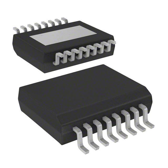
| 供应商器件封装 | PowerSSO-16 |
| 其它名称 | 497-10506-6 |
| 其它有关文件 | http://www.st.com/web/catalog/sense_power/FM1965/CL1969/SC1216/PF248439?referrer=70071840 |
| 包装 | Digi-Reel® |
| 安装类型 | 表面贴装 |
| 导通电阻 | 700 毫欧 |
| 封装/外壳 | 16-PowerFSOP (0.154", 3.90mm 宽) |
| 工作温度 | -40°C ~ 150°C |
| 标准包装 | 1 |
| 电压-电源 | 3 V ~ 5.25 V |
| 电流-峰值输出 | - |
| 电流-输出/通道 | 1.65A |
| 类型 | 高端/低端驱动器 |
| 输入类型 | PWM |
| 输出数 | 6 |


- 商务部:美国ITC正式对集成电路等产品启动337调查
- 曝三星4nm工艺存在良率问题 高通将骁龙8 Gen1或转产台积电
- 太阳诱电将投资9.5亿元在常州建新厂生产MLCC 预计2023年完工
- 英特尔发布欧洲新工厂建设计划 深化IDM 2.0 战略
- 台积电先进制程称霸业界 有大客户加持明年业绩稳了
- 达到5530亿美元!SIA预计今年全球半导体销售额将创下新高
- 英特尔拟将自动驾驶子公司Mobileye上市 估值或超500亿美元
- 三星加码芯片和SET,合并消费电子和移动部门,撤换高东真等 CEO
- 三星电子宣布重大人事变动 还合并消费电子和移动部门
- 海关总署:前11个月进口集成电路产品价值2.52万亿元 增长14.8%


PDF Datasheet 数据手册内容提取
L99MC6 Configurable 6-channel device Features ■ 3 independently self configuring high-/low-side channels ■ 3 low-side channels ■ R =0.7 Ω (typ) at T = 25°C ON j ■ Current limit of each output at min. 0.6 A ■ PWM direct mode PowerSSO-16 ■ Bulb mode with recovery mode ■ LED mode with slew rate control Description ■ Bridge mode with crosscurrent protection ■ SPI interface for data communication The L99MC6 IC is a highly flexible monolithic medium current output driver that incorporates 3 ■ Temperature warning dedicated low-side outputs (channels 4 to 6) and ■ All outputs overtemperature protected 3 independently self configuring outputs ■ All outputs short-circuit protected (channels 1 to 3) that can be used as either low- side or high-side drivers in any combination. The ■ Configurable open-load detection in off mode L99MC6 can control inductive loads, ■ VCC supply voltage 3.0 V to 5.25 V incandescent bulbs or LEDs. ■ Very low current consumption in standby mode The L99MC6 can be used in a half bridge 5µA (typ) configuration with crosscurrent protection. ■ Internal clamp diodes The channel 2 can be controlled directly via the ■ HS switches operate down to 3V crank voltage IN/PWM pin for PWM applications. The IN/PWM signal can be applied to any other output. Applications The integrated 16-bit standard serial peripheral interface (SPI) controls all outputs and provides ■ Relay driver diagnostic information: normal operation, open- ■ LED driver load in off-state, overcurrent, temperature ■ Motor driver warning, overtemperature. ■ Mirror adjustment Table 1. Device summary Order codes Package Part number (tube) Part number (tape & reel) PowerSSO-16 L99MC6-LF L99MC6TR-LF September 2013 Doc ID 16523 Rev 2 1/32 www.st.com 1
Contents L99MC6 Contents 1 Introduction . . . . . . . . . . . . . . . . . . . . . . . . . . . . . . . . . . . . . . . . . . . . . . . . 8 1.1 Application diagram . . . . . . . . . . . . . . . . . . . . . . . . . . . . . . . . . . . . . . . . . . 8 1.2 Block diagram and pin description . . . . . . . . . . . . . . . . . . . . . . . . . . . . . . . 9 2 Description . . . . . . . . . . . . . . . . . . . . . . . . . . . . . . . . . . . . . . . . . . . . . . . . 12 2.1 Dual power supply: V and V . . . . . . . . . . . . . . . . . . . . . . . . . . . . . . . . 12 S CC 2.1.1 Channels . . . . . . . . . . . . . . . . . . . . . . . . . . . . . . . . . . . . . . . . . . . . . . . . 12 2.2 Standby mode . . . . . . . . . . . . . . . . . . . . . . . . . . . . . . . . . . . . . . . . . . . . . 13 2.3 Inductive loads . . . . . . . . . . . . . . . . . . . . . . . . . . . . . . . . . . . . . . . . . . . . . 13 2.4 Diagnostic functions . . . . . . . . . . . . . . . . . . . . . . . . . . . . . . . . . . . . . . . . . 13 2.4.1 Direct input IN/PWM . . . . . . . . . . . . . . . . . . . . . . . . . . . . . . . . . . . . . . . 14 2.4.2 Temperature warning and thermal shutdown . . . . . . . . . . . . . . . . . . . . . 14 2.4.3 Open-load detection in off-state . . . . . . . . . . . . . . . . . . . . . . . . . . . . . . . 14 2.4.4 Overload detection . . . . . . . . . . . . . . . . . . . . . . . . . . . . . . . . . . . . . . . . . 14 2.5 Bridge mode . . . . . . . . . . . . . . . . . . . . . . . . . . . . . . . . . . . . . . . . . . . . . . . 14 2.6 LED mode . . . . . . . . . . . . . . . . . . . . . . . . . . . . . . . . . . . . . . . . . . . . . . . . 15 2.7 Bulb mode (programmable soft start function to drive loads with higher inrush current) . . . . . . . . . . . . . . . . . . . . . . . . . . . . . . . . . . . . . . . . . . . . . 16 3 Absolute maximum ratings . . . . . . . . . . . . . . . . . . . . . . . . . . . . . . . . . . 17 4 ESD protection . . . . . . . . . . . . . . . . . . . . . . . . . . . . . . . . . . . . . . . . . . . . 18 5 Thermal data . . . . . . . . . . . . . . . . . . . . . . . . . . . . . . . . . . . . . . . . . . . . . . 19 5.1 Temperature warning and thermal shutdown . . . . . . . . . . . . . . . . . . . . . . 19 6 Electrical characteristics . . . . . . . . . . . . . . . . . . . . . . . . . . . . . . . . . . . . 20 6.1 Supply . . . . . . . . . . . . . . . . . . . . . . . . . . . . . . . . . . . . . . . . . . . . . . . . . . . 20 6.2 Undervoltage detection . . . . . . . . . . . . . . . . . . . . . . . . . . . . . . . . . . . . . . 20 6.3 Channels . . . . . . . . . . . . . . . . . . . . . . . . . . . . . . . . . . . . . . . . . . . . . . . . . 21 7 SPI electrical characteristics . . . . . . . . . . . . . . . . . . . . . . . . . . . . . . . . . 23 7.1 DC characteristics . . . . . . . . . . . . . . . . . . . . . . . . . . . . . . . . . . . . . . . . . . 23 2/32 Doc ID 16523 Rev 2
L99MC6 Contents 7.2 AC characteristics . . . . . . . . . . . . . . . . . . . . . . . . . . . . . . . . . . . . . . . . . . 23 7.3 Dynamic characteristics . . . . . . . . . . . . . . . . . . . . . . . . . . . . . . . . . . . . . . 24 7.4 SPI timing parameter definition . . . . . . . . . . . . . . . . . . . . . . . . . . . . . . . . 25 8 Functional description of the SPI . . . . . . . . . . . . . . . . . . . . . . . . . . . . . 27 8.1 Signal description . . . . . . . . . . . . . . . . . . . . . . . . . . . . . . . . . . . . . . . . . . . 27 8.1.1 Serial clock (SCK) . . . . . . . . . . . . . . . . . . . . . . . . . . . . . . . . . . . . . . . . . 27 8.1.2 Serial data input (SDI) . . . . . . . . . . . . . . . . . . . . . . . . . . . . . . . . . . . . . . 27 8.1.3 Serial data output (SDO) . . . . . . . . . . . . . . . . . . . . . . . . . . . . . . . . . . . . 27 8.1.4 Chip select not (CSN) . . . . . . . . . . . . . . . . . . . . . . . . . . . . . . . . . . . . . . 27 8.2 SPI communication flow . . . . . . . . . . . . . . . . . . . . . . . . . . . . . . . . . . . . . . 29 8.2.1 General description . . . . . . . . . . . . . . . . . . . . . . . . . . . . . . . . . . . . . . . . 29 8.2.2 Command byte . . . . . . . . . . . . . . . . . . . . . . . . . . . . . . . . . . . . . . . . . . . 29 8.2.3 Global status register . . . . . . . . . . . . . . . . . . . . . . . . . . . . . . . . . . . . . . . 30 8.3 Write operation . . . . . . . . . . . . . . . . . . . . . . . . . . . . . . . . . . . . . . . . . . . . . 32 8.4 Read operation . . . . . . . . . . . . . . . . . . . . . . . . . . . . . . . . . . . . . . . . . . . . . 32 8.5 Read and Clear Status operation . . . . . . . . . . . . . . . . . . . . . . . . . . . . . . . 33 8.6 Read Device Information . . . . . . . . . . . . . . . . . . . . . . . . . . . . . . . . . . . . . 33 9 SPI control and status register . . . . . . . . . . . . . . . . . . . . . . . . . . . . . . . 34 9.1 RAM memory map . . . . . . . . . . . . . . . . . . . . . . . . . . . . . . . . . . . . . . . . . . 34 9.2 ROM memory map (access with OC0 and OC1 set to ‘1’) . . . . . . . . . . . . 34 9.3 Control and status registers . . . . . . . . . . . . . . . . . . . . . . . . . . . . . . . . . . . 34 9.3.1 Channel configuration decoding . . . . . . . . . . . . . . . . . . . . . . . . . . . . . . 36 9.3.2 Register description . . . . . . . . . . . . . . . . . . . . . . . . . . . . . . . . . . . . . . . . 36 9.4 Examples . . . . . . . . . . . . . . . . . . . . . . . . . . . . . . . . . . . . . . . . . . . . . . . . . 37 9.4.1 Example 1:Switch on channel 1 . . . . . . . . . . . . . . . . . . . . . . . . . . . . . . . 37 9.4.2 Example 2: Bridge mode configuration . . . . . . . . . . . . . . . . . . . . . . . . . 38 9.4.3 Example 3: Open-load detection in off-state in bridge configuration . . . 40 10 Maximum demagnetization energy . . . . . . . . . . . . . . . . . . . . . . . . . . . . 42 11 Application examples . . . . . . . . . . . . . . . . . . . . . . . . . . . . . . . . . . . . . . . 45 12 Package and PCB thermal data . . . . . . . . . . . . . . . . . . . . . . . . . . . . . . . 48 12.1 PowerSSO-16 thermal data . . . . . . . . . . . . . . . . . . . . . . . . . . . . . . . . . . . 48 Doc ID 16523 Rev 2 3/32
Contents L99MC6 13 Package and packing information . . . . . . . . . . . . . . . . . . . . . . . . . . . . . 50 13.1 ECOPACK® . . . . . . . . . . . . . . . . . . . . . . . . . . . . . . . . . . . . . . . . . . . . . . . 50 13.2 PowerSSO-16 package information . . . . . . . . . . . . . . . . . . . . . . . . . . . . . 50 13.3 Packing information . . . . . . . . . . . . . . . . . . . . . . . . . . . . . . . . . . . . . . . . . 52 Appendix A Acronyms. . . . . . . . . . . . . . . . . . . . . . . . . . . . . . . . . . . . . . . . . . . . . . 53 Revision history . . . . . . . . . . . . . . . . . . . . . . . . . . . . . . . . . . . . . . . . . . . . . . . . . . . . 54 4/32 Doc ID 16523 Rev 2
L99MC6 List of tables List of tables Table 1. Device summary. . . . . . . . . . . . . . . . . . . . . . . . . . . . . . . . . . . . . . . . . . . . . . . . . . . . . . . . . . 1 Table 2. Pin functions. . . . . . . . . . . . . . . . . . . . . . . . . . . . . . . . . . . . . . . . . . . . . . . . . . . . . . . . . . . . 10 Table 3. Absolute maximum ratings. . . . . . . . . . . . . . . . . . . . . . . . . . . . . . . . . . . . . . . . . . . . . . . . . 17 Table 4. ESD protection . . . . . . . . . . . . . . . . . . . . . . . . . . . . . . . . . . . . . . . . . . . . . . . . . . . . . . . . . . 18 Table 5. Temperature warning and thermal shutdown. . . . . . . . . . . . . . . . . . . . . . . . . . . . . . . . . . . 19 Table 6. Supply. . . . . . . . . . . . . . . . . . . . . . . . . . . . . . . . . . . . . . . . . . . . . . . . . . . . . . . . . . . . . . . . . 20 Table 7. Undervoltage detection. . . . . . . . . . . . . . . . . . . . . . . . . . . . . . . . . . . . . . . . . . . . . . . . . . . . 20 Table 8. Channels. . . . . . . . . . . . . . . . . . . . . . . . . . . . . . . . . . . . . . . . . . . . . . . . . . . . . . . . . . . . . . . 21 Table 9. DC characteristics. . . . . . . . . . . . . . . . . . . . . . . . . . . . . . . . . . . . . . . . . . . . . . . . . . . . . . . . 23 Table 10. AC characteristics. . . . . . . . . . . . . . . . . . . . . . . . . . . . . . . . . . . . . . . . . . . . . . . . . . . . . . . . 23 Table 11. Dynamic characteristic . . . . . . . . . . . . . . . . . . . . . . . . . . . . . . . . . . . . . . . . . . . . . . . . . . . . 24 Table 12. Command byte - general description . . . . . . . . . . . . . . . . . . . . . . . . . . . . . . . . . . . . . . . . . 29 Table 13. Data byte - general description. . . . . . . . . . . . . . . . . . . . . . . . . . . . . . . . . . . . . . . . . . . . . . 29 Table 14. Command byte. . . . . . . . . . . . . . . . . . . . . . . . . . . . . . . . . . . . . . . . . . . . . . . . . . . . . . . . . . 29 Table 15. Operating code definition . . . . . . . . . . . . . . . . . . . . . . . . . . . . . . . . . . . . . . . . . . . . . . . . . . 30 Table 16. Global status register . . . . . . . . . . . . . . . . . . . . . . . . . . . . . . . . . . . . . . . . . . . . . . . . . . . . . 30 Table 17. Global status register description. . . . . . . . . . . . . . . . . . . . . . . . . . . . . . . . . . . . . . . . . . . . 30 Table 18. Command byte for Write mode. . . . . . . . . . . . . . . . . . . . . . . . . . . . . . . . . . . . . . . . . . . . . . 32 Table 19. Command byte for Read mode. . . . . . . . . . . . . . . . . . . . . . . . . . . . . . . . . . . . . . . . . . . . . . 32 Table 20. Command byte for Read and Clear Status operation. . . . . . . . . . . . . . . . . . . . . . . . . . . . . 33 Table 21. Command byte for Read Device Information . . . . . . . . . . . . . . . . . . . . . . . . . . . . . . . . . . . 33 Table 22. RAM memory map . . . . . . . . . . . . . . . . . . . . . . . . . . . . . . . . . . . . . . . . . . . . . . . . . . . . . . . 34 Table 23. ROM memory map. . . . . . . . . . . . . . . . . . . . . . . . . . . . . . . . . . . . . . . . . . . . . . . . . . . . . . . 34 Table 24. Control register 0 . . . . . . . . . . . . . . . . . . . . . . . . . . . . . . . . . . . . . . . . . . . . . . . . . . . . . . . . 34 Table 25. Control register 1 . . . . . . . . . . . . . . . . . . . . . . . . . . . . . . . . . . . . . . . . . . . . . . . . . . . . . . . . 35 Table 26. Control register 2 . . . . . . . . . . . . . . . . . . . . . . . . . . . . . . . . . . . . . . . . . . . . . . . . . . . . . . . . 35 Table 27. Status register 0 . . . . . . . . . . . . . . . . . . . . . . . . . . . . . . . . . . . . . . . . . . . . . . . . . . . . . . . . . 35 Table 28. Status register 1 . . . . . . . . . . . . . . . . . . . . . . . . . . . . . . . . . . . . . . . . . . . . . . . . . . . . . . . . . 35 Table 29. Channel configuration decoding. . . . . . . . . . . . . . . . . . . . . . . . . . . . . . . . . . . . . . . . . . . . . 36 Table 30. Register description . . . . . . . . . . . . . . . . . . . . . . . . . . . . . . . . . . . . . . . . . . . . . . . . . . . . . . 36 Table 31. Command byte - example 1 . . . . . . . . . . . . . . . . . . . . . . . . . . . . . . . . . . . . . . . . . . . . . . . . 37 Table 32. Data byte - example 1. . . . . . . . . . . . . . . . . . . . . . . . . . . . . . . . . . . . . . . . . . . . . . . . . . . . . 37 Table 33. Data byte description - example 1 . . . . . . . . . . . . . . . . . . . . . . . . . . . . . . . . . . . . . . . . . . . 37 Table 34. Command byte 1 - example 2. . . . . . . . . . . . . . . . . . . . . . . . . . . . . . . . . . . . . . . . . . . . . . . 38 Table 35. Data byte 1 - example 2 . . . . . . . . . . . . . . . . . . . . . . . . . . . . . . . . . . . . . . . . . . . . . . . . . . . 38 Table 36. Data byte description 1 - example 2. . . . . . . . . . . . . . . . . . . . . . . . . . . . . . . . . . . . . . . . . . 38 Table 37. Command byte 2 - example 2. . . . . . . . . . . . . . . . . . . . . . . . . . . . . . . . . . . . . . . . . . . . . . . 38 Table 38. Data byte 2 - example 2 . . . . . . . . . . . . . . . . . . . . . . . . . . . . . . . . . . . . . . . . . . . . . . . . . . . 38 Table 39. Data byte description 2 - example 2. . . . . . . . . . . . . . . . . . . . . . . . . . . . . . . . . . . . . . . . . . 39 Table 40. Command byte 1 - example 3. . . . . . . . . . . . . . . . . . . . . . . . . . . . . . . . . . . . . . . . . . . . . . . 40 Table 41. Data byte 1 - example 3 . . . . . . . . . . . . . . . . . . . . . . . . . . . . . . . . . . . . . . . . . . . . . . . . . . . 40 Table 42. Data byte description 1 - example 3. . . . . . . . . . . . . . . . . . . . . . . . . . . . . . . . . . . . . . . . . . 40 Table 43. Command byte 2 - example 3. . . . . . . . . . . . . . . . . . . . . . . . . . . . . . . . . . . . . . . . . . . . . . . 40 Table 44. Data byte 2 - example 3 . . . . . . . . . . . . . . . . . . . . . . . . . . . . . . . . . . . . . . . . . . . . . . . . . . . 40 Table 45. Data byte description 2 - example 3. . . . . . . . . . . . . . . . . . . . . . . . . . . . . . . . . . . . . . . . . . 41 Table 46. Auto and mutual thermal resistance - footprint. . . . . . . . . . . . . . . . . . . . . . . . . . . . . . . . . . 48 Table 47. Auto and mutual thermal resistance - 2 cm2 of Cu heatsink. . . . . . . . . . . . . . . . . . . . . . . . 48 Table 48. Auto and mutual thermal resistance - 8 cm2 of Cu heatsink. . . . . . . . . . . . . . . . . . . . . . . . 49 Doc ID 16523 Rev 2 5/32
List of tables L99MC6 Table 49. PowerSSO-16 mechanical data . . . . . . . . . . . . . . . . . . . . . . . . . . . . . . . . . . . . . . . . . . . . . 51 Table 50. Acronyms . . . . . . . . . . . . . . . . . . . . . . . . . . . . . . . . . . . . . . . . . . . . . . . . . . . . . . . . . . . . . . 53 Table 51. Document revision history . . . . . . . . . . . . . . . . . . . . . . . . . . . . . . . . . . . . . . . . . . . . . . . . . 54 6/32 Doc ID 16523 Rev 2
L99MC6 List of figures List of figures Figure 1. Application diagram . . . . . . . . . . . . . . . . . . . . . . . . . . . . . . . . . . . . . . . . . . . . . . . . . . . . . . . 8 Figure 2. Block diagram. . . . . . . . . . . . . . . . . . . . . . . . . . . . . . . . . . . . . . . . . . . . . . . . . . . . . . . . . . . . 9 Figure 3. Configuration diagram (top view) not in scale. . . . . . . . . . . . . . . . . . . . . . . . . . . . . . . . . . . 11 Figure 4. Power-on reset. . . . . . . . . . . . . . . . . . . . . . . . . . . . . . . . . . . . . . . . . . . . . . . . . . . . . . . . . . 12 Figure 5. Output voltage clamping. . . . . . . . . . . . . . . . . . . . . . . . . . . . . . . . . . . . . . . . . . . . . . . . . . . 13 Figure 6. Example of bridge configuration. . . . . . . . . . . . . . . . . . . . . . . . . . . . . . . . . . . . . . . . . . . . . 15 Figure 7. Example of programmable soft start function for inductive loads and incandescent bulbs. 16 Figure 8. Serial input timing. . . . . . . . . . . . . . . . . . . . . . . . . . . . . . . . . . . . . . . . . . . . . . . . . . . . . . . . 25 Figure 9. Serial input timing. . . . . . . . . . . . . . . . . . . . . . . . . . . . . . . . . . . . . . . . . . . . . . . . . . . . . . . . 25 Figure 10. Output turn on/off delays and slew rates . . . . . . . . . . . . . . . . . . . . . . . . . . . . . . . . . . . . . . 26 Figure 11. Clock polarity and clock phase. . . . . . . . . . . . . . . . . . . . . . . . . . . . . . . . . . . . . . . . . . . . . . 27 Figure 12. SPI frame structure. . . . . . . . . . . . . . . . . . . . . . . . . . . . . . . . . . . . . . . . . . . . . . . . . . . . . . . 28 Figure 13. Indication of the global error flag on DO when CSN is low and SCK is stable. . . . . . . . . . 31 Figure 14. Bridge mode drawing . . . . . . . . . . . . . . . . . . . . . . . . . . . . . . . . . . . . . . . . . . . . . . . . . . . . . 39 Figure 15. Open-load in bridge mode drawing. . . . . . . . . . . . . . . . . . . . . . . . . . . . . . . . . . . . . . . . . . . 41 Figure 16. Configurable switch HSD - maximum turn-off current versus inductance. . . . . . . . . . . . . . 42 Figure 17. Configurable switch LSD - maximum turn-off current versus inductance. . . . . . . . . . . . . . 43 Figure 18. Fixed LSD switch - maximum turn-off current versus inductance. . . . . . . . . . . . . . . . . . . . 44 Figure 19. L99MC6 as driver for incandescent bulb, LEDs and high-side or low-side relays . . . . . . . 45 Figure 20. L99MC6 as motor driver (for example, for mirror adjustment) . . . . . . . . . . . . . . . . . . . . . . 46 Figure 21. L99MC6 as driver for unipolar stepper motor driver, relay and LEDs. . . . . . . . . . . . . . . . . 47 Figure 22. PowerSSO-16 PC board(1). . . . . . . . . . . . . . . . . . . . . . . . . . . . . . . . . . . . . . . . . . . . . . . . . 48 Figure 23. PowerSSO-16 package dimensions. . . . . . . . . . . . . . . . . . . . . . . . . . . . . . . . . . . . . . . . . . 50 Figure 24. PowerSSO-16 tube shipment (no suffix) . . . . . . . . . . . . . . . . . . . . . . . . . . . . . . . . . . . . . . 52 Figure 25. PowerSSO-16 tape and reel shipment (suffix “TR”). . . . . . . . . . . . . . . . . . . . . . . . . . . . . . 52 Doc ID 16523 Rev 2 7/32
Introduction L99MC6 1 Introduction 1.1 Application diagram Figure 1. Application diagram V Bat Active reverse polarity protection VREG Charge Pump PDrroitveecrt iaonnds OL Vcc Config. OUT1 M PWM / IN Driver and OL Protections Config. OUT2 Driver and OL CONTROL Protections Config. OUT3 LOGIC Driver and OL Protections Microcontroller LSD OUT4 Driver and OL Protections LSD OUT5 CSN SCK DI SPI PDrroitveecrt iaonnds OL DO LSD OUT6 GND 8/32 Doc ID 16523 Rev 2
L99MC6 Introduction 1.2 Block diagram and pin description Figure 2. Block diagram Charge VCP VDrive1-3 Open Load Drain [Out1] VOLDVD1rive1-3 OL DRN1 Pump ON/OFF [Out1] Short Circuit [Out1] Open Load Source [Out1] SRC1 VOLS1 VCC Open Load Drain [Out2] VOLD2 DRN2 VDrive1-3 OL ON/OFF [Out2] =1 IN/PWM Short Circuit [Out2] SRC2 Open Load Source [Out2] VOLS2 Open Load Drain [Out3] VOLD3 DRN3 VDrive1-3 OL ON/OFF [Out3] Short Circuit [Out3] Open Load Source [Out3] SRC3 VOLS3 CONTROL LOGIC VCC Open Load Drain [Out4] VOLDV4CC OL DRN4 ON/OFF [Out4] CSN Short Circuit [Out4] SCK SPI Open Load Drain [Out5] VOLDV5CC OL DRN5 ON/OFF [Out5] DI Short Circuit [Out5] 0 DO Open Load Drain [Out6] VOLD6 DRN6 VCC OL ON/OFF [Out6] Short Circuit [Out6] GND Doc ID 16523 Rev 2 9/32
Introduction L99MC6 Table 2. P in functions Pin Symbol Function Ground: 1 / TAB GND Reference potential IN/PWM direct mode: 6 IN/PWM Direct input for channel 2. Other channels can be driven in PWM mode via SPI. Logic voltage supply 3.3V/5V: 8 VCC For this input a ceramic capacitor as close as possible to GND is recommended 3 SRC1 Source of configurable channel 1 4 DRN1 Drain of self configurable channel 1, in HS mode also V supply S 5 DRN2 Drain of self configurable channel 2 15 SRC2 Source of self configurable channel 2 12 DRN3 Drain of self configurable channel 3 13 SRC3 Source of self configurable channel 3 2 DRN4 Drain of channel 4 16 DRN5 Drain of channel 5 14 DRN6 Drain of channel 6 SPI data in: The input requires CMOS logic levels and receives serial data from the 11 DI microcontroller. The data is a 16-bit control word and the most significant bit (MSB, bit7) is transferred first. SPI data out: 9 DO The diagnosis data is available via the SPI and this tristate-output. The output remains in tristate, if the chip is not selected by the input CSN (CSN=high). SPI chip select not (active low): This input is low active and requires CMOS logic levels. The serial data transfer 7 CSN between the L99MC6 and microcontroller is enabled by pulling the input CSN to low-level. SPI serial clock input: 10 SCK This input controls the internal shift register of the SPI and requires CMOS logic levels. 10/32 Doc ID 16523 Rev 2
L99MC6 Introduction Figure 3. Configuration diagram (top view) not in scale 1 16 DRN5 GND 2 15 SRC2 DRN4 3 14 DRN6 SRC1 4 13 SRC3 DRN1 PowerSSO-16 5 12 DRN3 DRN2 6 11 DI PWM/IN 7 8 SCK CSN 8 9 DO VCC The tab must be connected to GND TAB = GND Doc ID 16523 Rev 2 11/32
Description L99MC6 2 Description 2.1 Dual power supply: V and V S CC The supply voltage V (3.3V/5V) supplies the whole device. In case of power-on (V CC CC increases from undervoltage to V =2.7V, typical) the circuit is initialized by an POR OFF internally generated power-on reset (POR). If the voltage V decreases under the CC minimum threshold (V =2.4V, typical), the outputs are switched-off (high- POR ON impedance) and the status registers are cleared (see Figure4). Figure 4. Power-on reset V CC V POROFF V V PORhyst. PORON I is disabled C All Status Registers are cleared 2.1.1 Channels The channels 1 to 3 are self configuring high-side or low-side n-channel mosfets. This flexibility allows the user to connect loads in high-side or low-side configuration in any combination. In order to provide low R values for high-side configured switches (channels 1 to 3), a dson charge pump (CP) to drive the internal gate voltage(s) is implemented. If the charge pump is activated (ENCP1=1, DISCP2=0, see Section9.3: Control and status registers), the internal charge-pump uses V from the drain of channel 1, as its power source. Otherwise S V is used to drive all channels. CC The channels 4 to 6 are n-channel low-side drivers. The source of the respective mosfet are internally connected to the device GND. Caution: For any high-side configuration, channel 1 must be used as a high-side switch. If channel 1 is configured as low-side, the charge pump has to be deactivated to avoid charge pump current from the drain. Caution: The charge pump may not be deactivated (see Section9.3: Control and status registers) if one of the channels is in high-side configuration, while a short-circuit from the source to the battery is present. If these conditions occur, the voltage of the shorted source is applied to the VCC pin. 12/32 Doc ID 16523 Rev 2
L99MC6 Description 2.2 Standby mode The standby mode of the L99MC6 is activated by SPI command (EN bit of CTRL 0 reset to 0, see Section9.3.2: Register description). The inputs and outputs are switched-off. The status registers are cleared and the control registers are reset to their default values. In the standby mode the current consumption is 5µA (typical value). A SPI command is needed to switch the L99MC6 in normal mode. 2.3 Inductive loads Each switch is built by a power DMOS transistor. For low-side configured outputs an internal zener clamp from the drain to gate with a breakdown of 31V minimum provides for fast turn- off of inductive loads. For high-side configured outputs, an internal zener clamp with a breakdown of -15V maximum provides for fast turn-off of inductive loads (Figure5). The maximum clamping energy is specified in Chapter10. Figure 5. Output voltage clamping High Side Configuration Low Side Configuration Output Current DVoraltiang Celamp Drain Voltage VS Output Current (VDRN_CL1-6) = 35V) GND VS Time GND Time Source Clamp Source Voltage Voltage (VSRC_CL1-3) = -19V) 2.4 Diagnostic functions All diagnostic functions (overload, open-load, temperature warning and thermal shutdown) are internally filtered and the condition has to be valid for at least 32µs (open-load: typ. 400µs, respectively) before the corresponding status bit in the status registers are set. The filters are used to improve the noise immunity of the device. Open-load and temperature warning function are intended for information purpose and do not change the state of the output drivers. On contrary, the overload and thermal shutdown condition disable the corresponding driver (overload) or all drivers (thermal shutdown), respectively. Without setting the overcurrent recovery bit in the input data register to logic high, the microcontroller has to clear the overcurrent status bit to reactivate the corresponding driver. (All switches have a corresponding overcurrent recovery bit) If this bit is set, the device automatically switches-on the outputs again after a short recovery time. With this feature the device can drive loads with start-up currents higher than the overcurrent limits (that is inrush current of incandescent lamps, cold resistance of motors and heaters, Figure7). Doc ID 16523 Rev 2 13/32
Description L99MC6 2.4.1 Direct input IN/PWM The IN/PWM input allows channel 2 to be enabled without the use of SPI. The IN/PWM pin is OR-ed with the SPI command bit. This pin can be left open if the channel 2 is controlled only via the SPI. This input has an internal pull-down. The IN/PWM signal can also be applied to any other switches by the activation of the PWM mode. This input is suited for non-inductive loads that are pulse width modulated. This allows PWM control without further use of the SPI. 2.4.2 Temperature warning and thermal shutdown If the junction temperature rises above T a temperature warning flag is set and is j TW detectable via the SPI. If the junction temperature increases above the second threshold T , the thermal shutdown bit is set and power DMOS transistors of all output stages are jSD switched-off to protect the device. Temperature warning flag and thermal shutdown bits are latched. In order to reactivate the output stages, the junction temperature must decrease below T T and the thermal shutdown bit has to be cleared by the jSD- jSDHYS microcontroller. 2.4.3 Open-load detection in off-state The open-load detection monitors the load at each output stage in off mode. A current source of 150µA (I , I ) is connected between drain and source or GND. An OLD1-6 OLS 1-3 open-load failure is detected if the drain or source voltage reaches an internal V OLD/S (2.0V) for at least 3ms (t ). The corresponding open-load bit is set in the status dOL typ. register. In LED mode the open-load detection is disabled and the current source is switched-off, which avoids a turn-on of the LEDs in off-state. 2.4.4 Overload detection In case of an overcurrent condition, a flag is set in the corresponding status register. If the overcurrent signal is valid for at least t =32µs, the overcurrent flag is set and the ISC corresponding driver is switched-off to reduce the power dissipation and to protect the integrated circuit. If the overcurrent recovery bit of the output is zero the microcontroller has to clear the status bit to reactivate the corresponding driver. 2.5 Bridge mode The L99MC6 can be configured as bridge driver. Up to three half bridges can be used. In Bridge mode the device is crosscurrent protected by an internal delay time. If one driver (LS or HS) is turned-off the activation of the other driver of the same half bridge is automatically delayed by the crosscurrent protection time. After the crosscurrent protection time is expired the slew rate limited switch-off phase of the driver is changed to a fast turn-off phase and the opposite driver is turned-on with slew-rate limitation. Due to this behavior it is always guaranteed that the previously activated driver is totally turned-off before the opposite driver starts to conduct. Due to the built-in reverse diodes of the output transistors, inductive loads can be driven at the outputs without external free-wheeling diodes. 14/32 Doc ID 16523 Rev 2
L99MC6 Description The following combination must be used: channel 1 + 4, channel 2 + 5, channel 3 + 6 (Figure6). A V voltage exceeding the low-side clamping voltage (V ) , while the high one of S DRN_CL1-6 the high-side drivers is turned on, may cause a destruction of the device. Caution: In bridge mode using channels 2 and 5, the IN/PWM pin has to be grounded. Therefore PWM mode on other channels is not possible. Figure 6. Example of bridge configuration V 5V DD V 12V S Out1 Out2 IN/PWM =1 M GND Out3 M Control Out4 SCK CSN Out5 SPI DO Out6 DI GND 2.6 LED mode Open-load detection in off-state can be deactivated to avoid the turn on of the LEDs by the current source (150µA typ.) when the channel is switched-off. Moreover, it is possible to select a high slew rate to support PWM operations with small duty cycle (see Section9.3.1: Channel configuration decoding). Doc ID 16523 Rev 2 15/32
Description L99MC6 2.7 Bulb mode (programmable soft start function to drive loads with higher inrush current) Loads with start-up currents higher than the overcurrent limits (for example inrush current of lamps, start current of motors and cold resistance of heaters) can be driven by using the programmable soft start function (that is overcurrent recovery mode). Each driver has a corresponding overcurrent recovery bit. If this bit is set, the device automatically switches- on the outputs again after a fixed recovery time. The PWM modulated current provides sufficient average current to power up the load (for example heat up the bulb) until the load reaches operating condition (Figure6). The device itself cannot distinguish between a real overload and a non linear load like a light bulb. A real overload condition can only be qualified by time. As an example the microcontroller can switch-on light bulbs by setting the overcurrent recovery bit for the first 50ms. After clearing the recovery bit, the output is automatically disabled if the overload condition still exits. Figure 7. Example of programmable soft start function for inductive loads and incandescent bulbs Load Current Load Current Unlimited Inrush Current Unlimited Inrush Current Limited Inrush Current in Limited Inrush Current in overcurrent recovery overcurrent recovery mode mode with inductive load with incandescent bulb t t 16/32 Doc ID 16523 Rev 2
L99MC6 Absolute maximum ratings 3 Absolute maximum ratings Stressing the device above the rating listed in Table3 may cause permanent damage to the device. These are stress ratings only and operation of the device at these or any other conditions above those indicated in the operating sections of this specification is not implied. Exposure to absolute maximum rating conditions for extended periods may affect device reliability. Refer also to the STMicroelectronics™ SURE program and other relevant quality document. T able 3. Absolute maximum ratings Symbol Parameter Value Unit DC supply voltage -0.3 to 28 V V (DRN1 HS Single pulse t < 400ms in HS or LS S max 40 V config) configuration with R = 40 Ω(1) load min Single pulse t < 400ms in bridge mode V V max DRN_CL1-6 V Stabilized supply voltage, logic supply -0.3 to 5.5 V CC DI, DO, SCK, Digital input/output voltage -0.3 to V + 0.3 V CSN, IN CC DRN 1-6 Output current capability ±1,65 A SRC 1-3 Output current capability ±1,65 A GND Current capability 3,30 A T Operating junction temperature -40 to 150 °C j 1. The device requires a minimum load impedance of 40Ω to sustain a load dump pulse of 40V according to the ISO 7637 pulse 5b. All maximum ratings are absolute ratings. Leaving the limitation of any of these values may cause an irreversible damage of the integrated circuit. Doc ID 16523 Rev 2 17/32
ESD protection L99MC6 4 ESD protection T able 4. ESD protection Parameter Value Unit All pins ±2(1) kV Output pins: DRN1 – DRN6; SRC1, SRC3, SRC5 ±4(2) kV Machine model (CDF-AEC-Q100-03 rev. F) ±200 V Charged device model (CDF-AEC-Q100-011 Rev. F) ±1500 V 1. HBM according to MIL883C, Method 3015.7 or EIA/JESD22-A114-A 2. HBM with all unzapped pins grounded 18/32 Doc ID 16523 Rev 2
L99MC6 Thermal data 5 Thermal data 5.1 Temperature warning and thermal shutdown T able 5. Temperature warning and thermal shutdown Item Symbol Parameter Min. Typ. Max. Unit Temperature warning threshold 5.2.1 T T increasing 150 °C jTW ON junction temperature j Temperature warning threshold 5.2.2 T T decreasing 130 °C jTW OFF junction temperature j 5.2.3 T Temperature warning hysteresis - 5 K jTW HYS Thermal shutdown threshold 5.2.4 T T increasing 170 °C jSD ON junction temperature j Thermal shutdown threshold 5.2.5 T T decreasing 150 °C jSD OFF junction temperature j 5.2.6 T Thermal shutdown hysteresis - 5 K jSD HYS For additional information, please refer to Chapter12: Package and PCB thermal data. Doc ID 16523 Rev 2 19/32
Electrical characteristics L99MC6 6 Electrical characteristics V =6V to16V,V =3.0 V to 5.3V,T =-40°C to150°C, unless otherwise specified. S CC j Thevoltages are referred to GND and currents are assumed positive, when the current flows into the pin. 6.1 Supply Table 6. S upply Item Symbol Parameter Test condition Min. Typ. Max. Unit Operating supply voltage 6.1.1 V 6 28 V S range V =13V, V =5.0V S CC active mode 6.1.2 I V DC supply current 1.5 2.0 mA S S DRN1 = V S Outputs floating V =13V, V =5V S CC standby mode DRN1 = V 3 10 μA S 6.1.3 I V quiescent supply current VS S T = -40 °C, 25°C Test Outputs floating T =130°C 6 20 μA Test Operating supply voltage 6.1.4 V 3.0 5.3 V CC range V =13V, V =5.0V 6.1.5 V DC supply current S CC 1.3 2 mA CC active mode V =13V, V =5.0V I S CC CC 6.1.6 VCC quiescent supply CSN=VCC 5 20 µA current standby mode Outputs floating 6.2 Undervoltage detection Table 7. U ndervoltage detection Item Symbol Parameter Test Condition Min. Typ. Max. Unit 6.2.1 V Power-on reset threshold V increasing 3.0 V POR OFF CC 6.2.2 V Power-on reset threshold V decreasing 2.2 V POR ON CC 6.2.3 V Power-on reset hysteresis V - V 0.3 V POR hyst POR OFF POR ON 20/32 Doc ID 16523 Rev 2
L99MC6 Electrical characteristics 6.3 Channels Table 8. C hannels Item Symbol Parameter Test condition Min. Typ. Max. Unit V =13.5V, T =25°C, S j - 700 900 mΩ CP on, I =250mA load V =13.5V, T =125°C, S j - 1100 1500 mΩ CP on, I =250mA load V =6.0V T =25°C, S j - 700 900 mΩ CP on, I =125mA load On resistance drain to V =6.0V, T =125°C, 6.3.1 r S j - 1100 1500 mΩ ON SWI1-3 source in HS configuration CP on, I =125mA load V =4.5V T =25°C, S j - 800 1500 mΩ CP on, I =125mA load V =4.5V, T =125°C, S j - 1300 2000 mΩ CP on, Load=125mA V =3V, T =25°C, S j - 1600 2600 mΩ CP on, I =125mA load V =5.0 V, T =25°C, CC j - 750 1000 mΩ Load=250mA V =5.0V, T =125°C, CC j - 1100 1500 mΩ On resistance drain to I =250mA load 6.3.2 r source or GND, ON SWI1-6 in LS configuration VCC=3.3V, Tj=25°C, - 900 1250 mΩ I =250mA load V =3.3V, T =125°C, CC j - 1400 1800 mΩ I =250mA load Channels 1 to 3 0.7 1.0 1.4 A 6.3.3 I Overcurrent protection SC1-6 Channels 4 to 6 0.6 0.8 1.0 A Output delay time, 6.3.4 t V =13.5V, V =5.0V - 50 100 μs d ON1-6 switch-on S CC Output delay time, 6.3.5 t V =13.5V, V =5.0V - 50 100 μs d OFF1-6 switch-off S CC Output delay time, 6.3.6 t V =13.5V, V =5.0V - 15 40 μs d ONLED1-6 switch-on LED S CC Output delay time, 6.3.7 t V =13.5V, V =5.0V - 15 40 μs dOFFLED1-6 switch-off LED S CC Crosscurrent protection 6.3.8 t Only in Bridge mode - 200 500 μs DHL time V =V , LED mode, Switched-off output current DRN2-6 S 0 - 5 µA 6.3.9 I CP off QLD DRN 1-6 V - 20 µA DRN1 Doc ID 16523 Rev 2 21/32
Electrical characteristics L99MC6 Table 8. Channels (continued) Item Symbol Parameter Test condition Min. Typ. Max. Unit Switched-off output current V =GND, 6.3.10 I SRC1-3 - -15 -25 µA QLS SRC 1-3 LED mode Drain open-load detection 6.3.11 V 1,1 2,0 2,5 V OLD1-6 voltage on drain Open-load detection 6.3.12 I @ V 80 190 280 µA OLD1-6 current on drain OLD Source open-load detection 6.3.13 V 1,1 2,0 2,5 V OLS1-3 voltage on source Open-load detection 6.3.14 I @ V -80 -190 -280 µA OLS1-3 current on source OLS Minimum duration of open- 6.3.15 t load condition to set the Guaranteed by design 2 3 4 ms dOL status bit Minimum duration of 6.3.16 t overcurrent condition to Guaranteed by design 10 - 100 µs ISC switch-off the driver V =13.5V, V =5.0V 6.3.17 dV /dt Slew rate of channel 1 to 6 S CC 0.1 0.25 0.4 V/µs OUT1 I =54Ω load Slew rate of channel 1 to 6 V =13.5V, V =5.0V 6.3.18 dV /dt S CC 0.5 1.25 2.0 V/µs OUT1LED in LED mode I =54 Ω load Drain clamp voltage Source = GND 6.3.19 V 31 35 39 V DRN_CL1-6 (low-side) I =0.25A load Source clamp voltage Drain = VS, Iload=0.25A -22 -19 -15 V 6.3.20 V SRC_CL1-3 (high-side) Standby -22 10 -1,5 V 22/32 Doc ID 16523 Rev 2
L99MC6 SPI electrical characteristics 7 SPI electrical characteristics V =6V to16V,V =3.0V to 5.3V,T =-40°C to150°C,unless otherwise specified. S CC j Thevoltages are referred to GND and currents are assumed positive, when the current flows into the pin 7.1 DC characteristics Table 9. D C characteristics Symbol Parameter Test condition Min Typ Max Unit DI, SCK, CSN, PWM V Low-level input voltage - 0.3V V IL DD V High-level input voltage - 0.7V V IH DD R Pull-up resistor at input CSN - 20 50 80 kΩ CSN in R Pull-down resistor at input CLK - 20 50 80 kΩ CLK in R Pull-down resistor at input DI - 20 50 80 kΩ DI in DO V Low-level output voltage I = 5mA 0.3V V OL OUT DD V High-level output voltage I = 5mA 0.7V V OH OUT DD 7.2 AC characteristics Table 10. A C characteristics Symbol Parameter Test condition Min Typ Max Unit DI, DO, SCK, CSN C Output capacitance (DO) V = 0 to 5V - - 10 pF OUT OUT Input capacitance (DI) V = 0 to 5V - - 10 pF IN C IN Input capacitance (other pins) V = 0 to 5V - - 10 pF IN Doc ID 16523 Rev 2 23/32
SPI electrical characteristics L99MC6 7.3 Dynamic characteristics Table 11. D ynamic characteristic Symbol Parameter Test condition Min Typ Max Unit f Clock frequency - - - 1 MHz C t CSN low setup time see Figure8 120 - - ns SCSN t CSN high setup time see Figure8 1 - - μs HCSN t CSN falling until DO valid - 5 130 250 ns CSNQV t CSN rising until DO tristate - 150 650 1000 ns CSNQT SCK setup time before CSN t - 200 - - ns SSCK rising t Data in setup time see Figure8 20 - - ns SSDI t Data hold setup time see Figure8 30 - - ns CHDX t SCK high time see Figure8 115 - - ns HSCK t SCK low time see Figure8 115 - - ns LSCK t Clock high to output valid C = 100pF - 150 - ns SCKQV OUT t Output rise time C = 100pF - 110 - ns QLQH OUT t Output fall time C = 100pF - 110 - ns QHQL OUT DO enable time from tristate to C = 100pF, I = -1mA, t OUT OUT - 100 250 ns enDOtriH high-level pull-down load to GND DO enable time from tristate to C = 100pF, I =1mA, t OUT OUT - 100 250 ns enDOtriL low-level pull-up load to V CC DO disable time from high-level C = 100pF, I = -4mA, t OUT OUT - 625 720 ns disDOHtri to tristate pull-down load to GND DO disable time from low-level C = 100pF, I =4mA, t OUT OUT - 540 620 ns disDOLtri to tristate pull-up load to V CC 24/32 Doc ID 16523 Rev 2
L99MC6 SPI electrical characteristics 7.4 SPI timing parameter definition Figure 8. Serial input timing t HCSN CSN t CSNQV t CSNQT Data out Data out SDO t t t SCKQV SSCK SCSN SCK t t t SSDI HSCK LSCK SDI Data in Data in Figure 9. Serial input timing CSN SDO pull-up load to VCC C =100pF L t t enDO tri L disDO L tri SDO pull-down load to GND C =100pF L t t enDO tri H disDO H tri Doc ID 16523 Rev 2 25/32
SPI electrical characteristics L99MC6 Figure 10. Output turn on/off delays and slew rates V V V IN/PWM INIPWM DD V DD 50% 50% GND GND Vsource X Vsource X Lowside 90% 80% Lowside 90% 20% 10% 20% GND GND V V drain X drain X 90% High Side 80% High Side 80% 20% 20% 10% GND Tdon1-6 Tdoff1-6 dVout1x/dt dVout1x/dt 26/32 Doc ID 16523 Rev 2
L99MC6 Functional description of the SPI 8 Functional description of the SPI 8.1 Signal description 8.1.1 Serial clock (SCK) This input signal provides the timing of the serial interface. Data present at serial data input (SDI) is latched on the rising edge of serial clock (SCK). Data on serial data output (SDO) is shifted out at the falling edge of serial clock (see Figure11). The SPI can be driven by a microcontroller with its SPI peripherals running in following mode: CPOL=0 and CPHA=0 (see Figure11). 8.1.2 Serial data input (SDI) This input is used to transfer data serially into the device. It receives the data to be written. Values are latched on the rising edge of serial clock (SCK). 8.1.3 Serial data output (SDO) This output signal is used to transfer data serially out of the device. Data is shifted out on the falling edge of serial clock (SCK). DO also reflects the status of the <Global Error Flag> (<Global Status Register>, bit 7) while CSN is low and no clock signal is present 8.1.4 Chip select not (CSN) When this input signal is high, the device is deselected and serial data output (SDO) is high- impedance. Driving this input low enables the communication. The communication must start and stop on a low-level of serial clock (SCK). Figure 11. Clock polarity and clock phase Doc ID 16523 Rev 2 27/32
Functional description of the SPI L99MC6 Figure 12. SPI frame structure SPI-Frame Structure Write Operation CSN Command Byte Data SDI (8 bit) (8, 16 or 24 bit) MSB LSB MSB LSB Global Status Byte Data SDO (previous content of register) (8 bit) MSB LSB Read Operation CSN Command Byte Don’t care SDI (8 bit) (8, 16 or 24 bit) MSB LSB MSB LSB Data Global Status Byte SDO (8, 16 or 24 bit) (8 bit) MSB LSB 28/32 Doc ID 16523 Rev 2
L99MC6 Functional description of the SPI 8.2 SPI communication flow 8.2.1 General description The proposed SPI communication is based on a standard SPI interface structure using CSN (chip select not), SDI (serial data in), SDO (serial data out/error) and SCK (serial clock) signal lines. At the beginning of each communication the master reads the <SPI-frame-ID> register (ROM address 3EH) of the slave device. This 8-bit register indicates the SPI frame length (16 bit for the L99MC6) and the availability of additional features. Each communication frame consists of an instruction byte which is followed by 1 data byte (see Figure12). The data returned on SDO within the same frame always starts with the <Global Status> register. It provides general status information about the device. It is followed by 1 byte (that is ‘In-frame-response’, see Figure12). For Write cycles the <Global Status> register is followed by the previous content of the addressed register. For Read cycles the <Global Status> register is followed by the content of the addressed register. T able 12. Command byte - general description MSB LSB Operating code Address OC1 OC0 A5 A4 A3 A2 A1 A0 T able 13. Data byte - general description MSB LSB Bit7 Bit6 Bit5 Bi4 Bit3 Bit2 Bit1 Bit0 8.2.2 Command byte Each communication frame starts with a command byte. It consists of an operating code which specifies the type of operation (<Read>, <Write>, <Read and Clear Status>, <Read Device Information>) and a 6-bit address. T able 14. Command byte MSB LSB Operating code Address OC1 OC0 A5 A4 A3 A2 A1 A0 Doc ID 16523 Rev 2 29/32
Functional description of the SPI L99MC6 Operating code definition T able 15. Operating code definition OC1 OC0 Meaning 0 0 <Write mode> 0 1 <Read mode> 1 0 <Read and Clear Status> 1 1 <Read Device Information> The <Write mode> and <Read mode> operations allow access to the RAM of the device, that is write to control registers or read status information. A <Read and Clear Status> operation addressed to a device specific status register reads back and subsequently clear this status register. A <Read and Clear Status> operation with address 3FH clears all status registers at a time. A <Read and Clear Status> operation addressed to an unused RAM address or configuration register address is identical to a <Read mode> operation (in case of unused RAM address, the second byte is equal to 00H). <Read Device Information> allows access to the ROM area which contains device related information such as the product family, product name, silicon version and register width. 8.2.3 Global status register Table 16. G lobal status register Bit 7 Bit 6 Bit 5 Bit 4 Bit 3 Bit 2 Bit 1 Bit 0 Global error flag Communication TSD Temperature Open-load Overcurrent Chip reset Unused (GEF) error Chip overload warning detected detected T able 17. Global status register description Bit Description Polarity Comment 0 Unused Active high Always returns ‘0’ 1 Overcurrent detected Active high Set by any overcurrent event 2 Open-load detected Active high Set by any open-load event 3 Temperature warning Active high - Thermal shutdown / chip 4 Active high - overload Activated by all internal reset events that change device state or configuration registers (for example software reset, V undervoltage, etc.). 5 Chip reset Active low CC The bit is cleared after a valid communication with any register. This bit is initially ‘0’ and is set to ‘1’ by a valid SPI communication 30/32 Doc ID 16523 Rev 2
L99MC6 Functional description of the SPI Table 17. Global status register description (continued) Bit Description Polarity Comment Bit is set if the number of clock cycles during CSN=low does not match with the specified frame width or if an invalid bus condition is 6 Communication error Active high detected (DI always 1). DI always 0 automatically leads to clearing the enable bit in CTRL0 and is not signaled as communication error. Logic OR combination of all failures in the 7 Global Error flag Active high <Global Status Byte>. The <Global Error Flag> is generated by an OR-combination of all failure events of the device (that is <Global Status Register>, [0:6]). Figure 13. Indication of the global error flag on DO when CSN is low and SCK is stable 1. The last transferred SPI command is still valid in the input shift register. If SCK is stable (high or low) during a CSN low pulse, at the rising edge of CSN the last transferred SPI command is still valid in the input shift register and is repeated. Therefore, it is recommended to send a complete SPI frame to monitor the status of the L99MC6. Writing to the selecteddatainputregister is only enabled if exactlyone frame lengthis transmitted within one communication frame (that is CSN low). If more or less clock pulses are counted within one frame, the complete frame is ignored and a SPI frame error is signaled in the Global Status register. This safety function is implemented to avoid anunwanted activation of output stages by a wrong communication frame. Doc ID 16523 Rev 2 31/32
Functional description of the SPI L99MC6 For Read operations, the <communication error> bit in the <Global Status Register> is set, but the register to be read is still transferred to the DO pin. If the number of clock cycles is smaller than the frame width, the data at DO is truncated. If the number of clock cycles is larger than the frame width, the data at DO is filled with ‘0’ bits. Due to this safety functionality a daisy chaining of SPI is not possible. Instead, a parallel operation of the SPI bus by controlling the CSN signal of the connected ICs is recommended. Note: If the frame width is greater than 16 bits, initial Read of <SPI-frame-ID> using a 16-bit communication sets the <communication Error bit> of the <Global Status> register. A subsequent correct length transaction is necessary to correct this bit. 8.3 Write operation OC0, OC1: operating code (00 for ‘Write’ mode) T able 18. Command byte for Write mode MSB LSB Operating code Address 0 0 A5 A4 A3 A2 A1 A0 The Write operation starts with a command byte followed by 1 data byte. For Write cycles the <Global Status> register is followed by the previous content of the addressed register. The RAM memory area consists of 8-bit registers. All unused RAM addresses are read as ‘0’. Failures are indicated by activating the corresponding bit of the <Global Status> register. Note: The register definition for RAM address 00H is device specific. A register value of all 0 causes a device reset (interpreted as ‘Data-in short to GND’). 8.4 Read operation OC0, OC1: operating code (01 for ‘Read’ mode) T able 19. Command byte for Read mode MSB LSB Operating code Address 0 1 A5 A4 A3 A2 A1 A0 The Read operation starts with a command byte followed by 1 data byte. The content of the data byte is ‘do not care’. The content of the addressed register is shifted out at SDO within the same frame (‘in-frame response’). The returned data byte represents the content of the register to be read. Failures are indicated by activating the corresponding bit of the <Global Status> register. 32/32 Doc ID 16523 Rev 2
L99MC6 Functional description of the SPI 8.5 Read and Clear Status operation OC0, OC1: operating code (10 for ‘Read and Clear Status’ mode) T able 20. Command byte for Read and Clear Status operation MSB LSB Operating code Address 1 0 A5 A4 A3 A2 A1 A0 The ‘Read and Clear Status’ operation starts with a command byte followed by 1 data byte. The content of the data byte is ‘do not care’. The content of the addressed status register is transferred to SDO within the same frame (‘in-frame response’) and is subsequently cleared. A <Read and Clear Status> operation with address 3FH clears all status registers simultaneously. A <Read and Clear Status> operation addressed to an unused RAM address or to the configuration register (3FH) is identical to a <Read mode> operation (in case of unused RAM address, the second byte is equal to 00H). The returned data byte represents the content of the register to be read. Failures are indicated by activating the corresponding bit of the <Global Status> register. 8.6 Read Device Information OC0, OC1: operating code (11 for ‘Read Device Information’ mode) T able 21. Command byte for Read Device Information MSB LSB Operating code Address 1 1 A5 A4 A3 A2 A1 A0 The device information is stored at the ROM. In the ROM memory area, the first 8 bits are used. All unused ROM addresses is read as ‘0’. Note: ROM address 3FH is unused. An attempt to access this address is recognized as a communication line error (‘Data-in stuck to V ’) and the standby mode is automatically CC entered (all internal registers are cleared). Doc ID 16523 Rev 2 33/32
SPI control and status register L99MC6 9 SPI control and status register 9.1 RAM memory map T able 22. RAM memory map Address Name Access Content 00h CTRL 0 Read/Write Global enable, channels 3 and 6 control register 01h CTRL 1 Read/Write CP, channels 2 and 5 control register 02h CTRL 2 Read/Write CP, channels 1 and 4 control register 03h Unused - - 04h STAT 0 Read only Open-load / thermal status register 05h STAT 1 Read only Overcurrent / thermal status register 9.2 ROM memory map (access with OC0 and OC1 set to ‘1’) T able 23. ROM memory map Address Name Access Content 00h ID Header Read only 42h (device class ASSP, 2 additional information bytes) 01h Product ID Read only 06H Category / 18h (multi channel driver, 02h Read only Version last 3 LSB = 0: engineering samples) 3Eh SPI-Frame ID Read only 01h (no burst mode, no watchdog, 16 bit frame SPI) 9.3 Control and status registers Table 24. C ontrol register 0 Data Byte Adress Access Bit 7 Bit 6 Bit 5 Bit 4 Bit 3 Bit 2 Bit 1 Bit 0 Global enable, Channel 3&6 control CH6 CH6 CH6 Bridge CH3 CH3 CH3 00h R/W EN [2] [1] [0] 3&6 [2] [1] [0] Default 0 0 0 0 0 0 0 0 34/32 Doc ID 16523 Rev 2
L99MC6 SPI control and status register Table 25. C ontrol register 1 Data Byte Adress Access Bit 7 Bit 6 Bit 5 Bit 4 Bit 3 Bit 2 Bit 1 Bit 0 Channel 2&5 control CH5 CH5 CH5 Bridge CH2 CH2 CH2 01h R/W ENCP [2] [1] [0] 2&5 [2] [1] [0] Default 1 0 0 0 0 0 0 0 Table 26. C ontrol register 2 Data Byte Adress Access Bit 7 Bit 6 Bit 5 Bit 4 Bit 3 Bit 2 Bit 1 Bit 0 Channel 1&4 control CH4 CH4 CH4 Bridge CH1 CH1 CH1 02h R/W DISCP [2] [1] [0] 1&4 [2] [1] [0] Default 0 0 0 0 0 0 0 0 Table 27. S tatus register 0 Data Byte Adress Access Bit 7 Bit 6 Bit 5 Bit 4 Bit 3 Bit 2 Bit 1 Bit 0 Open-load, thermal status OL OL OL OL OL OL 04h R TSD TWARN CH6 CH5 CH4 CH3 CH2 CH1 Table 28. S tatus register 1 Data Byte Adress Access Bit 7 Bit 6 Bit 5 Bit 4 Bit 3 Bit 2 Bit 1 Bit 0 Overcurrent, thermal status OC OC OC OC OC OC 05h R TSD TWARN CH6 CH5 CH4 CH3 CH2 CH1 Doc ID 16523 Rev 2 35/32
SPI control and status register L99MC6 9.3.1 Channel configuration decoding Table 29. C hannel configuration decoding CHx CHx CHx PWM Overcurrent Open-load CHx Slew Rate [2] [1] [0] mode recovery detection 0 0 0 Off(1) No - High Off 1 1 1 Off(1) No - Low On 0 0 1 On No No High - 0 1 0 On No No Low - 0 1 1 On No Yes Low - 1 0 1 IN/PWM(2) Yes No High Off 1 1 0 IN/PWM(2) Yes No Low On 1. The state of the channel 2 is according to the IN/PWM signal 2. The output state is according to the IN/PWM signal, note that bridge mode and PWM mode may not be activated at the same time for channels 2 and 5. 9.3.2 Register description Table 30. R egister description(1) Name Comment EN Global device enable bit. If this bit is reset, the device goes in standby mode. Channel output configuration (see Figure29). CHx Note that channel 2 is directly driven by the external IN/PWM pin and thus can not be configured [2:0] independently from the PWM configuration of other channels. Activate Bridge mode between channels 3 and 6, channels 2 and 5, channels 1 and 4. Any polarity change is delayed by masking time of cross conduction protection Bridge If wrong SPI commands try to turn on the channels 3 and 6, channels 2 and 5, channels 1 and 4 simultaneously, the high-side (channels 3, 2, 1) has the priority whereas channels 6, 5, 4 is (or stay) deactivated. This bit is preset to ‘1’ at startup. To deactivate the internal charge pump ENCP has to be reset together with setting DISCP (CTRL 2). This mechanism avoids unwanted charge pump ENCP deactivation after an undetected communication error. It is recommended to check the state of the charge pump deactivation bits at every access of CTRL 1 and CTRL 2. This bit is reset to ‘0’ at startup. To deactivate the internal charge pump DISCP has to be set DISCP together with resetting ENCP (CTRL 1) TSD Overtemperature detected: all the drivers are shutdown TWARN Overtemperature warning level detected, information only OL [6:1] Open-load error detected, information only Overcurrent error detected, drivers are deactivated and re-enabled cyclically when bulb mode is OC [6:1] configured. Note: in order to detect a real overload condition, the application software must make sure, that the corresponding OC bit remains cleared after a maximum heat up time of the load. 1. Every output stage is protected against overtemperature and overcurrent. While still configured as ON, the output stage can be deactivated by the corresponding error bits in the status registers. In order to reactivate the drivers, the status registers have to be cleared by a specific SPI command. 36/32 Doc ID 16523 Rev 2
L99MC6 SPI control and status register 9.4 Examples 9.4.1 Example 1:Switch on channel 1 It is assumed that the charge pump is already activated (ENCP1=1 and DISCP2=0, POR default) T able 31. Command byte - example 1 MSB LSB Operating code Address 0 0 0 0 0 0 1 0 T able 32. Data byte - example 1 MSB LSB 0 0 0 0 0 0 0 1 From Table31 and Table32 follow that the value 01h is written at RAM address 02h (control register 2). Table33 describe more in detail the data byte structure. T able 33. Data byte description - example 1 CH4 CH4 CH4 Bridge CH1 CH1 CH1 DISCP [2] [1] [0] 1&4 [2] [1] [0] 0 0 0 0 0 0 0 1 Hereafter the actions linked to each value of bit or group of bits: ● DISCP = 0: Charge pump stays activated ● CH4[2:0] = 000b: Channel 4 is off, open-load detection in off-state disabled ● BRIDGE_1&4 = 0: Bridge mode disabled ● CH4[2:0] = 001b: Channel 1 is on, high slew rate, PWM not activated, overcurrent recovery deactivated. Doc ID 16523 Rev 2 37/32
SPI control and status register L99MC6 9.4.2 Example 2: Bridge mode configuration T able 34. Command byte 1 - example 2 MSB LSB Operating code Address 0 0 0 0 0 0 0 1 T able 35. Data byte 1 - example 2 MSB LSB 1 0 1 0 1 0 0 0 From Table34 and Table35 follow that the value A8h is written at RAM address 01h (control register 1). Table36 describe more in detail the data byte structure. T able 36. Data byte description 1 - example 2 CH5 CH5 CH5 Bridge CH2 CH2 CH2 ENCP [2] [1] [0] 2&5 [2] [1] [0] 1 0 1 0 1 0 0 0 Hereafter the actions linked to each value of bit or group of bits: ● ENCP = 1: Charge pump stays activated ● CH5[2:0] = 010b: Channel 5 is on, PWM disabled, overcurrent recovery mode disabled, low slew rate ● BRIDGE_2&5 = 1: Bridge mode for channel 2 and channel 5 activated ● CH2[2:0] = 000b: Channel 2 is off, open-load detection in off-state disabled T able 37. Command byte 2 - example 2 MSB LSB Operating code Address 0 0 0 0 0 0 1 0 T able 38. Data byte 2 - example 2 MSB LSB 0 0 0 0 1 0 1 0 From Table37 and Table38 follow that the value 0Ah is written at RAM address 02h (control register 2). Table39 describe more in detail the data byte structure. 38/32 Doc ID 16523 Rev 2
L99MC6 SPI control and status register T able 39. Data byte description 2 - example 2 CH4 CH4 CH4 Bridge CH1 CH1 CH1 DISCP [2] [1] [0] 1&4 [2] [1] [0] 0 0 0 0 1 0 1 0 Hereafter the actions linked to each value of bit or group of bits: ● DISCP = 0: Charge pump stays activated ● CH4[2:0] = 000b: Channel 4 is off, open-load detection in off-state disabled ● BRIDGE_1&4 = 1: Bridge mode for channel 1 and channel 4 activated ● CH4[2:0] = 010b: Channel 1 is on, PWM disabled, overcurrent recovery mode disabled, low slew rate Figure 14. Bridge mode drawing Vs CH1 ON CH 2 OFF M CH4 OFF CH 5 ON Doc ID 16523 Rev 2 39/32
SPI control and status register L99MC6 9.4.3 Example 3: Open-load detection in off-state in bridge configuration T able 40. Command byte 1 - example 3 MSB LSB Operating code Address 0 0 0 0 0 0 0 1 T able 41. Data byte 1 - example 3 MSB LSB 1 1 1 1 1 0 0 0 From Table40 and Table41 follow that the value F8h is written at RAM address 01h (control register 1). Table42 describe more in detail the data byte structure. T able 42. Data byte description 1 - example 3 CH5 CH5 CH5 Bridge CH2 CH2 CH2 ENCP [2] [1] [0] 2&5 [2] [1] [0] 1 1 1 1 1 0 0 0 Hereafter the actions linked to each value of bit or group of bits: ● ENCP = 1: Charge pump stays activated ● CH5[2:0] = 111b: Channel 5 is off, open-load detection in off-state enabled ● BRIDGE_2&5 = 1: Bridge mode for channel 2 and channel 5 activated ● CH2[2:0] = 000b: Channel 2 is off, open-load detection in off-state disabled T able 43. Command byte 2 - example 3 MSB LSB Operating code Address 0 0 0 0 0 0 1 0 T able 44. Data byte 2 - example 3 MSB LSB 0 0 0 0 1 0 1 0 From Table43 and Table44 follow that the value 0Ah is written at RAM address 02h (control register 2). Table45 describe more in detail the data byte structure. 40/32 Doc ID 16523 Rev 2
L99MC6 SPI control and status register T able 45. Data byte description 2 - example 3 CH4 CH4 CH4 Bridge CH1 CH1 CH1 DISCP [2] [1] [0] 1&4 [2] [1] [0] 0 0 0 0 1 0 1 0 Hereafter the actions linked to each value of bit or group of bits: ● DISCP = 0: Charge pump stays activated ● CH4[2:0] = 000b: Channel 4 is off, open-load detection in off-state disabled ● BRIDGE_1&4 = 1: Bridge mode for channel 1 and channel 4 activated ● CH1[2:0] = 010b: Channel 1 is on, PWM disabled, overcurrent recovery mode disabled, low slew rate Figure 15. Open-load in bridge mode drawing Vs CH1 ON CH2 OFF OL detection OFF OL detection OFF M CH4 OFF CH5 OFF OL detection OFF OL detection ON There are two operating conditions: ● Case 1: The motor is connected, drain of channel 5 is pulled up by channel 1 (on) through the motor, then no open-load detected on channel 5 ● Case 2: The motor is not connected and the drain voltage of channel 5 is below the open-load threshold, then open-load detected on channel 5 Doc ID 16523 Rev 2 41/32
Maximum demagnetization energy L99MC6 10 Maximum demagnetization energy Figure 16. Configurable switch HSD - maximum turn-off current versus inductance 1 A B C A) ( I 0.1 100 L (mH) 1000 A: Single pulse, T = 150 °C j B: Repetitive pulse, T = 100 °C j C: Repetitive pulse, T = 125 °C j 42/32 Doc ID 16523 Rev 2
L99MC6 Maximum demagnetization energy Figure 17. Configurable switch LSD - maximum turn-off current versus inductance 1 A B C A) ( I 0.1 100 L (mH) 1000 A: Single pulse, T = 150 °C j B: Repetitive pulse, T = 100 °C j C: Repetitive pulse, T = 125 °C j Doc ID 16523 Rev 2 43/32
Maximum demagnetization energy L99MC6 Figure 18. Fixed LSD switch - maximum turn-off current versus inductance 1 A B C A) ( I 0.1 100 L (mH) 1000 A: Single pulse, T = 150 °C j B: Repetitive pulse, T = 100 °C j C: Repetitive pulse, T = 125 °C j 44/32 Doc ID 16523 Rev 2
L99MC6 Application examples 11 Application examples Figure 19. L99MC6 as driver for incandescent bulb, LEDs and high-side or low-side relays V 5V DD V 12V S Out1 Out2 IN/PWM =1 Out3 Control Out4 SCK CSN Out5 SPI DO DI Out6 GND Doc ID 16523 Rev 2 45/32
Application examples L99MC6 Figure 20. L99MC6 as motor driver (for example, for mirror adjustment) V 5V DD V 12V S Out1 Out2 IN/PWM =1 M GND Out3 M Control Out4 SCK CSN Out5 SPI DO Out6 DI GND 46/32 Doc ID 16523 Rev 2
L99MC6 Application examples Figure 21. L99MC6 as driver for unipolar stepper motor driver, relay and LEDs VDD 5V VS12V Out1 Out2 IN/PWM =1 Out3 Control Out4 SCK SM CSN Out5 SPI DO Out6 DI GND Doc ID 16523 Rev 2 47/32
Package and PCB thermal data L99MC6 12 Package and PCB thermal data 12.1 PowerSSO-16 thermal data Figure 22. PowerSSO-16 PC board(1) . 1. Layout condition of thermal resistance measurements (PCB: double layer, thermal vias, FR4 area = 77 mm x 86 mm, PCB thickness =1.6 mm, Cu thickness = 70 µm (front and back side) thermal vias separation 1.2 mm, thermal via diameter 0.3 mm +/- 0.08 mm, Cu thickness on vias 25 µm, footprint dimension 2.5 mm x 4.2 mm ). T able 46. Auto and mutual thermal resistance - footprint HSD 1 HSD 2 HSD 3 LSD 4 LSD 5 LSD 6 HSD 1 89.57 85.83 84.41 88.89 87.06 85.84 HSD 2 85.83 89.57 84.41 87.06 88.89 87.06 HSD 3 84.41 84.41 89.57 85.84 87.06 88.89 LSD 4 88.89 87.06 85.84 93.58 90.54 89.08 LSD 5 87.06 88.89 87.06 90.54 93.58 90.54 LSD 5 85.84 87.06 88.89 89.08 90.54 93.58 T able 47. Auto and mutual thermal resistance - 2 cm2 of Cu heatsink HSD 1 HSD 2 HSD 3 LSD 4 LSD 5 LSD 6 HSD 1 59.96 55.06 54.23 58.25 56.08 54.71 HSD 2 55.06 59.96 54.23 56.08 58.25 56.08 HSD 3 54.23 54.23 59.96 54.71 56.08 58.25 LSD 4 58.25 56.08 54.71 61.80 60.37 59.45 LSD 5 56.08 58.25 56.08 60.37 61.80 60.37 LSD 5 54.71 56.08 58.25 59.45 60.37 61.80 48/32 Doc ID 16523 Rev 2
L99MC6 Package and PCB thermal data T able 48. Auto and mutual thermal resistance - 8 cm2 of Cu heatsink HSD 1 HSD 2 HSD 3 LSD 4 LSD 5 LSD 6 HSD 1 46.51 43.16 41.49 45.19 43.06 42.08 HSD 2 43.16 46.51 41.49 43.06 45.19 43.06 HSD 3 41.49 41.49 46.51 42.08 43.06 45.19 LSD 4 45.19 43.06 42.08 47.19 46.31 45.19 LSD 5 43.06 45.19 43.06 46.31 47.19 46.31 LSD 5 42.08 43.06 45.19 45.19 46.31 47.19 Δ Equation 1 represents T calculation of a full loaded device for the HSD1 junction. j-amb Equation 1 ΔT =Rth ∗Pd +Rth ∗Pd +Rth ∗Pd + HSD1 HSD1 HSD1 HSD1,HSD2 HSD2 HSD1,HSD3 HSD3 +Rth ∗Pd +Rth ∗Pd +Rth ∗Pd HSD1,LSD4 LSD4 HSD1,LSD5 LSD5 HSD1,LSD6 LSD6 Doc ID 16523 Rev 2 49/32
Package and packing information L99MC6 13 Package and packing information ® 13.1 ECOPACK In order to meet environmental requirements, ST offers these devices in different grades of ECOPACK® packages, depending on their level of environmental compliance. ECOPACK® specifications, grade definitions and product status are available at: www.st.com. ECOPACK® is an ST trademark. 13.2 PowerSSO-16 package information Figure 23. PowerSSO-16 package dimensions 50/32 Doc ID 16523 Rev 2
L99MC6 Package and packing information T able 49. PowerSSO-16 mechanical data(1) Millimeters Symbol Min. Typ. Max. A 1.25 - 1.72 A1 0.00 - 0.10 A2 1.10 - 1.62 B 0.18 - 0.36 C 0.19 - 0.25 D(2) 4.80 - 5.00 E 3.80 - 4.00 e - 0.50 - H 5.80 - 6.20 h 0.25 - 0.50 L 0.40 - 1.27 k 0d - 8d X 1.90 - 2.50 Y 3.60 - 4.20 ddd - 0.10 1. Drawings dimensions include single and matrix versions. 2. Dimensions D does not include mold flash protrusions or gate burrs. Mold flash protrusions or gate burrs shall not exceed 0.15mm in total (both side). Doc ID 16523 Rev 2 51/32
Package and packing information L99MC6 13.3 Packing information Figure 24. PowerSSO-16 tube shipment (no suffix) B C Base Q.ty 100 Bulk Q.ty 2000 Tube length (± 0.5) 532 A 1.85 A B 6.75 C (± 0.1) 0.6 All dimensions are in mm. Figure 25. PowerSSO-16 tape and reel shipment (suffix “TR”) REEL DIMENSIONS Base q.ty 2500 Bulk q.ty 2500 A (max) 330 B (min) 1.5 C (± 0.2) 13 F 20.2 G (+ 2 / -0) 12.4 N (min) 60 T (max) 18.4 TAPE DIMENSIONS According to Electronic Industries Association (EIA) Standard 481 rev. A, Feb. 1986 Tape width W 12 Tape hole spacing P0 (± 0.1) 4 Component spacing P 8 Hole diameter D (± 0.05) 1.5 Hole diameter D1 (min) 1.5 Hole position F (± 0.1) 5.5 Compartment depth K (max) 4.5 Hole spacing P1 (± 0.1) 2 End All dimensions are in mm. Start Top No components Components No components cover tape 500mm min 500mm min Empty components pockets saled with cover tape. User direction of feed 52/32 Doc ID 16523 Rev 2
L99MC6 Acronyms Appendix A Acronyms T able 50. Acronyms Acronym Name CSN Chip select not CTRL Control register POR Power-on reset SCK Serial clock SDI Serial data input SDO Serial data output SPI Serial peripheral interface SR Slew rate STAT Status register Doc ID 16523 Rev 2 53/32
Revision history L99MC6 Revision history T able 51. Document revision history Date Revision Changes 18-Nov-2009 1 Initial release. 20-Sep-2013 2 Updated disclaimer. 54/32 Doc ID 16523 Rev 2
L99MC6 Please Read Carefully: Information in this document is provided solely in connection with ST products. STMicroelectronics NV and its subsidiaries (“ST”) reserve the right to make changes, corrections, modifications or improvements, to this document, and the products and services described herein at any time, without notice. All ST products are sold pursuant to ST’s terms and conditions of sale. Purchasers are solely responsible for the choice, selection and use of the ST products and services described herein, and ST assumes no liability whatsoever relating to the choice, selection or use of the ST products and services described herein. No license, express or implied, by estoppel or otherwise, to any intellectual property rights is granted under this document. If any part of this document refers to any third party products or services it shall not be deemed a license grant by ST for the use of such third party products or services, or any intellectual property contained therein or considered as a warranty covering the use in any manner whatsoever of such third party products or services or any intellectual property contained therein. UNLESS OTHERWISE SET FORTH IN ST’S TERMS AND CONDITIONS OF SALE ST DISCLAIMS ANY EXPRESS OR IMPLIED WARRANTY WITH RESPECT TO THE USE AND/OR SALE OF ST PRODUCTS INCLUDING WITHOUT LIMITATION IMPLIED WARRANTIES OF MERCHANTABILITY, FITNESS FOR A PARTICULAR PURPOSE (AND THEIR EQUIVALENTS UNDER THE LAWS OF ANY JURISDICTION), OR INFRINGEMENT OF ANY PATENT, COPYRIGHT OR OTHER INTELLECTUAL PROPERTY RIGHT. ST PRODUCTS ARE NOT DESIGNED OR AUTHORIZED FOR USE IN: (A) SAFETY CRITICAL APPLICATIONS SUCH AS LIFE SUPPORTING, ACTIVE IMPLANTED DEVICES OR SYSTEMS WITH PRODUCT FUNCTIONAL SAFETY REQUIREMENTS; (B) AERONAUTIC APPLICATIONS; (C) AUTOMOTIVE APPLICATIONS OR ENVIRONMENTS, AND/OR (D) AEROSPACE APPLICATIONS OR ENVIRONMENTS. WHERE ST PRODUCTS ARE NOT DESIGNED FOR SUCH USE, THE PURCHASER SHALL USE PRODUCTS AT PURCHASER’S SOLE RISK, EVEN IF ST HAS BEEN INFORMED IN WRITING OF SUCH USAGE, UNLESS A PRODUCT IS EXPRESSLY DESIGNATED BY ST AS BEING INTENDED FOR “AUTOMOTIVE, AUTOMOTIVE SAFETY OR MEDICAL” INDUSTRY DOMAINS ACCORDING TO ST PRODUCT DESIGN SPECIFICATIONS. PRODUCTS FORMALLY ESCC, QML OR JAN QUALIFIED ARE DEEMED SUITABLE FOR USE IN AEROSPACE BY THE CORRESPONDING GOVERNMENTAL AGENCY. Resale of ST products with provisions different from the statements and/or technical features set forth in this document shall immediately void any warranty granted by ST for the ST product or service described herein and shall not create or extend in any manner whatsoever, any liability of ST. ST and the ST logo are trademarks or registered trademarks of ST in various countries. Information in this document supersedes and replaces all information previously supplied. The ST logo is a registered trademark of STMicroelectronics. All other names are the property of their respective owners. © 2013 STMicroelectronics - All rights reserved STMicroelectronics group of companies Australia - Belgium - Brazil - Canada - China - Czech Republic - Finland - France - Germany - Hong Kong - India - Israel - Italy - Japan - Malaysia - Malta - Morocco - Philippines - Singapore - Spain - Sweden - Switzerland - United Kingdom - United States of America www.st.com 32/32 Doc ID 16523 Rev 2