ICGOO在线商城 > 集成电路(IC) > PMIC - 稳压器 - 线性 > KA7915ATU

 Datasheet下载
- 型号: KA7915ATU
- 制造商: Fairchild Semiconductor
- 库位|库存: xxxx|xxxx
- 要求:
| 数量阶梯 | 香港交货 | 国内含税 |
| +xxxx | $xxxx | ¥xxxx |
查看当月历史价格
查看今年历史价格
KA7915ATU产品简介:
ICGOO电子元器件商城为您提供KA7915ATU由Fairchild Semiconductor设计生产,在icgoo商城现货销售,并且可以通过原厂、代理商等渠道进行代购。 KA7915ATU价格参考¥2.19-¥8.16。Fairchild SemiconductorKA7915ATU封装/规格:PMIC - 稳压器 - 线性, Linear Voltage Regulator IC Negative Fixed 1 Output -15V 1A TO-220-3。您可以下载KA7915ATU参考资料、Datasheet数据手册功能说明书,资料中有KA7915ATU 详细功能的应用电路图电压和使用方法及教程。
ON Semiconductor的KA7915ATU是一款PMIC(电源管理集成电路),属于线性稳压器类别。它具有多种应用场景,主要适用于需要稳定电压输出和低噪声的电子设备。

 1. 消费类电子产品
   - 智能手机和平板电脑:KA7915ATU可以为这些设备中的处理器、传感器和其他低功耗组件提供稳定的电源电压。其低噪声特性有助于提高音频和图像处理的质量。
   - 便携式媒体播放器:该稳压器可以为音频和视频解码芯片提供稳定的供电,确保音质和画质的清晰度。

 2. 工业自动化
   - 传感器模块:在工业环境中,传感器对电源的稳定性要求较高,以确保测量数据的准确性。KA7915ATU能够为温度、压力等传感器提供稳定的电源,减少因电源波动导致的误差。
   - PLC(可编程逻辑控制器):在工厂自动化系统中,PLC需要可靠的电源供应来保证控制信号的准确性和系统的稳定性。该稳压器可以为PLC提供稳定的电压,防止因电源问题导致的误操作。

 3. 通信设备
   - 路由器和交换机:在网络通信设备中,KA7915ATU可以为微处理器、网络接口芯片等关键组件提供稳定的电源,确保数据传输的稳定性和可靠性。
   - 无线通信模块:在物联网(IoT)设备中,无线通信模块对电源的要求较高,尤其是低功耗设计。该稳压器能够在保证性能的同时,延长设备的电池寿命。

 4. 医疗设备
   - 便携式医疗仪器:如血糖仪、血压计等设备,KA7915ATU可以为这些设备中的传感器和显示屏提供稳定的电源,确保测量结果的准确性。
   - 监护设备:如心电图机、呼吸机等,稳压器的低噪声特性有助于减少干扰,提高设备的检测精度。

 5. 汽车电子
   - 车载信息娱乐系统:在汽车中,信息娱乐系统需要稳定的电源来确保导航、音响等功能的正常运行。KA7915ATU可以为这些系统提供可靠的电源支持。
   - 传感器和控制系统:如倒车雷达、自动驾驶辅助系统等,该稳压器能够为这些系统中的传感器和控制器提供稳定的电源,确保系统的可靠性和安全性。

总之,KA7915ATU凭借其稳定的电压输出和低噪声特性,广泛应用于各种对电源质量要求较高的领域,确保设备的稳定性和可靠性。
| 参数 | 数值 |
| 产品目录 | 集成电路 (IC)半导体 |
| 描述 | IC REG LDO -15V 1A TO220-3线性稳压器 Negative Voltage Reg 3Terminal 1a |
| 产品分类 | |
| 品牌 | Fairchild Semiconductor |
| 产品手册 | |
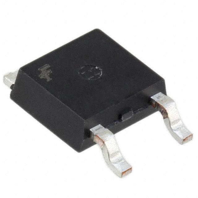
| 产品图片 |
|
| rohs | 符合RoHS无铅 / 符合限制有害物质指令(RoHS)规范要求 |
| 产品系列 | 电源管理 IC,线性稳压器,Fairchild Semiconductor KA7915ATU- |
| 数据手册 | |
| 产品型号 | KA7915ATU |
| PCN设计/规格 | |
| PSRR/纹波抑制—典型值 | 60 dB |
| 产品种类 | |
| 供应商器件封装 | TO-220-3 |
| 包装 | 管件 |
| 单位重量 | 1.800 g |
| 商标 | Fairchild Semiconductor |
| 安装类型 | 通孔 |
| 安装风格 | Through Hole |
| 封装 | Tube |
| 封装/外壳 | TO-220-3 |
| 封装/箱体 | TO-220-3 |
| 工作温度 | 0°C ~ 125°C |
| 工厂包装数量 | 50 |
| 最大工作温度 | + 125 C |
| 最大输入电压 | - 30 V |
| 最小工作温度 | 0 C |
| 最小输入电压 | - 17.5 V |
| 极性 | Negative |
| 标准包装 | 50 |
| 电压-跌落(典型值) | 2V @ 1A |
| 电压-输入 | 可下调至 -35V |
| 电压-输出 | -15V |
| 电流-输出 | 1A |
| 电流-限制(最小值) | - |
| 稳压器拓扑 | 负,固定式 |
| 稳压器数 | 1 |
| 系列 | KA7915 |
| 线路调整率 | 150 mV |
| 负载调节 | 150 mV |
| 输出电压 | - 15 V |
| 输出电流 | 1 A |
| 输出端数量 | 1 |
| 输出类型 | Fixed |


- 商务部:美国ITC正式对集成电路等产品启动337调查
- 曝三星4nm工艺存在良率问题 高通将骁龙8 Gen1或转产台积电
- 太阳诱电将投资9.5亿元在常州建新厂生产MLCC 预计2023年完工
- 英特尔发布欧洲新工厂建设计划 深化IDM 2.0 战略
- 台积电先进制程称霸业界 有大客户加持明年业绩稳了
- 达到5530亿美元!SIA预计今年全球半导体销售额将创下新高
- 英特尔拟将自动驾驶子公司Mobileye上市 估值或超500亿美元
- 三星加码芯片和SET,合并消费电子和移动部门,撤换高东真等 CEO
- 三星电子宣布重大人事变动 还合并消费电子和移动部门
- 海关总署:前11个月进口集成电路产品价值2.52万亿元 增长14.8%


PDF Datasheet 数据手册内容提取
Is Now Part of To learn more about ON Semiconductor, please visit our website at www.onsemi.com Please note: As part of the Fairchild Semiconductor integration, some of the Fairchild orderable part numbers will need to change in order to meet ON Semiconductor’s system requirements. Since the ON Semiconductor product management systems do not have the ability to manage part nomenclature that utilizes an underscore (_), the underscore (_) in the Fairchild part numbers will be changed to a dash (-). This document may contain device numbers with an underscore (_). Please check the ON Semiconductor website to verify the updated device numbers. The most current and up-to-date ordering information can be found at www.onsemi.com. Please email any questions regarding the system integration to Fairchild_questions@onsemi.com. ON Semiconductor and the ON Semiconductor logo are trademarks of Semiconductor Components Industries, LLC dba ON Semiconductor or its subsidiaries in the United States and/or other countries. ON Semiconductor owns the rights to a number of patents, trademarks, copyrights, trade secrets, and other intellectual property. A listing of ON Semiconductor’s product/patent coverage may be accessed at www.onsemi.com/site/pdf/Patent-Marking.pdf. ON Semiconductor reserves the right to make changes without further notice to any products herein. ON Semiconductor makes no warranty, representation or guarantee regarding the suitability of its products for any particular purpose, nor does ON Semiconductor assume any liability arising out of the application or use of any product or circuit, and specifically disclaims any and all liability, including without limitation special, consequential or incidental damages. Buyer is responsible for its products and applications using ON Semiconductor products, including compliance with all laws, regulations and safety requirements or standards, regardless of any support or applications information provided by ON Semiconductor. “Typical” parameters which may be provided in ON Semiconductor data sheets and/or specifications can and do vary in different applications and actual performance may vary over time. All operating parameters, including “Typicals” must be validated for each customer application by customer’s technical experts. ON Semiconductor does not convey any license under its patent rights nor the rights of others. ON Semiconductor products are not designed, intended, or authorized for use as a critical component in life support systems or any FDA Class 3 medical devices or medical devices with a same or similar classification in a foreign jurisdiction or any devices intended for implantation in the human body. Should Buyer purchase or use ON Semiconductor products for any such unintended or unauthorized application, Buyer shall indemnify and hold ON Semiconductor and its officers, employees, subsidiaries, affiliates, and distributors harmless against all claims, costs, damages, and expenses, and reasonable attorney fees arising out of, directly or indirectly, any claim of personal injury or death associated with such unintended or unauthorized use, even if such claim alleges that ON Semiconductor was negligent regarding the design or manufacture of the part. ON Semiconductor is an Equal Opportunity/Affirmative Action Employer. This literature is subject to all applicable copyright laws and is not for resale in any manner.
K A 7 9 September 2014 X X / K A KA79XX / KA79XXA / LM79XX 7 9 X 3-Terminal 1 A Negative Voltage Regulator X A / L M 7 9 Features Description X X • Output Current in Excess of 1 A The KA79XX / KA79XXA / LM79XX series of three-termi- — • Output Voltages of: -5 V, -6 V, -8 V, -9 V, -12 V, -15 V, nal negative regulators are available in a TO-220 pack- age with several fixed output voltages, making them 3 -18 V, -24 V - useful in a wide range of applications. Each type employs T • Internal Thermal Overload Protection e internal current limiting, thermal shutdown, and safe r • Short-Circuit Protection m operating area protection. i • Output Transistor Safe Operating Area Compensation n a TO-220 l 1 Input A N e g a t 1 iv e 1. GND 2. Input 3. Output V o l t a g Ordering Information e R e Output Voltage Operating g Product Number Package Packing Method Tolerance Temperature u l a KA7905TU to r KA7906TU KA7908TU KA7909TU ±4% KA7912TU TO-220 KA7915TU (Dual Gauge) KA7918TU KA7924TU KA7912ATU Rail 0 to +125°C ±2% KA7915ATU LM7905CT LM7908CT LM7909CT TO-220 LM7910CT ±4% (Single Gauge) LM7912CT LM7915CT LM7918CT © 2002 Fairchild Semiconductor Corporation www.fairchildsemi.com KA79XX / KA79XXA / LM79XX Rev. 1.1.1
K A Block Diagram 7 9 X X GND / K R1 A 7 9 VOLTAGE X REFERENCE R2 X A OOuutptut / + L M Q1 7 - 9 Q2 X X PROTECTION — I1 I2 CIRCUITRY 3 - Rsc T e r m In i Input n a l 1 Figure 1. Block Diagram A N e g Absolute Maximum Ratings a t i v Stresses exceeding the absolute maximum ratings may damage the device. The device may not function or be opera- e ble above the recommended operating conditions and stressing the parts to these levels is not recommended. In addi- V o tion, extended exposure to stresses above the recommended operating conditions may affect device reliability. The l t absolute maximum ratings are stress ratings only. Values are at T = 25°C unless otherwise noted. a A g e Symbol Parameter Value Unit R e VI Input Voltage -35 V g RθJC Thermal Resistance, Junction-Case(1) 5 °C/W ula RθJA Thermal Resistance, Junction-Air(1, 2) 65 °C/W to r T Operating Temperature Range 0 to +125 °C OPR T Storage Temperature Range - 65 to +150 °C STG Notes: 1. Thermal resistance test board, size: 76.2 mm x 114.3 mm x 1.6 mm(1S0P), JEDEC standard: JESD51-3, JESD51-7. 2. Assume no ambient airflow. © 2002 Fairchild Semiconductor Corporation www.fairchildsemi.com KA79XX / KA79XXA / LM79XX Rev. 1.1.1 2
K A Electrical Characteristics (KA7905 / LM7905) 7 9 (V = -10 V, I = 500 mA, 0°C ≤ T ≤ +125°C, C = 2.2 μF, C = 1 μF; unless otherwise specified.) X I O J I O X Symbol Parameter Conditions Min. Typ. Max. Unit / K T = +25°C -4.80 -5.00 -5.20 A J 7 VO Output Voltage IO = 5 mA to 1 A, PO ≤ 15 W, -4.75 -5.00 -5.25 V 9X V = -7 V to -20 V X I A ΔVO Line Regulation(3) TJ = +25°C VVI == --87 VV ttoo --1225 VV 385 15000 mV / L I M T = +25°C, I = 5 mA to 1.5 A 10 100 7 ΔV Load Regulation(3) J O mV 9 O T = +25°C, I = 250 mA to 750 mA 3 50 X J O X IQ Quiescent Current TJ = +25°C 3 6 mA — ΔIQ QChuaiensgceent Current IVO == -58 m VA t oto - 215 A V 00..1005 00..8500 mA 3-T I e r ΔVo/ΔT Temperature Coefficient I = 5 mA -0.4 mV/°C m of V O i D n VN Output Noise Voltage f = 10 Hz to 100 kHz, TA = +25°C 40 μV al 1 RR Ripple Rejection f = 120 Hz, ΔVI = 10 V 54 60 dB A VD Dropout Voltage TJ = +25°C, IO = 1 A 2 V N ISC Short-Circuit Current TJ = +25°C, VI = -35 V 300 mA eg a IPK Peak Current TJ = +25°C 2.2 A ti v e Note: V 3. Load and line regulation are specified at constant junction temperature. Changes in V due to heating effects must o O l be taken into account separately. Pulse testing with low duty is used. ta g e R e g u l a t o r © 2002 Fairchild Semiconductor Corporation www.fairchildsemi.com KA79XX / KA79XXA / LM79XX Rev. 1.1.1 3
K A Electrical Characteristics (KA7906) 7 9 (V = -11 V, I = 500 mA, 0°C ≤ T ≤ +125°C, C = 2.2 μF, C = 1 μF; unless otherwise specified.) X I O J I O X Symbol Parameter Conditions Min. Typ. Max. Unit / K T = +25°C -5.75 -6.00 -6.25 A J 7 VO Output Voltage IO = 5 mA to 1 A, PO ≤ 15 W, -5.70 -6.00 -6.30 V 9X V = -9 V to -21 V X I A ΔVO Line Regulation(4) TJ = +25°C VVI == --98 VV ttoo --1235 VV 150 16200 mV / L I M T = +25°C, I = 5 mA to 1.5 A 10 120 7 ΔV Load Regulation(4) J O mV 9 O T = +25°C, I = 250 mA to 750 mA 3 60 X J O X IQ Quiescent Current TJ = +25°C 3 6 mA — ΔIQ QChuaiensgceent Current IVO == -58 m VA t oto - 215 A V 00..1005 10..3500 mA 3-T I e r ΔVo/ΔT Temperature Coefficient I = 5 mA -0.5 mV/°C m of V O i D n VN Output Noise Voltage f = 10 Hz to 100 kHz, TA =+25°C 130 μV al 1 RR Ripple Rejection f = 120 Hz, ΔVI = 10 V 54 60 dB A VD Dropout Voltage TJ = +25°C, IO = 1 A 2 V N ISC Short-Circuit Current TJ = +25°C, VI = -35 V 300 mA eg a IPK Peak Current TJ = +25°C 2.2 A ti v e Note: V 4. Load and line regulation are specified at constant junction temperature. Changes in V due to heating effects must o O l be taken into account separately. Pulse testing with low duty is used. ta g e R e g u l a t o r © 2002 Fairchild Semiconductor Corporation www.fairchildsemi.com KA79XX / KA79XXA / LM79XX Rev. 1.1.1 4
K A Electrical Characteristics (KA7908 / LM7908) 7 9 (V = -14 V, I = 500 mA, 0°C ≤ T ≤ +125°C, C = 2.2 μF, C =1 μF; unless otherwise specified.) X I O J I O X Symbol Parameter Conditions Min. Typ. Max. Unit / K T = +25°C -7.7 -8.0 -8.3 A J 7 VO Output Voltage IO = 5 mA to 1 A, PO ≤ 15 W, -7.6 -8.0 -8.4 V 9X V = -10 V to -23 V X I A ΔVO Line Regulation(5) TJ = +25°C VVI == --1101.5 V V t oto - -1275 VV 150 18600 mV / L I M T = +25°C, I = 5 mA to 1.5 A 12 160 7 ΔV Load Regulation(5) J O mV 9 O T = +25°C, I = 250 mA to 750 mA 4 80 X J O X IQ Quiescent Current TJ = +25°C 3 6 mA — ΔIQ QChuaiensgceent Current IVO == -51 m0.A5 Vto t1o A-25 V 00..0150 01..0500 mA 3-T I e r ΔVo/ΔT Temperature Coefficient I = 5 mA -0.6 mV/°C m of V O i D n VN Output Noise Voltage f = 10 Hz to 100 kHz, TA = +25°C 175 μV al 1 RR Ripple Rejection f = 120 Hz, ΔVI = 10 V 54 60 dB A VD Dropout Voltage TJ = +25°C, IO = 1 A 2 V N ISC Short-Circuit Current TJ = +25°C, VI = -35 V 300 mA eg a IPK Peak Current TJ = +25°C 2.2 A ti v e Note: V 5. Load and line regulation are specified at constant junction temperature. Changes in V due to heating effects must o O l be taken into account separately. Pulse testing with low duty is used. ta g e R e g u l a t o r © 2002 Fairchild Semiconductor Corporation www.fairchildsemi.com KA79XX / KA79XXA / LM79XX Rev. 1.1.1 5
K A Electrical Characteristics (KA7909 / LM7909) 7 9 (V = -15 V, I = 500 mA, 0°C ≤ T ≤ +125°C, C = 2.2 μF, C =1 μF; unless otherwise specified.) X I O J I O X Symbol Parameter Conditions Min. Typ. Max. Unit / K T = +25°C -8.7 -9.0 -9.3 A J 7 VO Output Voltage IO = 5 mA to 1 A, PO ≤ 15 W, -8.6 -9.0 -9.4 V 9X V = -1.5 V to -23 V X I A ΔVO Line Regulation(6) TJ = +25°C VVI == --1121 .V5 Vto t-o1 8-2 V6 V 150 19800 mV / L I M T = +25°C, I = 5 mA to 1.5 A 12 180 7 ΔV Load Regulation(6) J O mV 9 O T = +25°C, I = 250 mA to 750 mA 4 90 X J O X IQ Quiescent Current TJ = +25°C 3 6 mA — ΔIQ QChuaiensgceent Current IVO == -51 m1.A5 Vto t1o A-26 V 00..1005 10..0500 mA 3-T I e r ΔVo/ΔT Temperature Coefficient I = 5 mA -0.6 mV/°C m of V O i D n VN Output Noise Voltage f = 10 Hz to 100 kHz, TA = +25°C 175 μV al 1 RR Ripple Rejection f = 120 Hz, ΔVI = 10 V 54 60 dB A VD Dropout Voltage TJ = +25°C, IO = 1 A 2 V N ISC Short-Circuit Current TJ = +25°C, VI = -35 V 300 mA eg a IPK Peak Current TJ = +25°C 2.2 A ti v e Note: V 6. Load and line regulation are specified at constant junction temperature. Changes in V due to heating effects must o O l be taken into account separately. Pulse testing with low duty is used. ta g e R e g u l a t o r © 2002 Fairchild Semiconductor Corporation www.fairchildsemi.com KA79XX / KA79XXA / LM79XX Rev. 1.1.1 6
K A Electrical Characteristics (LM7910) 7 9 (V = -17 V, I = 500 mA, 0°C ≤ T ≤ +125°C, C = 2.2 μF, C =1 μF; unless otherwise specified.) X I O J I O X Symbol Parameter Conditions Min. Typ. Max. Unit / K T = +25°C -9.6 -10.0 -10.4 A J 7 VO Output Voltage IO = 5 mA to 1A, Pd ≤ 15 W, -9.5 -10.0 -10.5 V 9X V = -12 V to -28 V X I A ΔVO Line Regulation(7) TJ = +25°C VVI == --1142 .V5 Vto t-o2 0-2 V8 V 162 210000 mV / L I M T = +25°C, 7 J 12 200 9 ΔVO Load Regulation(7) ITOJ == 5+ 2m5A°C to, 1.5 A 4 100 mV XX — I = 250 mA to 750 mA O IQ Quiescent Current TJ = +25°C 3 6 mA 3-T ΔIQ QChuaiensgceent Current IVO == -51 m2.A5 Vto t1o A-28 V 00..1005 10..0500 mA erm I i n Temperature Coefficient a ΔVo/ΔT of VO IO = 5 mA -1 mV/°C l 1 V Output Noise Voltage 10 Hz ≤ f ≤ 100 kHz, T = +25°C 280 μV A N A N RR Ripple Rejection f = 120 Hz, ΔV = 10 V 54 60 dB I e g VD Dropout Voltage TJ = +25°C, IO = 1 A 2 V a t ISC Short-Circuit Current TJ = +25°C, VI = -35 V 300 mA iv e IPK Peak Current TJ = +25°C 2.2 A V o Note: lt a 7. Load and line regulation are specified at constant junction temperature. Changes in V due to heating effects must g O e be taken into account separately. Pulse testing with low duty is used. R e g u l a t o r © 2002 Fairchild Semiconductor Corporation www.fairchildsemi.com KA79XX / KA79XXA / LM79XX Rev. 1.1.1 7
K A Electrical Characteristics (KA7912 / LM7912) 7 9 (V = -19 V, I = 500 mA, 0°C ≤ T ≤ +125°C, C = 2.2 μF, C = 1 μF; unless otherwise specified.) X I O J I O X Symbol Parameter Conditions Min. Typ. Max. Unit / K T = +25°C -11.5 -12.0 -12.5 A J 7 VO Output Voltage IO = 5 mA to 1 A, PO ≤ 15 W -11.4 -12.0 -12.6 V 9X V = -15.5 V to -27 V X I A ΔVO Line Regulation(8) TJ = +25°C VVI == --1164 .V5 Vto t-o2 -23 V0 V 162 122400 mV / L I M T = +25°C, I = 5 mA to 1.5 A 12 240 7 ΔV Load Regulation(8) J O mV 9 O T = +25°C, I = 250 mA to 750 mA 4 120 X J O X IQ Quiescent Current TJ = +25°C 3 6 mA — ΔIQ QChuaiensgceent Current IVO == -51 m4.A5 Vto t1o A-30 V 00..1005 10..0500 mA 3-T I e r ΔVo/ΔT Temperature Coefficient I = 5 mA -0.8 mV/°C m of V O i D n VN Output Noise Voltage f = 10 Hz to 100 kHz, TA = +25°C 200 μV al 1 RR Ripple Rejection f = 120 Hz, ΔVI = 10 V 54 60 dB A VD Dropout Voltage TJ = +25°C, IO = 1 A 2 V N ISC Short-Circuit Current TJ = +25°C, VI = -35 V 300 mA eg a IPK Peak Current TJ = +25°C 2.2 A ti v e Note: V 8. Load and line regulation are specified at constant junction temperature. Changes in V due to heating effects must o O l be taken into account separately. Pulse testing with low duty is used. ta g e R e g u l a t o r © 2002 Fairchild Semiconductor Corporation www.fairchildsemi.com KA79XX / KA79XXA / LM79XX Rev. 1.1.1 8
K A Electrical Characteristics (KA7915 / LM7915) 7 9 (V = -23 V, I = 500 mA, 0°C ≤T ≤ +125°C, C = 2.2 μF, C = 1 μF; unless otherwise specified.) X I O J I O X Symbol Parameter Conditions Min. Typ. Max. Unit / K T = +25°C -14.40 -15.00 -15.60 A J 7 VO Output Voltage IO = 5 mA to 1 A, PO ≤ 15 W -14.25 -15.00 -15.75 V 9X V = -18 V to -30 V X I A ΔVO Line Regulation(9) TJ = +25°C VVI == --2107 .V5 Vto t-o2 -63 V0 V 162 310500 mV / L I M T = +25°C, I = 5 mA to 1.5 A 12 300 7 ΔV Load Regulation(9) J O mV 9 O T = +25°C, I = 250 mA to 750 mA 4 150 X J O X IQ Quiescent Current TJ = +25°C 3 6 mA — ΔIQ QChuaiensgceent Current IVO == -51 m7.A5 Vto t1o A-30 V 00..1005 10..0500 mA 3-T I e r ΔVo/ΔT Temperature Coefficient I = 5 mA -0.9 mV/°C m of V O i D n VN Output Noise Voltage f = 10 Hz to 100 kHz, TA = +25°C 250 μV al 1 RR Ripple Rejection f = 120 Hz, ΔVI = 10 V 54 60 dB A VD Dropout Voltage TJ = +25°C, IO = 1 A 2 V N ISC Short-Circuit Current TJ = +25°C, VI = -35 V 300 mA eg a IPK Peak Current TJ = +25°C 2.2 A ti v e Note: V 9. Load and line regulation are specified at constant junction temperature. Changes in V due to heating effects must o O l be taken into account separately. Pulse testing with low duty is used. ta g e R e g u l a t o r © 2002 Fairchild Semiconductor Corporation www.fairchildsemi.com KA79XX / KA79XXA / LM79XX Rev. 1.1.1 9
K A Electrical Characteristics (KA7918 / LM7918) 7 9 (V = -27 V, I = 500 mA, 0°C ≤ T ≤ +125°C, C = 2.2 μF, C =1 μF, unless otherwise specified.) X I O J I O X Symbol Parameter Conditions Min. Typ. Max. Unit / K T = +25°C -17.3 -18.0 -18.7 A J 7 VO Output Voltage IO = 5 mA to 1 A, PO ≤ 15 W -17.1 -18.0 -18.9 V 9X V = -22.5 V to -33 V X I A ΔVO Line Regulation(10) TJ = +25°C VVI == --2214 VV ttoo --3330 VV 185 316800 mV / L I M T = +25°C, I = 5 mA to 1.5 A 15 360 7 ΔV Load Regulation(10) J O mV 9 O T = +25°C, I = 250 mA to 750 mA 5 180 X J O X IQ Quiescent Current TJ = +25°C 3 6 mA — ΔIQ QChuaiensgceent Current IVO == -52 m1 AV ttoo 1-3 A3 V 00..1005 10..0500 mA 3-T I e r ΔVo/ΔT Temperature Coefficient I = 5 mA -1 mV/°C m of V O i D n VN Output Noise Voltage f = 10 Hz to 100 kHz, TA = +25°C 300 μV al 1 RR Ripple Rejection f = 120 Hz, ΔVI = 10 V 54 60 dB A VD Dropout Voltage TJ = +25°C, IO = 1 A 2 V N ISC Short-Circuit Current TJ = +25°C, VI = -35 V 300 mA eg a IPK Peak Current TJ = +25°C 2.2 A ti v e Note: V 10. Load and line regulation are specified at constant junction temperature. Changes in V due to heating effects must o O l be taken into account separately. Pulse testing with low duty is used. ta g e R e g u l a t o r © 2002 Fairchild Semiconductor Corporation www.fairchildsemi.com KA79XX / KA79XXA / LM79XX Rev. 1.1.1 10
K A Electrical Characteristics (KA7924) 7 9 (V = -33 V, I = 500 mA, 0°C ≤ T ≤ +125°C, C = 2.2 μF, C = 1 μF; unless otherwise specified.) X I O J I O X Symbol Parameter Conditions Min. Typ. Max. Unit / K T = +25°C -23.0 -24.0 -25.0 A J 7 VO Output Voltage IO = 5 mA to 1 A, PO ≤ 15 W, -22.8 -24.0 -25.2 V 9X V = -27 V to -38 V X I A ΔVO Line Regulation(11) TJ = +25°C VVI == --3207 VV ttoo --3368 VV 185 148800 mV / L I M T = +25°C, I = 5 mA to 1.5 A 15 480 7 ΔV Load Regulation(11) J O mV 9 O T = +25°C, I = 250 mA to 750 mA 5 240 X J O X IQ Quiescent Current TJ = +25°C 3 6 mA — ΔIQ QChuaiensgceent Current IVO == -52 m7 AV ttoo 1-3 A8 V 00..1005 10..0500 mA 3-T I e r ΔVo/ΔT Temperature Coefficient I = 5 mA -1 mV/°C m of V O i D n VN Output Noise Voltage f = 10 Hz to 100 kHz, TA = +25°C 400 μV al 1 RR Ripple Rejection f = 120 Hz, ΔVI = 10 V 54 60 dB A VD Dropout Voltage TJ = +25°C, IO = 1 A 2 V N ISC Short-Circuit Current TJ = +25°C, VI = -35 V 300 mA eg a IPK Peak Current TJ = +25°C 2.2 A ti v e Note: V 11. Load and line regulation are specified at constant junction temperature. Changes in V due to heating effects must o O l be taken into account separately. Pulse testing with low duty is used. ta g e R e g u l a t o r © 2002 Fairchild Semiconductor Corporation www.fairchildsemi.com KA79XX / KA79XXA / LM79XX Rev. 1.1.1 11
K A Electrical Characteristics (KA7912A) 7 9 (V = -19 V, I = 500 mA, 0°C ≤ T ≤ +125°C, C = 2.2 μF, C =1 μF; unless otherwise specified.) X I O J I O X Symbol Parameter Conditions Min. Typ. Max. Unit / K T = +25°C -11.75 -12.00 -12.25 A J 7 VO Output Voltage IO = 5 mA to 1 A, PO ≤ 15 W, -11.50 -12.00 -12.50 V 9X V = -15.5 V to -27 V X I A VI = -14.5 V to -27 V, 12 120 / Io = 1 A L TJ = +25°C M V= -16 V to -22 V, ΔVO Line Regulation(12) IoI = 1 A 6 60 mV 79 X V = -14.8 V to -30 V 12 120 X I — V = -16 V to -22 V, Io = 1 A 12 120 I ΔV Load Regulation(12) TJ = +25°C, IO = 5 mA to 1.5 A 12 150 mV 3-T O T = +25°C, I = 250 mA to 750 mA 4 75 e J O r m I Quiescent Current T = +25°C 3 6 mA Q J i n ΔIQ QChuaiensgceent Current IVO == -51 m5 AV ttoo 1-3 A0 V 00..1005 10..0500 mA al 1 I A ΔVo/ΔT Temperature Coefficient I = 5 mA -0.8 mV/°C N of V O D e g VN Output Noise Voltage f = 10 Hz to 100 kHz, TA = +25°C 200 μV a t RR Ripple Rejection f = 120 Hz, ΔVI = 10 V 54 60 dB iv e VD Dropout Voltage TJ = +25°C, IO = 1 A 2 V V o ISC Short-Circuit Current TJ = +25°C, VI = -35 V 300 mA lt a IPK Peak Current TJ = +25°C 2.2 A g e Note: R e 12. Load and line regulation are specified at constant junction temperature. Changes in VO due to heating effects must g u be taken into account separately. Pulse testing with low duty is used. l a t o r © 2002 Fairchild Semiconductor Corporation www.fairchildsemi.com KA79XX / KA79XXA / LM79XX Rev. 1.1.1 12
K A Electrical Characteristics (KA7915A) 7 9 (V = -23 V, I = 500 mA, 0°C ≤ T ≤ +125°C, C = 2.2 μF, C = 1 μF; unless otherwise specified.) X I O J I O X Symbol Parameter Conditions Min. Typ. Max. Unit / K T = +25°C -14.7 -15.0 -15.3 A J 7 VO Output Voltage IO = 5 mA to 1 A, PO ≤ 15 W, -14.4 -15.0 -15.6 V 9X V = -18 V to -30 V X I A VI = -17.5 V to -30 V, 12 150 / Io = 1 A L TJ = +25°C M V = -20 V to -26 V, ΔVO Line Regulation(13) IoI = 1 A 6 75 mV 79 X V = -17.9 V to -30 V 12 150 X I — V = -20 V to -26 V, Io = 1 A 6 150 I ΔV Load Regulation(13) TJ = +25°C, IO = 5 mA to 1.5 A 12 150 mV 3-T O T = +25°C, I = 250 mA to 750 mA 4 75 e J O r m I Quiescent Current T = +25°C 3 6 mA Q J i n ΔIQ QChuaiensgceent Current IVO == -51 m8.A5 Vto t1o A-30 V 00..1005 10..0500 mA al 1 I A ΔVo/ΔT Temperature Coefficient I = 5 mA -0.9 mV/°C N of V O D e g VN Output Noise Voltage f = 10 Hz to 100 kHz, TA = +25°C 250 μV a t RR Ripple Rejection f = 120 Hz, ΔVI = 10 V 54 60 dB iv e VD Dropout Voltage TJ = +25°C, IO = 1 A 2 V V o ISC Short-Circuit Current TJ = +25°C, VI = -35 V 300 mA lt a IPK Peak Current TJ = +25°C 2.2 A g e Note: R e 13. Load and line regulation are specified at constant junction temperature. Changes in VO due to heating effects must g u be taken into account separately. Pulse testing with low duty is used. l a t o r © 2002 Fairchild Semiconductor Corporation www.fairchildsemi.com KA79XX / KA79XXA / LM79XX Rev. 1.1.1 13
K A Typical Performance Characteristics 7 9 X X / K A 5.1 15 7 OV]u5.05 VIoi=n=401m0VA V] Lo13 Io=1.5A 9X tuge[-pt 5 n[m aRde119 XA VlVoltatao4.95 atio gatuil 57 / L g[Vutput -e] 4.9 VIoi=n=10205mVA Regul o[Vmn] 13 Io=0.75A M79 O 4.85 d -1 X a -3 X 4.8 Lo -5 — -40 -25 0 25 50 75 100 125 25 -40 -25 0 25 50 75 100 125 TA, Ambient Temperature [oC] TA, Ambient Temperature [oC] 3- T e r m Figure 2. Output Voltage Figure 3. Load Regulation i n a l 1 A N 5 4 e g A]4.5 3.5 a uiescent Current [m123...1234555 DVl[V] Dropout Voltage [V]12..55123 Io=1A tive Voltage Q0.5 0.5 R 0 0 e -40 -25 0 25 50 75 100 125 5 -40 -25 0 25 50 75 100 125 g TA, Ambient Temperature [oC] TA, Ambient Temperature [oC] ul a t o r Figure 4. Quiescent Current Figure 5. Dropout Voltage 0.6 0.55 Sh ent[A]oCritr0.004..545 urrcui0.35 Ct 0.3 uit Cu0.25 c 0.2 Cirrre0.15 hort n[At]0.00.51 S 0 -0.05 -0.1 -40 -25 0 25 50 75 100 125 TA, Ambient Temperature [oC] Figure 6. Short-Circuit Current © 2002 Fairchild Semiconductor Corporation www.fairchildsemi.com KA79XX / KA79XXA / LM79XX Rev. 1.1.1 14
K A Typical Applications 7 9 X X / K A 7 2.2 μF + 1 μF 9X + X C Co A I 1 / L 2 KA79XX 3 M Input LM79XX Output 7 9 X X — 3 Figure 7. Negative Fixed Output Regulator -T e r m i n a l 1 +15 V 1 KA7812 3 +12 V A LM7812 N + 2 Co+ eg C1 0.33 μF 1N4001 a 1 μF * ti v e GND V o + 2.2 μF 1 μF+ lt a C1 Co 1N4001 g 1 * e R -15 V 2 KLMA77991122 3 -12 V eg u l a t o r Figure 8. Split Power Supply (±12 V / 1 A) Notes: 14.To specify an output voltage, substitute voltage value for "XX". 15.C is required if the regulator is located an appreciable distance from the power supply filter. For value given, I capacitor must be solid tantalum. If aluminium electronics are used, at least ten times the value shown should be selected. 16. C improves stability and transient response. If large capacitors are used, a high-current diode from input to O output (1N4001 or similar) should be introduced to protect the device from momentary input short circuit. © 2002 Fairchild Semiconductor Corporation www.fairchildsemi.com KA79XX / KA79XXA / LM79XX Rev. 1.1.1 15
K A Physical Dimensions 7 9 X X / K A 7 9 X X A / L M 7 9 X X — 3 - T e r m i n a l 1 A N e g a t i v e V o l t a g e R e g u l a t o r Figure 9. TO-220, MOLDED, 3-LEAD, JEDEC VARIATION AB (ACTIVE) © 2002 Fairchild Semiconductor Corporation www.fairchildsemi.com KA79XX / KA79XXA / LM79XX Rev. 1.1.1 16
TRADEMARKS The following includes registered and unregistered trademarks and service marks, owned by Fairchild Semiconductor and/or its global subsidiaries, and is not intended to be an exhaustive list of all such trademarks. AccuPower(cid:165) F-PFS(cid:165) Awinda® FRFET® ® ®* AX-CAP®* Global Power ResourceSM PowerTrench® TinyBoost® BitSiC(cid:165) GreenBridge(cid:165) PowerXS™ TinyBuck® Build it Now(cid:165) Green FPS(cid:165) Programmable Active Droop(cid:165) TinyCalc(cid:165) CorePLUS(cid:165) Green FPS(cid:165) e-Series(cid:165) QFET® TinyLogic® CorePOWER(cid:165) Gmax(cid:165) QS(cid:165) TINYOPTO(cid:165) CROSSVOLT(cid:165) GTO(cid:165) Quiet Series(cid:165) TinyPower(cid:165) CTL(cid:165) IntelliMAX(cid:165) RapidConfigure(cid:165) TinyPWM(cid:165) Current Transfer Logic(cid:165) ISOPLANAR(cid:165) (cid:165) TinyWire(cid:165) DEUXPEED® Making Small Speakers Sound Louder TranSiC(cid:165) Dual Cool™ and Better™ Saving our world, 1mW/W/kW at a time™ TriFault Detect(cid:165) EcoSPARK® MegaBuck(cid:165) SignalWise(cid:165) TRUECURRENT®* EfficientMax(cid:165) MICROCOUPLER(cid:165) SmartMax(cid:165) μSerDes(cid:165) ESBC(cid:165) MicroFET(cid:165) SMART START(cid:165) Fairch®ild® MMiiccrrooPPaakk2(cid:165)(cid:165) SSSToPlEMuAt®ioLnTsH f(cid:165)or Your Success(cid:165) UHC® Fairchild Semiconductor® MillerDrive(cid:165) SuperFET® Ultra FRFET(cid:165) MotionMax(cid:165) UniFET(cid:165) FFFFFAEAAasCTCStBTvTTC®e® Qnocurehie(cid:165)(cid:165)t Series(cid:165) MMMMmTToVWtixN®iS®o®naGverird®® SSSSSuuuuynppppecreeerFrrSMSSEOOOTOT(cid:165)TTS(cid:165)(cid:165)(cid:165)®-3--68 XVVVXsCioSsel™Xutnaa(cid:165)sg l™MePalxu(cid:165)s(cid:165) FPS(cid:165) Sync-Lock™ OptoHiT(cid:165) (cid:3037)(cid:10106)™ * Trademarks of System General Corporation, used under license by Fairchild Semiconductor. DISCLAIMER FAIRCHILD SEMICONDUCTOR RESERVES THE RIGHT TO MAKE CHANGES WITHOUT FURTHER NOTICE TO ANY PRODUCTS HEREIN TO IMPROVE RELIABILITY, FUNCTION, OR DESIGN. TO OBTAIN THE LATEST, MOST UP-TO-DATE DATASHEET AND PRODUCT INFORMATION, VISIT OUR WEBSITE AT HTTP://WWW.FAIRCHILDSEMI.COM.FAIRCHILD DOES NOT ASSUME ANY LIABILITY ARISING OUT OF THE APPLICATION OR USE OF ANY PRODUCT OR CIRCUIT DESCRIBED HEREIN; NEITHER DOES IT CONVEY ANY LICENSE UNDER ITS PATENT RIGHTS, NOR THE RIGHTS OF OTHERS. THESE SPECIFICATIONS DO NOT EXPAND THE TERMS OF FAIRCHILD’S WORLDWIDE TERMS AND CONDITIONS, SPECIFICALLY THE WARRANTY THEREIN, WHICH COVERS THESE PRODUCTS. LIFE SUPPORT POLICY FAIRCHILD’S PRODUCTS ARE NOT AUTHORIZED FOR USE AS CRITICAL COMPONENTS IN LIFE SUPPORT DEVICES OR SYSTEMS WITHOUT THE EXPRESS WRITTEN APPROVAL OF FAIRCHILD SEMICONDUCTOR CORPORATION. As used herein: 1. Life support devices or systems are devices or systems which, (a) are 2. A critical component in any component of a life support, device, or intended for surgical implant into the body or (b) support or sustain system whose failure to perform can be reasonably expected to life, and (c) whose failure to perform when properly used in cause the failure of the life support device or system, or to affect its accordance with instructions for use provided in the labeling, can be safety or effectiveness. reasonably expected to result in a significant injury of the user. ANTI-COUNTERFEITING POLICY Fairchild Semiconductor Corporation's Anti-Counterfeiting Policy. Fairchild's Anti-Counterfeiting Policy is also stated on our external website, www.fairchildsemi.com, under Sales Support. Counterfeiting of semiconductor parts is a growing problem in the industry. All manufacturers of semiconductor products are experiencing counterfeiting of their parts. Customers who inadvertently purchase counterfeit parts experience many problems such as loss of brand reputation, substandard performance, failed applications, and increased cost of production and manufacturing delays. Fairchild is taking strong measures to protect ourselves and our customers from the proliferation of counterfeit parts. Fairchild strongly encourages customers to purchase Fairchild parts either directly from Fairchild or from Authorized Fairchild Distributors who are listed by country on our web page cited above. Products customers buy either from Fairchild directly or from Authorized Fairchild Distributors are genuine parts, have full traceability, meet Fairchild's quality standards for handling and storage and provide access to Fairchild's full range of up-to-date technical and product information. Fairchild and our Authorized Distributors will stand behind all warranties and will appropriately address any warranty issues that may arise. Fairchild will not provide any warranty coverage or other assistance for parts bought from Unauthorized Sources. Fairchild is committed to combat this global problem and encourage our customers to do their part in stopping this practice by buying direct or from authorized distributors. PRODUCT STATUS DEFINITIONS Definition of Terms Datasheet Identification Product Status Definition Datasheet contains the design specifications for product development. Specifications may change Advance Information Formative / In Design in any manner without notice. Datasheet contains preliminary data; supplementary data will be published at a later date. Fairchild Preliminary First Production Semiconductor reserves the right to make changes at any time without notice to improve design. Datasheet contains final specifications. Fairchild Semiconductor reserves the right to make No Identification Needed Full Production changes at any time without notice to improve the design. Datasheet contains specifications on a product that is discontinued by Fairchild Semiconductor. Obsolete Not In Production The datasheet is for reference information only. Rev. I71 © Fairchild Semiconductor Corporation www.fairchildsemi.com
ON Semiconductor and are trademarks of Semiconductor Components Industries, LLC dba ON Semiconductor or its subsidiaries in the United States and/or other countries. ON Semiconductor owns the rights to a number of patents, trademarks, copyrights, trade secrets, and other intellectual property. A listing of ON Semiconductor’s product/patent coverage may be accessed at www.onsemi.com/site/pdf/Patent−Marking.pdf. ON Semiconductor reserves the right to make changes without further notice to any products herein. ON Semiconductor makes no warranty, representation or guarantee regarding the suitability of its products for any particular purpose, nor does ON Semiconductor assume any liability arising out of the application or use of any product or circuit, and specifically disclaims any and all liability, including without limitation special, consequential or incidental damages. Buyer is responsible for its products and applications using ON Semiconductor products, including compliance with all laws, regulations and safety requirements or standards, regardless of any support or applications information provided by ON Semiconductor. “Typical” parameters which may be provided in ON Semiconductor data sheets and/or specifications can and do vary in different applications and actual performance may vary over time. All operating parameters, including “Typicals” must be validated for each customer application by customer’s technical experts. ON Semiconductor does not convey any license under its patent rights nor the rights of others. ON Semiconductor products are not designed, intended, or authorized for use as a critical component in life support systems or any FDA Class 3 medical devices or medical devices with a same or similar classification in a foreign jurisdiction or any devices intended for implantation in the human body. Should Buyer purchase or use ON Semiconductor products for any such unintended or unauthorized application, Buyer shall indemnify and hold ON Semiconductor and its officers, employees, subsidiaries, affiliates, and distributors harmless against all claims, costs, damages, and expenses, and reasonable attorney fees arising out of, directly or indirectly, any claim of personal injury or death associated with such unintended or unauthorized use, even if such claim alleges that ON Semiconductor was negligent regarding the design or manufacture of the part. ON Semiconductor is an Equal Opportunity/Affirmative Action Employer. This literature is subject to all applicable copyright laws and is not for resale in any manner. PUBLICATION ORDERING INFORMATION LITERATURE FULFILLMENT: N. American Technical Support: 800−282−9855 Toll Free ON Semiconductor Website: www.onsemi.com Literature Distribution Center for ON Semiconductor USA/Canada 19521 E. 32nd Pkwy, Aurora, Colorado 80011 USA Europe, Middle East and Africa Technical Support: Order Literature: http://www.onsemi.com/orderlit Phone: 303−675−2175 or 800−344−3860 Toll Free USA/Canada Phone: 421 33 790 2910 Fax: 303−675−2176 or 800−344−3867 Toll Free USA/Canada Japan Customer Focus Center For additional information, please contact your local Email: orderlit@onsemi.com Phone: 81−3−5817−1050 Sales Representative © Semiconductor Components Industries, LLC www.onsemi.com www.onsemi.com 1
Mouser Electronics Authorized Distributor Click to View Pricing, Inventory, Delivery & Lifecycle Information: O N Semiconductor: KA7915ATU