ICGOO在线商城 > 集成电路(IC) > PMIC - 稳压器 - 线性 > TC2015-3.3VCTTR
 Datasheet下载
- 型号: TC2015-3.3VCTTR
- 制造商: Microchip
- 库位|库存: xxxx|xxxx
- 要求:
| 数量阶梯 | 香港交货 | 国内含税 |
| +xxxx | $xxxx | ¥xxxx |
查看当月历史价格
查看今年历史价格
TC2015-3.3VCTTR产品简介:
ICGOO电子元器件商城为您提供TC2015-3.3VCTTR由Microchip设计生产,在icgoo商城现货销售,并且可以通过原厂、代理商等渠道进行代购。 TC2015-3.3VCTTR价格参考。MicrochipTC2015-3.3VCTTR封装/规格:PMIC - 稳压器 - 线性, Linear Voltage Regulator IC 1 Output 100mA SOT-23-5。您可以下载TC2015-3.3VCTTR参考资料、Datasheet数据手册功能说明书,资料中有TC2015-3.3VCTTR 详细功能的应用电路图电压和使用方法及教程。
Microchip Technology的TC2015-3.3VCTTR是一款线性稳压器(LDO),属于电源管理集成电路(PMIC)的一部分。该器件专为提供高效、稳定的3.3V输出电压而设计,适用于对电源噪声敏感、要求高稳定性的应用场景。

其主要应用场景包括:

1. 便携式电子设备:如智能手机、平板电脑和手持仪器,TC2015具有低功耗和小型封装特点,适合电池供电系统中为处理器、传感器等模块提供稳定电源。

2. 嵌入式系统与工业控制:用于为微控制器(MCU)、FPGA、DSP等芯片提供干净电源,确保系统在复杂环境中稳定运行。

3. 通信设备:如无线基站、光模块和网络设备,TC2015可为射频(RF)电路和逻辑电路提供低噪声电源,减少干扰,提升信号完整性。

4. 传感器与测量仪器:在高精度数据采集系统中,作为参考电压源或为模拟前端供电,确保测量精度。

该器件具备快速瞬态响应、低静态电流和过热/过流保护功能,适合空间受限且对可靠性要求高的应用。其SOT-23封装也便于PCB布局和散热设计。
| 参数 | 数值 |
| 产品目录 | 集成电路 (IC)半导体 |
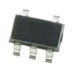
| 描述 | IC REG LDO 3.3V 0.1A SOT23-5低压差稳压器 .1mA w/Shtdn & Ref B 3.3V |
| 产品分类 | |
| 品牌 | Microchip Technology |
| 产品手册 | |
| 产品图片 |
|
| rohs | 符合RoHS无铅 / 符合限制有害物质指令(RoHS)规范要求 |
| 产品系列 | 电源管理 IC,低压差稳压器,Microchip Technology TC2015-3.3VCTTR- |
| 数据手册 | 点击此处下载产品Datasheethttp://www.microchip.com/mymicrochip/filehandler.aspx?ddocname=en011649http://www.microchip.com/mymicrochip/filehandler.aspx?ddocname=en023833 |
| 产品型号 | TC2015-3.3VCTTR |
| PSRR/纹波抑制—典型值 | 55 dB |
| 产品 | LDO Regulators |
| 产品种类 | 低压差稳压器 |
| 供应商器件封装 | SOT-23-5 |
| 其它名称 | TC20153.3VCTTR |
| 包装 | 带卷 (TR) |
| 商标 | Microchip Technology |
| 回动电压—最大值 | 140 mV |
| 安装类型 | 表面贴装 |
| 安装风格 | SMD/SMT |
| 封装 | Reel |
| 封装/外壳 | SC-74A,SOT-753 |
| 封装/箱体 | SOT-23A-5 |
| 工作温度 | -40°C ~ 125°C |
| 工厂包装数量 | 3000 |
| 最大功率耗散 | 0.318 W |
| 最大工作温度 | + 125 C |
| 最大输入电压 | 6 V |
| 最小工作温度 | - 40 C |
| 最小输入电压 | 2.7 V |
| 标准包装 | 3,000 |
| 电压-跌落(典型值) | 0.09V @ 100mA |
| 电压-输入 | 最高 6V |
| 电压-输出 | 3.3V |
| 电压调节准确度 | 0.4 % |
| 电流-输出 | 100mA |
| 电流-限制(最小值) | - |
| 电源电流 | 55 uA |
| 稳压器拓扑 | 正,固定式 |
| 稳压器数 | 1 |
| 类型 | LDO with Shutdown |
| 线路调整率 | 0.05 % |
| 负载调节 | 0.33 % |
| 输入偏压电流—最大 | 0.055 mA |
| 输出电压 | 3.3 V |
| 输出电流 | 100 mA |
| 输出端数量 | 1 Output |
| 输出类型 | Fixed |


- 商务部:美国ITC正式对集成电路等产品启动337调查
- 曝三星4nm工艺存在良率问题 高通将骁龙8 Gen1或转产台积电
- 太阳诱电将投资9.5亿元在常州建新厂生产MLCC 预计2023年完工
- 英特尔发布欧洲新工厂建设计划 深化IDM 2.0 战略
- 台积电先进制程称霸业界 有大客户加持明年业绩稳了
- 达到5530亿美元!SIA预计今年全球半导体销售额将创下新高
- 英特尔拟将自动驾驶子公司Mobileye上市 估值或超500亿美元
- 三星加码芯片和SET,合并消费电子和移动部门,撤换高东真等 CEO
- 三星电子宣布重大人事变动 还合并消费电子和移动部门
- 海关总署:前11个月进口集成电路产品价值2.52万亿元 增长14.8%


PDF Datasheet 数据手册内容提取
TC2014/2015/2185 50 mA, 100 mA, 150 mA CMOS LDOs with Shutdown and Reference Bypass Features General Description • Low Supply Current: 80µA (Max) The TC2014, TC2015 and TC2185 are high-accuracy • Low Dropout Voltage: 140mV (Typ.) @ 150mA (typically ±0.4%) CMOS upgrades for bipolar Low Drop-out Regulators (LDOs), such as the LP2980. • High-Output Voltage Accuracy: ±0.4% (Typ.) Total supply current is typically 55µA; 20 to 60 times • Standard or Custom Output Voltages lower than in bipolar regulators. • Power-Saving Shutdown Mode The key features of the device include low noise oper- • Reference Bypass Input for Ultra Low-Noise ation (plus bypass reference), low dropout voltage Operation –typically 45mV for the TC2014, 90mV for the • Fast Shutdown Response Time: 60µsec (Typ.) TC2015, and 140mV for the TC2185, at full load – and • Overcurrent and Overtemperature Protection fast response to step changes in load. Supply current • Space-Saving 5-Pin SOT-23A Package is reduced to 0.5µA (max) and VOUT falls to zero when the shutdown input is low. These devices also • Pin-Compatible Upgrades for Bipolar Regulators incorporate overcurrent and overtemperature • Wide Operating Temperature Range: protection. -40°C to +125°C The TC2014, TC2015 and TC2185 are stable with an • Standard Output Voltage Options: output capacitor of 1µF and have maximum output - 1.8V, 2.5V, 2.6V, 2.7V, 2.8V, 2.85V, 3.0V, currents of 50mA, 100mA and 150mA, respectively. 3.3V, 5.0V For higher-output current versions, see the TC1107 Applications (DS21356), TC1108 (DS21357) and TC1173 (DS21362) (I = 300mA) data sheets. OUT • Battery-Operated Systems • Portable Computers Typical Application • Medical Instruments • Instrumentation 1 5 • Cellular/GSM/PHS Phones VIN VIN VOUT VOUT • Linear Post-Regulator for SMPS + + 1µF 1µF • Pagers Related Literature 2 TC2014 • Application Notes: AN765, AN766, AN776 and GND TC2015 AN792 TC2185 Package Type 5-Pin SOT-23A 3 4 SHDN Bypass VOUT Bypass 0.01µF Reference 5 4 Bypass Cap (Optional) TC2014 Shutdown Control TC2015 (from Power Control Logic) TC2185 1 2 3 VIN GND SHDN © 2006 Microchip Technology Inc. DS21662E-page 1
TC2014/2015/2185 1.0 ELECTRICAL † Notice: Stresses above those listed under "Absolute CHARACTERISTICS Maximum Ratings" may cause permanent damage to the device. These are stress ratings only and functional operation of the device at these or any other conditions Absolute Maximum Ratings † above those indicated in the operation sections of the Input Voltage................................................................... 7.0V specifications is not implied. Exposure to Absolute Maximum Rating conditions for extended periods may Output Voltage....................................... (– 0.3) to (V + 0.3) IN affect device reliability. Operating Temperature......................... – 40°C < T < 125°C J Storage Temperature.................................. – 65°C to +150°C Maximum Voltage on Any Pin ................ V +0.3V to – 0.3V IN Maximum Junction Temperature.................................. 150°C ELECTRICAL CHARACTERISTICS Electrical Specifications: Unless otherwise specified, V = V + 1V, I = 100µA, C = 3.3µF, SHDN > V , T = +25°C. IN R L OUT IH A BOLDFACE type specifications apply for junction temperature of -40°C to +125°C. Parameters Sym Min Typ Max Units Conditions Input Operating Voltage V 2.7 — 6.0 V Note1 IN Maximum Output I 50 — — mA TC2014 OUTMAX Current 100 — — TC2015 150 — — TC2185 Output Voltage V V – 2.0% V ± 0.4% V + 2.0% V Note2 OUT R R R V Temperature TCV — 20 — ppm/°C Note3 OUT OUT Coefficient — 40 — Line Regulation ΔV /ΔV — 0.05 0.5 % (V + 1V) < V < 6V OUT IN R IN Load Regulation ΔV /V -1.0 0.33 +1.0 % TC2014;TC2015: I = 0.1mA to I OUT OUT L OUTMAX (Note4) -2.0 0.43 +2.0 TC2185: I = 0.1mA to I (Note4) L OUTMAX Dropout Voltage V – V — 2 — mV Note5 I = 100µA IN OUT L — 45 70 I = 50mA L — 90 140 TC2015; TC2185 I = 100mA L — 140 210 TC2185 I = 150mA L Supply Current I — 55 80 µA SHDN = V , I = 0 IN IH L Shutdown Supply I — 0.05 0.5 µA SHDN = 0V INSD Current Power Supply PSRR — 55 — dB F ≤ 1kHz, Cbypass = 0.01µF Rejection Ratio Output Short Circuit I — 160 300 mA V = 0V OUTSC OUT Current Note 1: The minimum V has to meet two conditions: V = 2.7V and V = V + V . IN IN IN R DROPOUT 2: V is the regulator output voltage setting. For example: V = 1.8V, 2.7V, 2.8V, 2.85V, 3.0V, 3.3V. R R 3: –6 (V –V )×10 TCV = -------O---U----T---M----A---X-------------O---U----T---M----I--N----------------------- OUT V ×ΔT OUT 4: Regulation is measured at a constant junction temperature using low duty cycle pulse testing. Load regulation is tested over a load range from 1.0mA to the maximum specified output current. Changes in output voltage due to heating effects are covered by the Thermal Regulation specification. 5: Dropout Voltage is defined as the input-to-output differential at which the output voltage drops 2% below its nominal value. 6: Thermal Regulation is defined as the change in output voltage at a time T after a change in power dissipation is applied, excluding load or line regulation effects. Specifications are for a current pulse equal to I at V = 6V for T = 10ms. MAX IN 7: The maximum allowable power dissipation is a function of ambient temperature, the maximum allowable junction temperature and the thermal resistance from junction-to-air (i.e. T , T , θ ). A J JA 8: Time required for V to reach 95% of V (output voltage setting), after V is switched from 0 to V . OUT R SHDN IN DS21662E-page 2 © 2006 Microchip Technology Inc.
TC2014/2015/2185 ELECTRICAL CHARACTERISTICS (CONTINUED) Electrical Specifications: Unless otherwise specified, V = V + 1V, I = 100µA, C = 3.3µF, SHDN > V , T = +25°C. IN R L OUT IH A BOLDFACE type specifications apply for junction temperature of -40°C to +125°C. Parameters Sym Min Typ Max Units Conditions Thermal Regulation ΔV /ΔP — 0.04 — V/W Note6, Note7 OUT D Thermal Shutdown Die T — 160 — °C SD Temperature Output Noise eN — 200 — nV/√Hz I = I , F = 10kHz L OUTMAX 470pF from Bypass to GND Response Time T — 60 — µs V = 4V, I = 30mA, R IN L (from Shutdown Mode) C = 1µF, C = 10µF IN OUT (Note8) SHDN Input SHDN Input High V 60 — — %V V = 2.5V to 6.0V IH IN IN Threshold SHDN Input Low V — — 15 %V V = 2.5V to 6.0V IL IN IN Threshold Note 1: The minimum V has to meet two conditions: V = 2.7V and V = V + V . IN IN IN R DROPOUT 2: V is the regulator output voltage setting. For example: V = 1.8V, 2.7V, 2.8V, 2.85V, 3.0V, 3.3V. R R 3: –6 (V –V )×10 TCV = -------O---U----T---M----A---X-------------O---U----T---M----I--N----------------------- OUT V ×ΔT OUT 4: Regulation is measured at a constant junction temperature using low duty cycle pulse testing. Load regulation is tested over a load range from 1.0mA to the maximum specified output current. Changes in output voltage due to heating effects are covered by the Thermal Regulation specification. 5: Dropout Voltage is defined as the input-to-output differential at which the output voltage drops 2% below its nominal value. 6: Thermal Regulation is defined as the change in output voltage at a time T after a change in power dissipation is applied, excluding load or line regulation effects. Specifications are for a current pulse equal to I at V = 6V for T = 10ms. MAX IN 7: The maximum allowable power dissipation is a function of ambient temperature, the maximum allowable junction temperature and the thermal resistance from junction-to-air (i.e. T , T , θ ). A J JA 8: Time required for V to reach 95% of V (output voltage setting), after V is switched from 0 to V . OUT R SHDN IN TEMPERATURE CHARACTERISTICS Electrical Specifications: Unless otherwise noted, V = +2.7V to +6.0V and V = GND. DD SS Parameters Sym Min Typ Max Units Conditions Temperature Ranges: Extended Temperature Range T -40 — +125 °C A Operating Temperature Range T -40 — +125 °C A Storage Temperature Range T -65 — +150 °C A Thermal Package Resistances: Thermal Resistance, 5L-SOT-23 θ — 255 — °C/W JA © 2006 Microchip Technology Inc. DS21662E-page 3
TC2014/2015/2185 2.0 TYPICAL PERFORMANCE CURVES Note: The graphs and tables provided following this note are a statistical summary based on a limited number of samples and are provided for informational purposes only. The performance characteristics listed herein are not tested or guaranteed. In some graphs or tables, the data presented may be outside the specified operating range (e.g., outside specified power supply range) and therefore outside the warranted range. Note: Unless otherwise indicated, V = V + 1V, I = 100µA, C = 3.3µF, SHDN > V , T = +25°C. IN R L OUT IH A 63.0 1.820 VR = 1.8V VIN = 2.8V 5670..00 VIN = 6.0V COUT = 3.3 µF e (V) 11..881105 VIN = 6.0V I (µA)DD 5514..00 VIN = 2.8V put Voltag 11..880005 48.0 Out 11..779905 VCRO U=T 1=. 83V.3 µF IL = 150 mA 45.0 1.785 -40 -25 -10 5 20 35 50 65 80 95 110 125 -40 -25 -10 5 20 35 50 65 80 95 110 125 Junction Temperature (°C) Junction Temperature (°C) FIGURE 2-1: Supply Current vs. Junction FIGURE 2-4: Output Voltage vs. Junction Temperature. Temperature. 0.8 1.82 0.6 TA = -45°C 1.815 TA = +25°C Regulation (%) -000...0242 TA =T A+ 1=2 +52°5C°C ut Voltage (V) 1.18.108.518 TTAA == -+4152°5C°C Load --00..64 VCILR O= U= T1 15=.0 83 Vm.3 AµF Outp 1.17.7995 VCILR O= U= T1 15=.0 83 Vm.3 AµF -0.8 1.785 2.8 3.2 3.6 4 4.4 4.8 5.2 5.6 6 2.8 3.2 3.6 4 4.4 4.8 5.2 5.6 6 Supply Voltage (V) Supply Voltage (V) FIGURE 2-2: Load Regulation vs. Supply FIGURE 2-5: Output Voltage vs. Supply Voltage. Voltage. 1.810 0.45 VR = 1.8V 0.40 VR = 1.8V Output Voltage (V) 111...788900505 CIL O=U T0 .=1 3m.3A µF VINV I=N =2. 86V.0V Dropout Voltage (V) 000000......112233050505 Note: Dropout Voltage is not IIIILLLL ==== 25110005 00mm mmAAAA COUT = 3.3 μF 0.05 a tested parameter for 1.8V. 1.790 0.00 VIN(min) (cid:33) 2.7V -40 -25 -10 5 20 35 50 65 80 95 110 125 -40 -25 -10 5 20 35 50 65 80 95 110 125 Junction Temperature (°C) Junction Temperature (°C) FIGURE 2-3: Output Voltage vs. Junction FIGURE 2-6: Dropout Voltage vs. Temperature. Junction Temperature. DS21662E-page 4 © 2006 Microchip Technology Inc.
TC2014/2015/2185 Note: Unless otherwise indicated, V = V + 1V, I = 100µA, C = 3.3µF, SHDN > V , T = +25°C. IN R L OUT IH A 60.0 2.705 555468...000 VCRO U=T 2=. 73V.3 µF VIN = 6.0V ge (V) 222...667990050 VVIINN == 36..70VV (µA)D 52.0 VIN = 2.8V Volta 2.685 ID 50.0 ut 2.680 p 48.0 ut 2.675 VR = 2.7V 46.0 O 2.670 CIL O=U T1 5=0 3 m.3 AµF 44.0 2.665 0 5 0 5 0 5 0 5 0 5 0 5 0 5 0 5 0 5 0 5 0 5 0 5 4 2 1 2 3 5 6 8 9 1 2 4 2 1 2 3 5 6 8 9 1 2 - - - 1 1 - - - 1 1 Temperature (°C) Junction Temperature (°C) FIGURE 2-7: Supply Current vs. Junction FIGURE 2-10: Output Voltage vs. Junction Temperature. Temperature. 0.5 2.705 ulation (%) 00..13 TTAA == +-2455°°CC oltage (V) 22..266.2869.9755 TTAA = = - 4+52°5C°C g V Re -0.1 ut 2.68 Load -0.3 VCILR O= U= T1 25=.0 73 Vm.3 AµF TA = +125°C Outp 2.26.6775 VCILR O= U= T1 25=.0 73 Vm.3 AµF TA = +125°C -0.5 2.665 3.7 4 4.3 4.6 4.9 5.2 5.5 5.8 3.7 4 4.3 4.6 4.9 5.2 5.5 5.8 Supply Voltage (V) Supply Voltage (V) FIGURE 2-8: Load Regulation vs. Supply FIGURE 2-11: Output Voltage vs. Supply Voltage. Voltage. 2.690 0.160 Output Voltage (V) 22222222........666666667778888846802468 VCRO U=T 2=. 73V.3 µF VIN = 3.7V VIN = 6.0V Dropout Voltage (V) 000...001482000 VCRO U=T 2=. 73V.3 µF IILLII LL== == 11 25500000 mmmmAAAA 2.672 IL = 0.1 mA 2.670 0.000 0 5 0 5 0 5 0 5 0 5 0 5 0 5 0 5 0 5 0 5 0 5 0 5 4 2 1 2 3 5 6 8 9 1 2 4 2 1 2 3 5 6 8 9 1 2 - - - 1 1 - - - 1 1 Junction Temperature (°C) Junction Temperature (°C) FIGURE 2-9: Output Voltage vs. Junction FIGURE 2-12: Dropout Voltage vs. Temperature. Junction Temperature. © 2006 Microchip Technology Inc. DS21662E-page 5
TC2014/2015/2185 Note: Unless otherwise indicated, V = V + 1V, I = 100µA, C = 3.3µF, SHDN > V , T = +25°C. IN R L OUT IH A 60 0.12 VR = 5.0V 57 VIN = 6.0V e (V) 0.10 COUT = 3.3 µF IL = 150 mA g 0.08 I (µA)DD 5514 opout Volta 00..0046 IL I=L =1 0500 mmAA 48 VR = 5.0V Dr 0.02 COUT = 3.3 µF 45 0.00 0 5 0 5 0 5 0 5 0 5 0 5 0 5 0 5 0 5 0 5 0 5 0 5 4 2 1 2 3 5 6 8 9 1 2 4 2 1 2 3 5 6 8 9 1 2 - - - 1 1 - - - 1 1 Junction Temperature (°C) Junction Temperature (°C) FIGURE 2-13: Supply Current vs. Junction FIGURE 2-16: Dropout Voltage vs. Temperature. Junction Temperature. 5.01 VIN = 3.8V V) 45..9090 IL = 150 mA VCCFrOIOeNUUq =TuT e 1==n µc21Fy. 8µ =CVF e1Cr akeHmrazimc ic e ( ag 4.98 100mV/DIV VOUT Volt 4.97 IL = 100 mA IL = 0.1 mA ut 4.96 p ut 4.95 VR = 5.0V O 4.94 CVIONU =T =6 .30.V3 µF 4.93 Load Current 150mA 0 5 0 5 0 5 0 5 0 5 0 5 Load 4 2 1 2 3 5 6 8 9 1 2 100mA - - - 1 1 Junction Temperature (°C) FIGURE 2-14: Output Voltage vs. Junction FIGURE 2-17: Load Transient Response. Temperature. (C = 1µF). OUT 0.40 VIN = 3.0V %) 0.30 IL = 150 mA VCCFrOIOeNUUq =TuT e 1==n μc21Fy.08 =CVμ Fe1 r0Ca mkeHriaczmic n ( 0.20 ulatio 00..0100 IL = 100 mA 100mV / DIV VOUT g ad Re --00..2100 VR = 5.0V IL = 50 mA Lo -0.30 CVIONU =T =6 .30. 3V µF Load Current -0.40 150mA -40 -25 -10 5 20 35 50 65 80 95 110 125 L1o0a0dmA Junction Temperature (°C) FIGURE 2-15: Load Regulation vs. FIGURE 2-18: Load Transient Response. Junction Temperature. (C = 10µF). OUT DS21662E-page 6 © 2006 Microchip Technology Inc.
TC2014/2015/2185 Note: Unless otherwise indicated, V = V + 1V, I = 100µA, C = 3.3µF, SHDN > V , T = +25°C. IN R L OUT IH A FIGURE 2-19: Line Transient Response. FIGURE 2-22: Wake-Up Response. (C = 1µF). OUT n 0 o 100mV/DIV VOUT Rejecti --2100 VVVIIONNU A=TCD 4C= . =01V 030.0 mVV CCOBYUPTA =SS 1 =µ F0 .C01e rµaFm Ciceramic e 150mA ply Rippl(dB) --4300 IOUT = 100 mA IOUT = 150 mA p -50 u S er -60 VVCCRIOIOLNNOUU ==ATT D 31== . = 1μ31 0F.2005 0 C0μV 6ΩFeV rCameriacmic 100mA Pow -701100 IOUT =11 500000 mA 110k00 101000k0 10100000k0 10100M000 Frequency (Hz) FIGURE 2-20: Load Transient Response in FIGURE 2-23: PSRR vs. Frequency Dropout. (C = 10µF). (C = 1µF Ceramic). OUT OUT n o 0 cti VIN = 4.0V COUT = 10 µF Ceramic e Reje --2100 VVIONUATCD C= =1 030.0 mVV CBYPASS = 0.01 µF Ceramic ply Rippl(dB) --4300 IOUT = 10I0O UmT A= 150 mA p -50 u S er -60 w o -70 P 1100 110000 110k00 11000k00 1100000k00 1010M000 0 Frequency (Hz) FIGURE 2-21: Shutdown Delay Time. FIGURE 2-24: PSRR vs. Frequency (C = 10µF Ceramic). OUT © 2006 Microchip Technology Inc. DS21662E-page 7
TC2014/2015/2185 Note: Unless otherwise indicated, V = V + 1V, I = 100µA, C = 3.3µF, SHDN > V , T = +25°C. IN R L OUT IH A n o 0 10.00100 cti VIN = 4.0V COUT = 10 µF Tantalum VIN = 4.0V e Reje --2100 VVIONUATCD C= =1 030.0 mVV IOUT = 150 mA z) 1.0001 VICOOBUUYTPT =DA CS1S =0 = 03 4.µ07AV0 pF upply Rippl(dB) ---543000 CBYPASS = 0 µF oise (µV/H(cid:151) 0.100.01 COUT = 1 µF COUT = 10 µF er S -60 CBYPASS = 0.01 µF N 0.00.1100 w o -70 P 1100 110000 110k00 11000k00 1100000k00 1010M000 0.001 0 10 110000 1010k0 101000k0 10100000k0 1010M000 0 Frequency (Hz) Frequency (Hz) FIGURE 2-25: PSRR vs. Frequency FIGURE 2-26: Output Noise vs. Frequency. (C = 10µF Tantalum). OUT DS21662E-page 8 © 2006 Microchip Technology Inc.
TC2014/2015/2185 3.0 PIN DESCRIPTIONS 3.3 Shutdown Control Input (SHDN) The descriptions of the pins are described in Table3-1. The regulator is fully enabled when a logic-high is applied to SHDN. The regulator enters shutdown when TABLE 3-1: PIN FUNCTION TABLE a logic-low is applied to this input. During shutdown, the output voltage falls to zero and the supply current is Pin No. Symbol Description reduced to 0.5µA (max). 1 V Unregulated supply input IN 3.4 Reference Bypass Input (Bypass) 2 GND Ground terminal 3 SHDN Shutdown control input Connecting a low-value ceramic capacitor to Bypass will further reduce output voltage noise and improve the 4 Bypass Reference bypass input Power Supply Ripple Rejection (PSRR) performance 5 VOUT Regulated voltage output of the LDO. Typical values from 470pF to 0.01µF are suggested. While smaller and larger values can be 3.1 Unregulated Supply Input (V ) used, these affect the speed at which the LDO output IN voltage rises when input power is applied. The larger Connect the unregulated input supply to the VIN pin. If the bypass capacitor, the slower the output voltage will there is a large distance between the input supply and rise. the LDO regulator, some input capacitance is neces- sary for proper operation. A 1µF capacitor, connected 3.5 Regulated Voltage Output (V ) OUT from V to ground, is recommended for most IN applications. Connect the output load to V of the LDO. Also con- OUT nect one side of the LDO output de-coupling capacitor 3.2 Ground Terminal (GND) as close as possible to the VOUT pin. Connect the unregulated input supply ground return to GND. Also connect one side of the 1µF typical input decoupling capacitor close to this pin and one side of the output capacitor C to this pin. OUT © 2006 Microchip Technology Inc. DS21662E-page 9
TC2014/2015/2185 4.0 DETAILED DESCRIPTION 4.1 Bypass Input The TC2014, TC2015 and TC2185 are precision fixed- A 0.01µF ceramic capacitor, connected from the output voltage regulators (if an adjustable version is Bypass input to ground, reduces noise present on the needed, see the TC1070, TC1071 and TC1187 internal reference, which, in turn, significantly reduces (DS21353) data sheet). Unlike bipolar regulators, the output noise. If output noise is not a concern, this input TC2014, TC2015 and TC2185 supply current does not may be left unconnected. Larger capacitor values may increase with load current. In addition, the LDO’s out- be used, but the result is a longer time period to rated put voltage is stable using 1µF of ceramic or tantalum output voltage when power is initially applied. capacitance over the entire specified input voltage range and output current range. 4.2 Output Capacitor Figure4-1 shows a typical application circuit. The reg- A 1µF (min) capacitor from V to ground is required. OUT ulator is enabled anytime the shutdown input (SHDN) The output capacitor should have an Effective Series is at or above V , and disabled (shutdown) when IH Resistance (ESR) of 0.01Ω to 5Ω for V ≥ 2.5V, and OUT SHDN is at or below V . SHDN may be controlled by a IL 0.05Ω. to 5Ω for V < 2.5V. Ceramic, tantalum or alu- OUT CMOS logic gate or I/O port of a microcontroller. If the minum electrolytic capacitors can be used. When using SHDN input is not required, it should be connected ceramic capacitors, X5R and X7R dielectric material directly to the input supply. While in shutdown, the are recommended due to their stable tolerance over supply current decreases to 0.05µA (typical) and V OUT temperature. However, other dielectrics can be used as falls to zero volts. long as the minimum output capacitance is maintained. 4.3 Input Capacitor 1 5 VIN VOUT VOUT A 1µF capacitor should be connected from V to GND IN + + + if there is more than 10 inches of wire between the reg- 1µF 1µF ulator and this AC filter capacitor, or if a battery is used as the power source. Aluminum electrolytic or tantalum Battery capacitors can be used (since many aluminum electro- 2 TC2014 lytic capacitors freeze at approximately -30°C, solid GND TC2015 tantalum are recommended for applications operating TC2185 below -25°C). When operating from sources other than batteries, supply-noise rejection and transient response can be improved by increasing the value of the input and output capacitors and employing passive 3 4 SHDN Bypass filtering techniques. 0.01µF Reference Bypass Cap (Optional) Shutdown Control (from Power Control Logic) FIGURE 4-1: Typical Application Circuit. DS21662E-page 10 © 2006 Microchip Technology Inc.
TC2014/2015/2185 5.0 THERMAL CONSIDERATIONS The P equation can be used in conjunction with the D P equation to ensure that regulator thermal DMAX operation is within limits. For example: 5.1 Thermal Shutdown Integrated thermal protection circuitry shuts the regula- Given: tor off when the die temperature exceeds approxi- V = 3.0V +10% INMAX mately 160°C. The regulator remains off until the die V = 2.7V – 2.5% OUTMIN temperature cools to approximatley 150°C. I = 40mA LOADMAX 5.2 Power Dissipation TJMAX = +125°C T = +55°C AMAX The amount of power the regulator dissipates is prima- rily a function of input voltage, output voltage and output current. Find: The following equation is used to calculate worst-case 1. Actual power dissipation power dissipation. 2. Maximum allowable dissipation EQUATION 5-1: Actual power dissipation: P ≈(V –V )I D INMAX OUTMIN LMAX P = (V –V )I D INMAX OUTMIN LMAX Where: –3 = [(3.0×1.1)–(2.7×0.975)]40×10 P = Worst-case actual power dissipation D = 26.7mW V = Maximum voltage on V INMAX IN V = Minimum regulator output voltage OUTMIN Maximum allowable power dissipation: I = Maximum output (load) current LMAX T –T P = ----J--M-----A---X------------A----M----A---X-- DMAX θ The maximum allowable power dissipation (P ) is JA DMAX a function of the maximum ambient temperature 125–55 (TAMAX), the maximum allowable die temperature = ------2----2---0-------- (T ) (+125°C) and the thermal resistance from junc- JMAX = 318mW tion-to-air (θ ). The 5-Pin SOT-23A package has a θ JA JA of approximately 220°C/Watt when mounted on a In this example, the TC2014 dissipates a maximum of typical two-layer FR4 dielectric copper-clad PC board. only 26.7mW; far below the allowable limit of 318mW. In a similar manner, the P and P equations can EQUATION 5-2: D DMAX be used to calculate maximum current and/or input P = T----J--M-----A---X----–-----T---A----M----A---X-- voltage limits. DMAX θ JA 5.3 Layout Considerations Where all terms are previously defined. The primary path of heat conduction out of the package is via the package leads. Therefore, layouts having a ground plane, wide traces at the pads and wide power supply bus lines combine to lower θ and, therefore, JA increase the maximum allowable power dissipation limit. © 2006 Microchip Technology Inc. DS21662E-page 11
TC2014/2015/2185 6.0 PACKAGING INFORMATION TABLE 6-1: PART NUMBER CODE AND TEMPERATURE RANGE 6.1 Package Marking Information (V) TC2014 TC2015 TC2185 1.8 PA RA UA 2.5 PB RB UB (cid:99)(cid:100)(cid:101)(cid:102) 2.6 PH RH UH 2.7 PC RC UC 2.8 PD RD UD 2.85 PE RE UE 3.0 PF RF UF (cid:99)&(cid:100) represents part number code + temperature 3.3 PG RG UG range and voltage 5.0 PJ RJ UJ (cid:101) represents year and 2-month period code (cid:102) represents lot ID number 6.2 Taping Form Component Taping Orientation for 5-Pin SOT-23A (EIAJ SC-74A) Devices User Direction of Feed Device Marking W PIN 1 P Standard Reel Component Orientation for 713 Suffix Device (Mark Right Side Up) Carrier Tape, Number of Components Per Reel and Reel Size: Package Carrier Width (W) Pitch (P) Part Per Full Reel Reel Size 5-Pin SOT-23A 8 mm 4 mm 3000 7 in. DS21662E-page 12 © 2006 Microchip Technology Inc.
TC2014/2015/2185 5-Lead Plastic Small Outline Transistor (OT) (SOT23) E E1 p B p1 D n 1 α c A A2 φ A1 L β Units INCHES* MILLIMETERS Dimension Limits MIN NOM MAX MIN NOM MAX Number of Pins n 5 5 Pitch p .038 0.95 Outside lead pitch (basic) p1 .075 1.90 Overall Height A .035 .046 .057 0.90 1.18 1.45 Molded Package Thickness A2 .035 .043 .051 0.90 1.10 1.30 Standoff A1 .000 .003 .006 0.00 0.08 0.15 Overall Width E .102 .110 .118 2.60 2.80 3.00 Molded Package Width E1 .059 .064 .069 1.50 1.63 1.75 Overall Length D .110 .116 .122 2.80 2.95 3.10 Foot Length L .014 .018 .022 0.35 0.45 0.55 Foot Angle f 0 5 10 0 5 10 Lead Thickness c .004 .006 .008 0.09 0.15 0.20 Lead Width B .014 .017 .020 0.35 0.43 0.50 Mold Draft Angle Top a 0 5 10 0 5 10 Mold Draft Angle Bottom b 0 5 10 0 5 10 *Controlling Parameter Notes: Dimensions D and E1 do not include mold flash or protrusions. Mold flash or protrusions shall not exceed .005" (0.127mm) per side. EIAJ Equivalent: SC-74A Drawing No. C04-091 Revised 09-12-05 © 2006 Microchip Technology Inc. DS21662E-page 13
TC2014/2015/2185 NOTES: DS21662E-page 14 © 2006 Microchip Technology Inc.
TC2014/2015/2185 APPENDIX A: REVISION HISTORY Revision E (May 2006) • Page 1: Added overtemperature to bullet for over- current protection in features and general descrip- tion verbiage. • Page 3: Added Thermal Shutdown die Tempera- ture to electrical characteristics table. • Page 3: Added Thermal Characteristics Table. • Page 5: Added new section 5.1 and new ver- biage. • Page 13: Updated package outline drawing. Revision D (November 2004) • Page 2: Changed Absolute Maximum Ratings from 6.5V to 7.0V. • Packaging Information: Added package codes for 2.6V and 5.0V options. • Product Identification System: Added 2.6V and 5.0V to Output voltage options. Revision C (December 2002) • Numerous changes Revision B (May 2002) • Numerous changes Revision A (May 2001) • Original Release of this Document. © 2006 Microchip Technology Inc. DS21662E-page 15
TC2014/2015/2185 NOTES: DS21662E-page 16 © 2006 Microchip Technology Inc.
TC2014/2015/2185 PRODUCT IDENTIFICATION SYSTEM To order or obtain information, e.g., on pricing or delivery, refer to the factory or the listed sales office. PART NO. -XX X XXXX Examples: a) TC2014-1.8VCTTR: 5LD SOT-23-A, 1.8V, Device Output Temperature Package Tape and Reel. Voltage Range b) TC2014-2.85VCTTR:5LD SOT-23-A, 2.85V, Tape and Reel. Device: TC2014: 50mA LDO with Shutdown and VREF Bypass c) TC2014-3.3VCTTR: 5LD SOT-23-A, 3.3V, TC2015: 100mA LDO with Shutdown and VREF Bypass Tape and Reel. TC2185: 150mA LDO with Shutdown and VREF Bypass a) TC2015-1.8VCTTR: 5LD SOT-23-A, 1.8V, Tape and Reel. Output Voltage: XX = 1.8V XX = 2.5V b) TC2015-2.85VCTTR:5LD SOT-23-A, 2.85V, XX = 2.6V Tape and Reel. XX = 2.7V c) TC2015-3.0VCTTR: 5LD SOT-23-A, 3.0V, XX = 2.8V Tape and Reel. XX = 2.85V XX = 3.0V XX = 3.3V a) TC2185-1.8VCTTR: 5LD SOT-23-A, 1.8V, XX = 5.0V Tape and Reel. b) TC2185-2.8VCTTR: 5LD SOT-23-A, 2.8V, Tape and Reel. Temperature Range: V = -40°C to +125°C Package: CTTR = Plastic Small Outline Transistor (SOT-23), 5-lead, Tape and Reel © 2006 Microchip Technology Inc. DS21662E-page 17
TC2014/2015/2185 NOTES: DS21662E-page 18 © 2006 Microchip Technology Inc.
Note the following details of the code protection feature on Microchip devices: • Microchip products meet the specification contained in their particular Microchip Data Sheet. • Microchip believes that its family of products is one of the most secure families of its kind on the market today, when used in the intended manner and under normal conditions. • There are dishonest and possibly illegal methods used to breach the code protection feature. All of these methods, to our knowledge, require using the Microchip products in a manner outside the operating specifications contained in Microchip’s Data Sheets. Most likely, the person doing so is engaged in theft of intellectual property. • Microchip is willing to work with the customer who is concerned about the integrity of their code. • Neither Microchip nor any other semiconductor manufacturer can guarantee the security of their code. Code protection does not mean that we are guaranteeing the product as “unbreakable.” Code protection is constantly evolving. We at Microchip are committed to continuously improving the code protection features of our products. Attempts to break Microchip’s code protection feature may be a violation of the Digital Millennium Copyright Act. If such acts allow unauthorized access to your software or other copyrighted work, you may have a right to sue for relief under that Act. Information contained in this publication regarding device Trademarks applications and the like is provided only for your convenience The Microchip name and logo, the Microchip logo, Accuron, and may be superseded by updates. It is your responsibility to dsPIC, KEELOQ, microID, MPLAB, PIC, PICmicro, PICSTART, ensure that your application meets with your specifications. PROMATE, PowerSmart, rfPIC, and SmartShunt are MICROCHIP MAKES NO REPRESENTATIONS OR registered trademarks of Microchip Technology Incorporated WARRANTIES OF ANY KIND WHETHER EXPRESS OR in the U.S.A. and other countries. IMPLIED, WRITTEN OR ORAL, STATUTORY OR OTHERWISE, RELATED TO THE INFORMATION, AmpLab, FilterLab, Migratable Memory, MXDEV, MXLAB, INCLUDING BUT NOT LIMITED TO ITS CONDITION, SEEVAL, SmartSensor and The Embedded Control Solutions QUALITY, PERFORMANCE, MERCHANTABILITY OR Company are registered trademarks of Microchip Technology FITNESS FOR PURPOSE. Microchip disclaims all liability Incorporated in the U.S.A. arising from this information and its use. Use of Microchip Analog-for-the-Digital Age, Application Maestro, dsPICDEM, devices in life support and/or safety applications is entirely at dsPICDEM.net, dsPICworks, ECAN, ECONOMONITOR, the buyer’s risk, and the buyer agrees to defend, indemnify and FanSense, FlexROM, fuzzyLAB, In-Circuit Serial hold harmless Microchip from any and all damages, claims, Programming, ICSP, ICEPIC, Linear Active Thermistor, Mindi, suits, or expenses resulting from such use. No licenses are MiWi, MPASM, MPLIB, MPLINK, PICkit, PICDEM, conveyed, implicitly or otherwise, under any Microchip PICDEM.net, PICLAB, PICtail, PowerCal, PowerInfo, intellectual property rights. PowerMate, PowerTool, REAL ICE, rfLAB, rfPICDEM, Select Mode, Smart Serial, SmartTel, Total Endurance, UNI/O, WiperLock and ZENA are trademarks of Microchip Technology Incorporated in the U.S.A. and other countries. SQTP is a service mark of Microchip Technology Incorporated in the U.S.A. All other trademarks mentioned herein are property of their respective companies. © 2006, Microchip Technology Incorporated, Printed in the U.S.A., All Rights Reserved. Printed on recycled paper. Microchip received ISO/TS-16949:2002 certification for its worldwide headquarters, design and wafer fabrication facilities in Chandler and Tempe, Arizona, Gresham, Oregon and Mountain View, California. The Company’s quality system processes and procedures are for its PICmicro® 8-bit MCUs, KEELOQ® code hopping devices, Serial EEPROMs, microperipherals, nonvolatile memory and analog products. In addition, Microchip’s quality system for the design and manufacture of development systems is ISO 9001:2000 certified. © 2006 Microchip Technology Inc. DS21662E-page 19
WORLDWIDE SALES AND SERVICE AMERICAS ASIA/PACIFIC ASIA/PACIFIC EUROPE Corporate Office Australia - Sydney India - Bangalore Austria - Wels 2355 West Chandler Blvd. Tel: 61-2-9868-6733 Tel: 91-80-4182-8400 Tel: 43-7242-2244-399 Chandler, AZ 85224-6199 Fax: 61-2-9868-6755 Fax: 91-80-4182-8422 Fax: 43-7242-2244-393 Tel: 480-792-7200 China - Beijing India - New Delhi Denmark - Copenhagen Fax: 480-792-7277 Tel: 86-10-8528-2100 Tel: 91-11-5160-8631 Tel: 45-4450-2828 Technical Support: Fax: 86-10-8528-2104 Fax: 91-11-5160-8632 Fax: 45-4485-2829 http://support.microchip.com Web Address: China - Chengdu India - Pune France - Paris www.microchip.com Tel: 86-28-8676-6200 Tel: 91-20-2566-1512 Tel: 33-1-69-53-63-20 Fax: 86-28-8676-6599 Fax: 91-20-2566-1513 Fax: 33-1-69-30-90-79 Atlanta Alpharetta, GA China - Fuzhou Japan - Yokohama Germany - Munich Tel: 770-640-0034 Tel: 86-591-8750-3506 Tel: 81-45-471- 6166 Tel: 49-89-627-144-0 Fax: 770-640-0307 Fax: 86-591-8750-3521 Fax: 81-45-471-6122 Fax: 49-89-627-144-44 Boston China - Hong Kong SAR Korea - Gumi Italy - Milan Westborough, MA Tel: 852-2401-1200 Tel: 82-54-473-4301 Tel: 39-0331-742611 Tel: 774-760-0087 Fax: 852-2401-3431 Fax: 82-54-473-4302 Fax: 39-0331-466781 Fax: 774-760-0088 China - Qingdao Korea - Seoul Netherlands - Drunen Chicago Tel: 86-532-8502-7355 Tel: 82-2-554-7200 Tel: 31-416-690399 Itasca, IL Fax: 86-532-8502-7205 Fax: 82-2-558-5932 or Fax: 31-416-690340 Tel: 630-285-0071 China - Shanghai 82-2-558-5934 Spain - Madrid Fax: 630-285-0075 Tel: 86-21-5407-5533 Malaysia - Penang Tel: 34-91-708-08-90 Dallas Fax: 86-21-5407-5066 Tel: 60-4-646-8870 Fax: 34-91-708-08-91 Addison, TX China - Shenyang Fax: 60-4-646-5086 UK - Wokingham Tel: 972-818-7423 Tel: 86-24-2334-2829 Philippines - Manila Tel: 44-118-921-5869 Fax: 972-818-2924 Fax: 86-24-2334-2393 Tel: 63-2-634-9065 Fax: 44-118-921-5820 Detroit China - Shenzhen Fax: 63-2-634-9069 Farmington Hills, MI Tel: 86-755-8203-2660 Singapore Tel: 248-538-2250 Fax: 86-755-8203-1760 Tel: 65-6334-8870 Fax: 248-538-2260 China - Shunde Fax: 65-6334-8850 Kokomo Tel: 86-757-2839-5507 Taiwan - Hsin Chu Kokomo, IN Fax: 86-757-2839-5571 Tel: 886-3-572-9526 Tel: 765-864-8360 China - Wuhan Fax: 886-3-572-6459 Fax: 765-864-8387 Tel: 86-27-5980-5300 Taiwan - Kaohsiung Los Angeles Fax: 86-27-5980-5118 Tel: 886-7-536-4818 Mission Viejo, CA Fax: 886-7-536-4803 China - Xian Tel: 949-462-9523 Tel: 86-29-8833-7250 Taiwan - Taipei Fax: 949-462-9608 Fax: 86-29-8833-7256 Tel: 886-2-2500-6610 San Jose Fax: 886-2-2508-0102 Mountain View, CA Thailand - Bangkok Tel: 650-215-1444 Tel: 66-2-694-1351 Fax: 650-961-0286 Fax: 66-2-694-1350 Toronto Mississauga, Ontario, Canada Tel: 905-673-0699 Fax: 905-673-6509 02/16/06 DS21662E-page 20 © 2006 Microchip Technology Inc.
Mouser Electronics Authorized Distributor Click to View Pricing, Inventory, Delivery & Lifecycle Information: M icrochip: TC2185-2.7VCTTR TC2015-3.0VCTTR TC2014-2.7VCTTR TC2015-2.7VCTTR TC2185-2.85VCTTR TC2014- 2.85VCTTR TC2185-2.8VCTTR TC2015-3.3VCTTR TC2015-2.85VCTTR TC2014-3.3VCTTR TC2185-3.3VCTTR TC2015-2.8VCTTR TC2015-1.8VCTTR TC2185-3.0VCTTR TC2014-3.0VCTTR TC2185-1.8VCTTR TC2185- 2.5VCTTR TC2014-1.8VCTTR TC2014-2.8VCTTR TC2015-2.5VCTTR TC2014-5.0VCTTR TC2015-5.0VCTTR TC2185-5.0VCTTR