ICGOO在线商城 > 集成电路(IC) > PMIC - 稳压器 - 线性 > NCV1117STAT3G
 Datasheet下载
- 型号: NCV1117STAT3G
- 制造商: ON Semiconductor
- 库位|库存: xxxx|xxxx
- 要求:
| 数量阶梯 | 香港交货 | 国内含税 |
| +xxxx | $xxxx | ¥xxxx |
查看当月历史价格
查看今年历史价格
NCV1117STAT3G产品简介:
ICGOO电子元器件商城为您提供NCV1117STAT3G由ON Semiconductor设计生产,在icgoo商城现货销售,并且可以通过原厂、代理商等渠道进行代购。 NCV1117STAT3G价格参考。ON SemiconductorNCV1117STAT3G封装/规格:PMIC - 稳压器 - 线性, Linear Voltage Regulator IC Positive Adjustable 1 Output 1.25 V ~ 18.8 V 1A SOT-223。您可以下载NCV1117STAT3G参考资料、Datasheet数据手册功能说明书,资料中有NCV1117STAT3G 详细功能的应用电路图电压和使用方法及教程。
ON Semiconductor的NCV1117STAT3G是一款线性稳压器,属于PMIC(电源管理集成电路)类别。该型号广泛应用于汽车电子系统中,特别适用于需要稳定电压输出和高可靠性的场景。

 主要应用场景:

1. 汽车电子系统:
   - 车身控制模块 (BCM):用于为车身控制系统中的各种传感器、执行器和微控制器提供稳定的电源。这些系统包括车窗升降、门锁、灯光控制等。
   - 仪表盘和显示系统:为车辆仪表盘和显示屏提供稳定的电源,确保在不同工作条件下(如温度变化、电压波动)仍能正常工作。
   - 娱乐系统:为车载音响、导航系统和其他多媒体设备供电,确保音频和视频信号的稳定性。
   - 安全系统:如防抱死制动系统 (ABS)、电子稳定程序 (ESP) 等关键安全系统的电源供应,确保其在极端条件下也能可靠工作。

2. 工业应用:
   - 自动化设备:为工厂自动化设备中的传感器、执行器和控制器提供稳定的电源,确保设备在恶劣环境下仍能正常运行。
   - 通信设备:为基站、路由器等通信设备提供稳定的电源,确保数据传输的可靠性。

3. 消费类电子产品:
   - 便携式设备:如手持式测量仪器、移动电源等,提供高效、稳定的电源管理,延长电池寿命并提高设备性能。

 特点与优势:
- 宽输入电压范围:支持较宽的输入电压范围,适应不同的电源环境。
- 低功耗:具有较低的静态电流,有助于延长电池寿命。
- 高精度输出:能够提供非常稳定的输出电压,确保下游电路的正常工作。
- 过温保护和短路保护:内置多种保护功能,增强系统的可靠性和安全性。

总的来说,NCV1117STAT3G凭借其卓越的性能和可靠性,成为汽车电子、工业控制和消费类电子产品中不可或缺的电源管理解决方案。
| 参数 | 数值 |
| 产品目录 | 集成电路 (IC)半导体 |
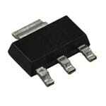
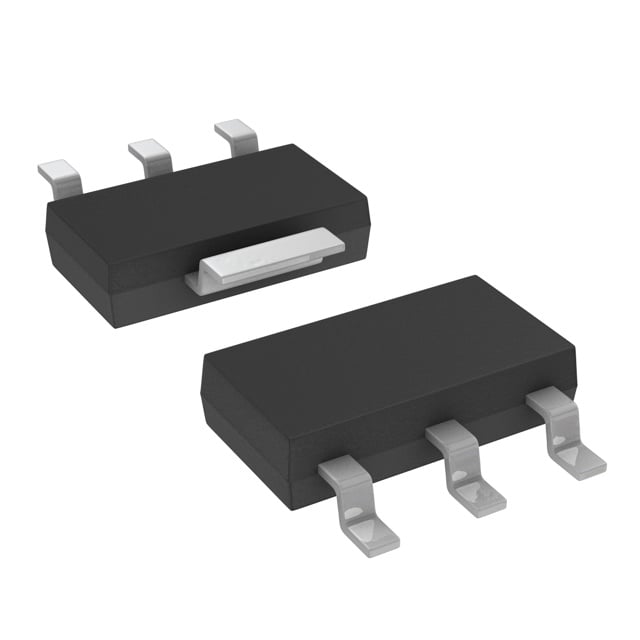
| 描述 | IC REG LDO ADJ 1A SOT223低压差稳压器 1.25-18V ADJ 1.0A |
| 产品分类 | |
| 品牌 | ON Semiconductor |
| 产品手册 | |
| 产品图片 |
|
| rohs | 符合RoHS无铅 / 符合限制有害物质指令(RoHS)规范要求 |
| 产品系列 | 电源管理 IC,低压差稳压器,ON Semiconductor NCV1117STAT3G- |
| 数据手册 | |
| 产品型号 | NCV1117STAT3G |
| 产品种类 | 低压差稳压器 |
| 供应商器件封装 | SOT-223 |
| 其它名称 | NCV1117STAT3GOSDKR |
| 包装 | Digi-Reel® |
| 参考电压 | 1.262 V |
| 商标 | ON Semiconductor |
| 回动电压—最大值 | 1.1 V at 100 mA |
| 安装类型 | 表面贴装 |
| 安装风格 | SMD/SMT |
| 封装 | Reel |
| 封装/外壳 | TO-261-4,TO-261AA |
| 封装/箱体 | SOT-223-4 |
| 工作温度 | -40°C ~ 125°C |
| 工厂包装数量 | 4000 |
| 最大工作温度 | + 125 C |
| 最大输入电压 | 20 V |
| 最小工作温度 | - 40 C |
| 标准包装 | 1 |
| 电压-跌落(典型值) | 1.07V @ 800mA |
| 电压-输入 | 最高 20V |
| 电压-输出 | 1.25 V ~ 18.8 V |
| 电压调节准确度 | 1 % |
| 电流-输出 | 1A |
| 电流-限制(最小值) | 1A |
| 稳压器拓扑 | 正,可调式 |
| 稳压器数 | 1 |
| 系列 | NCV1117 |
| 线路调整率 | 0.04 % |
| 负载调节 | 0.2 % |
| 输出电压 | 1.25 V to 18.8 V |
| 输出电流 | 1 A |
| 输出端数量 | 1 Output |
| 输出类型 | Adjustable |


PDF Datasheet 数据手册内容提取
NCP1117, NCV1117 1.0 A Low-Dropout Positive Fixed and Adjustable Voltage Regulators The NCP1117 series are low dropout positive voltage regulators that are capable of providing an output current that is in excess of 1.0 A www.onsemi.com with a maximum dropout voltage of 1.2 V at 800 mA over temperature. This series contains nine fixed output voltages of 1.5 V, 1.8 V, 1.9 V, 2.0 V, 2.5 V, 2.85 V, 3.3 V, 5.0 V, and 12 V that have no minimum load requirement to maintain regulation. Also included is an adjustable output version that can be programmed from 1.25 V to SOT−223 DPAK 18.8 V with two external resistors. On chip trimming adjusts the ST SUFFIX DT SUFFIX reference/output voltage to within ±1.0% accuracy. Internal protection CASE 318H CASE 369C features consist of output current limiting, safe operating area PIN CONFIGURATION compensation, and thermal shutdown. The NCP1117 series can operate with up to 20 V input. Devices are available in SOT−223 and Tab DPAK packages. Features • 123 Output Current in Excess of 1.0 A • SOT−223 1.2 V Maximum Dropout Voltage at 800 mA Over Temperature (Top View) • Fixed Output Voltages of 1.5 V, 1.8 V, 1.9 V, 2.0 V, 2.5 V, 2.85 V, 3.3 V, 5.0 V, and 12 V Tab • Adjustable Output Voltage Option • No Minimum Load Requirement for Fixed Voltage Output Devices • Reference/Output Voltage Trimmed to ±1.0% 2 1 3 • Current Limit, Safe Operating and Thermal Shutdown Protection DPAK • Operation to 20 V Input (Top View) • NCV Prefix for Automotive and Other Applications Requiring Unique Site and Control Change Requirements; AEC−Q100 Pin: 1. Adjust/Ground 2. Output Qualified and PPAP Capable 3. Input • These are Pb-Free Devices Heatsink tab is connected to Pin 2. Applications • Consumer and Industrial Equipment Point of Regulation ORDERING INFORMATION • See detailed ordering and shipping information in the package Active SCSI Termination for 2.85 V Version dimensions section on page 12 of this data sheet. • Switching Power Supply Post Regulation • Hard Drive Controllers DEVICE MARKING INFORMATION • Battery Chargers See general marking information in the device marking section on page 14 of this data sheet. © Semiconductor Components Industries, LLC, 2017 1 Publication Order Number: July, 2018 − Rev. 29 NCP1117/D
NCP1117, NCV1117 TYPICAL APPLICATIONS 110 (cid:3) Input 3 NCP1117 2 Output Input 3 NCP1117 2 Output 3 NCP1117 2 110 (cid:3) XT285 18 to 27 XTXX XTA 10 + +22 110 (cid:3) 10 + +10 10 + +10 (cid:2)F 1 (cid:2)F Lines (cid:2)F 1 (cid:2)F (cid:2)F 1 (cid:2)F 4.75 V + to 110 (cid:3) 5.25 V Figure 1. Fixed Figure 2. Adjustable Figure 3. Active SCSI Bus Terminator Output Regulator Output Regulator MAXIMUM RATINGS Rating Symbol Value Unit Input Voltage (Note 1) Vin 20 V Output Short Circuit Duration (Notes 2 and 3) − Infinite − Power Dissipation and Thermal Characteristics Case 318H (SOT−223) Power Dissipation (Note 2) PD Internally Limited W Thermal Resistance, Junction−to−Ambient, Minimum Size Pad R(cid:4)JA 160 °C/W Thermal Resistance, Junction−to−Case R(cid:4)JC 15 °C/W Case 369A (DPAK) Power Dissipation (Note 2) PD Internally Limited W Thermal Resistance, Junction−to−Ambient, Minimum Size Pad R(cid:4)JA 67 °C/W Thermal Resistance, Junction−to−Case R(cid:4)JC 6.0 °C/W Maximum Die Junction Temperature Range T −55 to 150 °C J Storage Temperature Range T −65 to 150 °C stg Operating Ambient Temperature Range TA °C NCP1117 0 to +125 NCV1117 −40 to +125 Stresses exceeding those listed in the Maximum Ratings table may damage the device. If any of these limits are exceeded, device functionality should not be assumed, damage may occur and reliability may be affected. 1. This device series contains ESD protection and exceeds the following tests: Human Body Model (HBM), Class 2, 2000 V Machine Model (MM), Class B, 200 V Charge Device Model (CDM), Class IV, 2000 V. 2. Internal thermal shutdown protection limits the die temperature to approximately 175°C. Proper heatsinking is required to prevent activation. The maximum package power dissipation is: TJ(max)(cid:3)TA PD(cid:2) R(cid:4)JA 3. The regulator output current must not exceed 1.0 A with Vin greater than 12 V. www.onsemi.com 2
NCP1117, NCV1117 ELECTRICAL CHARACTERISTICS (Cin = 10 (cid:2)F, Cout = 10 (cid:2)F, for typical value TA = 25°C, for min and max values TA is the operating ambient temperature range that applies unless otherwise noted.) (Note 4) Characteristic Symbol Min Typ Max Unit Reference Voltage, Adjustable Output Devices V V ref (Vin–Vout = 2.0 V, Iout = 10 mA, TA = 25°C) 1.238 1.25 1.262 (Vin–Vout = 1.4 V to 10 V, Iout = 10 mA to 800 mA) (Note 4) 1.225 − 1.270 Output Voltage, Fixed Output Devices V V out 1.5 V (Vin = 3.5 V, Iout = 10 mA, TA = 25 °C) 1.485 1.500 1.515 (Vin = 2.9 V to 11.5 V, Iout = 0 mA to 800 mA) (Note 4) 1.470 − 1.530 1.8 V (Vin = 3.8 V, Iout = 10 mA, TA = 25 °C) 1.782 1.800 1.818 (Vin = 3.2 V to 11.8 V, Iout = 0 mA to 800 mA) (Note 4) 1.755 − 1.845 1.9 V (Vin = 3.9 V, Iout = 10 mA, TA = 25 °C) 1.872 1.900 1.929 (Vin = 3.3 V to 11.9 V, Iout = 0 mA to 800 mA) (Note 4) 1.862 1.900 1.938 2.0 V (Vin = 4.0 V, Iout = 10 mA, TA = 25 °C) 1.970 2.000 2.030 (Vin = 3.4 V to 12 V, Iout = 0 mA to 800 mA) (Note 4) 1.960 − 2.040 2.5 V (Vin = 4.5 V, Iout = 10 mA, TA = 25 °C) 2.475 2.500 2.525 (Vin = 3.9 V to 10 V, Iout = 0 mA to 800 mA,) (Note 4) 2.450 − 2.550 2.85 V (Vin = 4.85 V, Iout = 10 mA, TA = 25 °C) 2.821 2.850 2.879 (Vin = 4.25 V to 10 V, Iout = 0 mA to 800 mA) (Note 4) 2.790 − 2.910 (Vin = 4.0 V, Iout = 0 mA to 500 mA) (Note 4) 2.790 − 2.910 3.3 V (Vin = 5.3 V, Iout = 10 mA, TA = 25 °C) 3.267 3.300 3.333 (Vin = 4.75 V to 10 V, Iout = 0 mA to 800 mA) (Note 4) 3.235 − 3.365 5.0 V (Vin = 7.0 V, Iout = 10 mA, TA = 25 °C) 4.950 5.000 5.050 (Vin = 6.5 V to 12 V, Iout = 0 mA to 800 mA) (Note 4) 4.900 − 5.100 12 V (Vin = 14 V, Iout = 10 mA, TA = 25 °C) 11.880 12.000 12.120 (Vin = 13.5 V to 20 V, Iout = 0 mA to 800 mA) (Note 4) 11.760 − 12.240 Line Regulation (Note 5) Adjustable (Vin = 2.75 V to 16.25 V, Iout = 10 mA) Regline − 0.04 0.1 % 1.5 V (Vin = 2.9 V to 11.5 V, Iout = 0 mA) − 0.3 1.0 mV 1.8 V (Vin = 3.2 V to 11.8 V, Iout = 0 mA) − 0.4 1.0 1.9 V (Vin = 3.3 V to 11.9 V, Iout = 0 mA) − 0.5 2.5 2.0 V (Vin = 3.4 V to 12 V, Iout = 0 mA) − 0.5 2.5 2.5 V (Vin = 3.9 V to 10 V, Iout = 0 mA) − 0.5 2.5 2.85 V (Vin = 4.25 V to 10 V, Iout = 0 mA) − 0.8 3.0 3.3 V (Vin = 4.75 V to 15 V, Iout = 0 mA) − 0.8 4.5 5.0 V (Vin = 6.5 V to 15 V, Iout = 0 mA) − 0.9 6.0 12 V (Vin = 13.5 V to 20 V, Iout = 0 mA) − 1.0 7.5 Load Regulation (Note 5) Adjustable (Iout = 10 mA to 800 mA, Vin = 4.25 V) Regline − 0.2 0.4 % 1.5 V (Iout = 0 mA to 800 mA, Vin = 2.9 V) − 2.3 5.5 mV 1.8 V (Iout = 0 mA to 800 mA, Vin = 3.2 V) − 2.6 6.0 1.9 V (Iout = 0 mA to 800 mA, Vin = 3.3 V) − 2.7 6.0 2.0 V (Iout = 0 mA to 800 mA, Vin = 3.4 V) − 3.0 6.0 2.5 V (Iout = 0 mA to 800 mA, Vin = 3.9 V) − 3.3 7.5 2.85 V (Iout = 0 mA to 800 mA, Vin = 4.25 V) − 3.8 8.0 3.3 V (Iout = 0 mA to 800 mA, Vin = 4.75 V) − 4.3 10 5.0 V (Iout = 0 mA to 800 mA, Vin = 6.5 V) − 6.7 15 12 V (Iout = 0 mA to 800 mA, Vin = 13.5 V) − 16 28 Dropout Voltage (Measured at Vout − 100 mV) Vin−Vout V (I = 100 mA) − 0.95 1.10 out (I = 500 mA) − 1.01 1.15 out (I = 800 mA) − 1.07 1.20 out Output Current Limit (Vin−Vout = 5.0 V, TA = 25°C, Note 6) Iout 1000 1500 2200 mA Minimum Required Load Current for Regulation, Adjustable Output Devices IL(min) − 0.8 5.0 mA (Vin = 15 V) www.onsemi.com 3
NCP1117, NCV1117 ELECTRICAL CHARACTERISTICS (continued) (Cin = 10 (cid:2)F, Cout = 10 (cid:2)F, for typical value TA = 25°C, for min and max values TA is the operating ambient temperature range that applies unless otherwise noted.) (Note 4) Characteristic Symbol Min Typ Max Unit Quiescent Current I mA Q 1.5 V (Vin = 11.5 V) − 3.6 10 1.8 V (Vin = 11.8 V) − 4.2 10 1.9 V (Vin = 11.9 V) − 4.3 10 2.0 V (Vin = 12 V) − 4.5 10 2.5 V (Vin = 10 V) − 5.2 10 2.85 V (Vin = 10 V) − 5.5 10 3.3 V (Vin = 15 V) − 6.0 10 5.0 V (Vin = 15 V) − 6.0 10 12 V (Vin = 20 V) − 6.0 10 Thermal Regulation (TA = 25°C, 30 ms Pulse) − 0.01 0.1 %/W Ripple Rejection (Vin−Vout = 6.4 V, Iout = 500 mA, 10 Vpp 120 Hz Sinewave) RR dB Adjustable 67 73 − 1.5 V 66 72 − 1.8 V 66 70 − 1.9 V 66 72 − 2.0 V 64 70 − 2.5 V 62 68 − 2.85 V 62 68 − 3.3 V 60 64 − 5.0 V 57 61 − 12 V 50 54 − Adjustment Pin Current (Vin = 11.25 V, Iout = 800 mA) Iadj − 52 120 (cid:2)A Adjust Pin Current Change (cid:5)I − 0.4 5.0 (cid:2)A adj (Vin−Vout = 1.4 V to 10 V, Iout = 10 mA to 800 mA) Temperature Stability S − 0.5 − % T Long Term Stability (TA = 25°C, 1000 Hrs End Point Measurement) St − 0.3 − % RMS Output Noise (f = 10 Hz to 10 kHz) N − 0.003 − %V out Product parametric performance is indicated in the Electrical Characteristics for the listed test conditions, unless otherwise noted. Product performance may not be indicated by the Electrical Characteristics if operated under different conditions. 4. NCP1117: Tlow = 0°C , Thigh = 125°C NCV1117: Tlow = −40°C, Thigh = 125°C 5. Low duty cycle pulse techniques are used during testing to maintain the junction temperature as close to ambient as possible. 6. The regulator output current must not exceed 1.0 A with Vin greater than 12 V. www.onsemi.com 4
NCP1117, NCV1117 2.0 1.4 HANGE (%) 11..05 IVoiunt == V1o0u mt +A 3.0 V A12..d85j ,VV 1, .25. 0V ,V, LTAGE (V) 11..02 TJ = −40°C TJ = 25°C C O E 0.5 V G T 0.8 TA 0 OU TJ = 125°C OL OP 0.6 T V−0.5 DR TPU−1.0 25..805 V V, 1, 32..30 VV, , out 0.4 U V , Out−1.5 V − in 0.2 Load pulsed at 1.0% duty cycle o V−2.0 0 −50 −25 0 25 50 75 100 125 150 0 200 400 600 800 1000 TA, AMBIENT TEMPERATURE (°C) Iout, OUTPUT CURRENT (mA) Figure 4. Output Voltage Change Figure 5. Dropout Voltage vs. Temperature vs. Output Current 2.0 2.0 TJ = 25°C A) A) 1.8 T ( 1.5 T ( N N E E R R R R 1.6 U U C 1.0 C T T PU PU 1.4 T T U U O 0.5 O , ut , ut 1.2 Io Io Vin = 5.0 V Load pulsed at 1.0% duty cycle Load pulsed at 1.0% duty cycle 0 1.0 0 2 4 6 8 10 12 14 16 18 20 −50 −25 0 25 50 75 100 125 150 Vin − Vout, VOLTAGE DIFFERENTIAL (V) TA, AMBIENT TEMPERATURE (°C) Figure 6. Output Short Circuit Current Figure 7. Output Short Circuit Current vs. Differential Voltage vs. Temperature 100 %) 10 A) E ( (cid:2) G T ( 80 AN 5.0 N H E C RR T 0 U 60 N C E N RR−5.0 PI U ST 40 T C U N−10 J E D C , Aadj 20 Iout = 10 mA UIES−15 I Q 0 Q,−20 −50 −25 0 25 50 75 100 125 150 I −50 −25 0 25 50 75 100 125 150 TA, AMBIENT TEMPERATURE (°C) TA, AMBIENT TEMPERATURE (°C) Figure 8. Adjust Pin Current Figure 9. Quiescent Current Change vs. Temperature vs. Temperature www.onsemi.com 5
NCP1117, NCV1117 100 100 fripple = 120 Hz Vripple (cid:4) 3.0 VP−P Vripple (cid:4) 0.5 VP−P dB) 80 Vripple (cid:4) 3.0 VP−P dB) 80 Vin − Vout (cid:5) 3.0 V N ( N ( O O TI TI RR, RIPPLE REJEC 246000 VVCCTAoioanu ud =t−tj === 2V 5521o°.u500Ct (cid:2)(cid:2)=VFF 3 .0 V fVrirpippplele = (cid:4) 2 00 .k5H VzP−P RR, RIPPLE REJEC 246000 CTVVICCoAaoioaun du=udt jt− tj= =2=== V 05 2521o.°05.u5C000t A (cid:2)(cid:2) =V(cid:2)FF F3, ,.f 0 f> (cid:4)V 6 06 0H zHz Vin − Vout (cid:5) Vdropout 0 0 0 200 400 600 800 1000 10 100 1.0 k 10 k 100 k Iout, OUTPUT CURRENT (mA) fripple, RIPPLE FREQUENCY (Hz) Figure 10. NCP1117XTA Ripple Rejection Figure 11. NCP1117XTA Ripple Rejection vs. Output Current vs. Frequency 100 (cid:3)) 10 Region of Stability Vin = 3.0 V CE ( Vin = 3.0 V F) Vout = 1.25 V AN Vout = 1.25 V (cid:2)ANCE ( 10 TICloJina = d= =2 1 550° Cm(cid:2)FA M− L1C AC RESIST 1 Region of Stability CCTJion u= t= =2 15 10°0 C(cid:2) (cid:2)FF MLCC T S CI E A RI P E A Region of Instability S T C 1 NT 0.1 U E P L T A U V O UI Q E Region of Instability 00.1.001 0.01 0.1 1 10 R, 0.010 100 200 300 400 500 600 700 800 900 1000 S E ESR, EQUIVALENT SERIES RESISTANCE ((cid:3)) Iout, OUTPUT CURRENT (mA) Figure 12. Output Capacitance vs. ESR Figure 13. Typical ESR vs. Output Current 350E−9 1 A Cin = 10 (cid:2)F Tantalum 300E−9 Cout = 10 (cid:2)F Tantalum 0.5 A Vin − Vout = 3.0 V 250E−9 z) 200E−9 H sqrt ( 150E−9 0.1 A V/ 100E−9 50E−9 0 10 100 1.0 k 10 k 100 k FREQUENCY (Hz) Figure 14. Output Spectral Noise Density vs. Frequency, V = 1V5 out www.onsemi.com 6
NCP1117, NCV1117 E INPUTVOLTAGE (V)54..2255 CCIToAioun ut = t== = 2 10 51..0°10C (cid:2)A(cid:2)FF OUTPUT VOLTAGDEVIATION (V)−00..110 CCionu t= = 1 100 (cid:2) (cid:2)FF PUT VOLTAGEVIATION (mV)−22000 D CURRENTHANGE (A) 0.50 PTVAirne =l=o 2a45d.5° =C V 0.1 A TE AC UD O O L 0 40 80 120 160 200 0 40 80 120 160 200 t, TIME ((cid:2)s) t, TIME ((cid:2)s) Figure 15. NCP1117XT285 Figure 16. NCP1117XT285 Line Transient Response Load Transient Response E TE (V) CCionu t= = 1 1.00 (cid:2)(cid:2)FF OLTAGON (V) 0.1 INPUVOLTAG 76..55 IToAu t= = 2 05.°1C A OUTPUT VDEVIATI−0.10 CCionu t= = 1 100 (cid:2) (cid:2)FF E Vin = 6.5 V OLTAGN (mV) 20 RRENTE (A) PTAre =lo 2a5d° =C 0.1 A T VTIO 0 CUNG 0.5 OUTPUDEVIA−20 LOAD CHA 0 0 40 80 120 160 200 0 40 80 120 160 200 t, TIME ((cid:2)s) t, TIME ((cid:2)s) Figure 17. NCP1117XT50 Figure 18. NCP1117XT50 Line Transient Response Load Transient Response E TE (V) CCionu t= = 1 1.00 (cid:2)(cid:2)FF OLTAGON (V) 0.1 INPUVOLTAG1143..55 IToAu t= = 2 05.°1C A UTPUT VDEVIATI−0.10 Cin = 10 (cid:2)F O Cout = 10 (cid:2)F OLTAGEN (mV) 20 RRENTE (A) VPTAirne =l=o 2a15d3° .=C5 0V.1 A VO 0 UG 0.5 T TI CN TPUEVIA−20 OAD CHA 0 OUD L 0 40 80 120 160 200 0 40 80 120 160 200 t, TIME ((cid:2)s) t, TIME ((cid:2)s) Figure 19. NCP1117XT12 Line Figure 20. NCP1117XT12 Load Transient Response Transient Response www.onsemi.com 7
NCP1117, NCV1117 W) 180 1.6 N ( E, O ANCCW) 160 PD(max) for TA = 50°C 1.4 PATI ESIST°AIR ( 140 2.0 oz. Copper 1.2 DISSI MAL RN−TO− 120 MSiizneim Puamd ÎÎÎÎL ÎÎ 1.0 OWER , THERJAJUNCTIO 18000 LÎÎÎ 00..68 XIMUM P R(cid:4) R(cid:4)JA MA 600 5.0 10 15 20 25 300.4 , PD L, LENGTH OF COPPER (mm) Figure 21. SOT−223 Thermal Resistance and Maximum Power Dissipation vs. P.C.B. Copper Length W) E, 100 PD(max) for TA = 50°C 1.6 ON ( NCW) 90 1.4 ATI AC P AL RESIST°−TO−AIR ( 7800 MSiizneim Puamd 2ÎÎÎ.L0 ozÎÎÎ. CLoÎÎÎpperÎÎÎ11..02 WER DISSI MN O , THERJAJUNCTIO 5600 ÎÎÎÎ00..68 XIMUM P R(cid:4) R(cid:4)JA A M 40 0.4 , D 0 5.0 10 15 20 25 30 P L, LENGTH OF COPPER (mm) Figure 22. DPAK Thermal Resistance and Maximum Power Dissipation vs. P.C.B. Copper Length www.onsemi.com 8
NCP1117, NCV1117 APPLICATIONS INFORMATION Introduction Frequency compensation for the regulator is provided by The NCP1117 features a significant reduction in dropout capacitor C and its use is mandatory to ensure output out voltage along with enhanced output voltage accuracy and stability. A minimum capacitance value of 4.7 (cid:2)F with an temperature stability when compared to older industry equivalent series resistance (ESR) that is within the limits of standard three−terminal adjustable regulators. These 33 m(cid:3) (typ) to 2.2 (cid:3) is required. See Figures 12 and 13. The devices contain output current limiting, safe operating area capacitor type can be ceramic, tantalum, or aluminum compensation and thermal shutdown protection making electrolytic as long as it meets the minimum capacitance them designer friendly for powering numerous consumer value and ESR limits over the circuit’s entire operating and industrial products. The NCP1117 series is pin temperature range. Higher values of output capacitance can compatible with the older LM317 and its derivative device be used to enhance loop stability and transient response with types. the additional benefit of reducing output noise. Output Voltage Input Output The typical application circuits for the fixed and 3 NCP1117 2 XTA aTdhjeu satdajbulset aobultep duet vreicgeusl aatroer sf laoraet isnhgo vwonl tiang Fe irgeugruelsa 2to3r sa.n Td h2e4y. Cin + 1 Vref R1 +Cout develop and maintain the nominal 1.25 V reference voltage Iadj + between the output and adjust pins. The reference voltage is R2 Cadj programmed to a constant current source by resistor R1, and this current flows through R2 to ground to set the output (cid:6) (cid:8) voltage. The programmed current level is usually selected to Vout(cid:2)Vref 1(cid:7)R2 (cid:7)IadjR2 be greater than the specified 5.0 mA minimum that is R1 required for regulation. Since the adjust pin current, Iadj, is Figure 24. Adjustable Output Regulator significantly lower and constant with respect to the programmed load current, it generates a small output The output ripple will increase linearly for fixed and voltage error that can usually be ignored. For the fixed adjustable devices as the ratio of output voltage to the output devices R1 and R2 are included within the device and reference voltage increases. For example, with a 12 V the ground current Ignd, ranges from 3.0 mA to 5.0 mA regulator, the output ripple will increase by 12 V/1.25 V or depending upon the output voltage. 9.6 and the ripple rejection will decrease by 20 log of this ratio or 19.6 dB. The loss of ripple rejection can be restored External Capacitors to the values shown with the addition of bypass capacitor Input bypass capacitor C may be required for regulator in Cadj, shown in Figure 24. The reactance of Cadj at the ripple stability if the device is located more than a few inches from frequency must be less than the resistance of R1. The value the power source. This capacitor will reduce the circuit’s of R1 can be selected to provide the minimum required load sensitivity when powered from a complex source impedance current to maintain regulation and is usually in the range of and significantly enhance the output transient response. The 100 (cid:3) to 200 (cid:3). input bypass capacitor should be mounted with the shortest panodss igbrleo utnradc kt elremngintha lsd.i reAc tl1y0 a c(cid:2)rFo ssc ethraem reicg uolart otra’sn tianlpuumt Cadj(cid:9)2(cid:6)frip1pleR1 capacitor should be adequate for most applications. The minimum required capacitance can be calculated from the above formula. When using the device in an application that is powered from the AC line via a transformer and a full wave bridge, the value for Cadj is: Input 3 NCP1117 2 Output fripple(cid:2)120Hz, R1(cid:2)120(cid:3), thenCadj(cid:9)11.1(cid:2)F XTXX + + The value for Cadj is significantly reduced in applications Cin 1 Cout where the input ripple frequency is high. If used as a post Ignd regulator in a switching converter under the following conditions: fripple(cid:2)50kHz, R1(cid:2)120(cid:3), thenCadj(cid:9)0.027(cid:2)F Figure 23. Fixed Output Regulator Figures 10 and 11 shows the level of ripple rejection that is obtainable with the adjust pin properly bypassed. www.onsemi.com 9
NCP1117, NCV1117 Protection Diodes The second condition is that the ground end of R2 should be The NCP1117 family has two internal low impedance connected directly to the load. This allows true Kelvin diode paths that normally do not require protection when sensing where the regulator compensates for the voltage used in the typical regulator applications. The first path drop caused by wiring resistance RW −. connects between V and V , and it can withstand a peak out in surge current of about 15 A. Normal cycling of Vin cannot Input 3 NCP1117 2 RW+ Output generate a current surge of this magnitude. Only when V in XTA i5s0 s (cid:2)hFo,r teitd boerc cormowesb aproresdsi btole g rfoour ndde avnicde C doaumt iasg ger etaot eor ctchuarn. Cin + 1 R1R2 + Cout RLoeamdote Under these conditions, diode D1 is required to protect the device. The second path connects between Cadj and Vout, and it can withstand a peak surge current of about 150 mA. Protection diode D2 is required if the output is shorted or crowbarred to ground and Cadj is greater than 1.0 (cid:2)F. RW− Figure 26. Load Sensing D1 1N4001 Thermal Considerations This series contains an internal thermal limiting circuit Input Output 3 NCP1117 2 that is designed to protect the regulator in the event that the XTA Cin + 1 R1 D1N24001 +Cout macatixviamteudm, typjuicnacltliyo na t 1t7em5°pCe,r athtuer ree guisl atoerx coeuetpduedt .s wWitchheens off and then back on as the die cools. As a result, if the device + R2 Cadj is continuously operated in an overheated condition, the output will appear to be oscillating. This feature provides protection from a catastrophic device failure due to accidental overheating. It is not intended to be used as a Figure 25. Protection Diode Placement substitute for proper heatsinking. The maximum device power dissipation can be calculated by: A combination of protection diodes D1 and D2 may be TJ(max)(cid:3)TA irse qgureiraetder i nth tahne 5 e0v e(cid:2)nFt. tThhaet Vpeina kis c suhrorertnetd c taop agbroiluitnyd s atantde dC faodrj PD(cid:2) R(cid:4)JA The devices are available in surface mount SOT−223 and the internal diodes are for a time of 100 (cid:2)s with a junction DPAK packages. Each package has an exposed metal tab temperature of 25°C. These values may vary and are to be that is specifically designed to reduce the junction to air used as a general guide. thermal resistance, R(cid:4)JA, by utilizing the printed circuit Load Regulation board copper as a heat dissipater. Figures 21 and 22 show The NCP1117 series is capable of providing excellent typical R(cid:4)JA values that can be obtained from a square load regulation; but since these are three terminal devices, pattern using economical single sided 2.0 ounce copper only partial remote load sensing is possible. There are two board material. The final product thermal limits should be conditions that must be met to achieve the maximum tested and quantified in order to insure acceptable available load regulation performance. The first is that the performance and reliability. The actual R(cid:4)JA can vary top side of programming resistor R1 should be connected as considerably from the graphs shown. This will be due to any close to the regulator case as practicable. This will minimize changes made in the copper aspect ratio of the final layout, the voltage drop caused by wiring resistance RW + from adjacent heat sources, and air flow. appearing in series with reference voltage that is across R1. www.onsemi.com 10
NCP1117, NCV1117 Constant Current Input Output 3 NCP1117 2 Output Input R XTA 3 NCP1117 2 10 + +10 R1 XTA (cid:2)F 1 (cid:2)F 10 + + 10 50 k 1N4001 (cid:2)F 1 (cid:2)F R2 2N2907 10 Iout(cid:2)Vref(cid:7)Iadj (cid:2)F R Figure 27. Constant Current Regulator Figure 28. Slow Turn−On Regulator Input Output 3 NCP1117 2 XTA 10 + +10 (cid:2)F 1 R1 (cid:2)F Input Output 3 NCP1117 2 XTA 10 + +10 R2 (cid:2)F 1 120 (cid:2)F 2N2222 Output Control 1.0 k 360 2N2222 On Off 1.0 k Output Voltage Control Resistor R2 sets the maximum output voltage. Each Vout(Off)(cid:2)Vref transistor reduces the output voltage when turned on. Figure 29. Regulator with Shutdown Figure 30. Digitally Controlled Regulator Input Output 3 NCP1117 2 XT50 10 + +10 (cid:2)F 1 (cid:2)F 50 (cid:3) Input Output 3 NCP1117 2 RCHG 5.3 V AC Line XT50 5.0 V to 5.0 V Battery 10 + +10 12 V 3 NCP1117 2 (cid:2)F 1 (cid:2)F XT50 + 10 + +10 6.6 V (cid:2)F 1 2.0 k (cid:2)F − The 50 (cid:3) resistor that is in series with the ground pin of the upper regulator level shifts its output 300 mV higher than the lower regulator. This keeps the lower regulator off until the input source is removed. Figure 31. Battery Backed−Up Power Supply Figure 32. Adjusting Output of Fixed Voltage Regulators www.onsemi.com 11
NCP1117, NCV1117 ORDERING INFORMATION Device Nominal Output Voltage Package Shipping† NCP1117STAT3G Adjustable SOT−223 4000 / Tape & Reel (Pb−Free) NCV1117STAT3G* Adjustable SOT−223 4000 / Tape & Reel (Pb−Free) NCP1117ST15T3G 1.5 SOT−223 4000 / Tape & Reel (Pb−Free) NCV1117ST15T3G* 1.5 SOT−223 4000 / Tape & Reel (Pb−Free) NCP1117ST18T3G 1.8 SOT−223 4000 / Tape & Reel (Pb−Free) NCV1117ST18T3G* 1.8 SOT−223 4000 / Tape & Reel (Pb−Free) NCP1117ST20T3G 2.0 SOT−223 4000 / Tape & Reel (Pb−Free) NCV1117ST20T3G* 2.0 SOT−223 4000 / Tape & Reel (Pb−Free) NCP1117ST25T3G 2.5 SOT−223 4000 / Tape & Reel (Pb−Free) NCV1117ST25T3G* 2.5 SOT−223 4000 / Tape & Reel (Pb−Free) NCP1117ST285T3G 2.85 SOT−223 4000 / Tape & Reel (Pb−Free) NCP1117ST33T3G 3.3 SOT−223 4000 / Tape & Reel (Pb−Free) NCV1117ST33T3G* 3.3 SOT−223 4000 / Tape & Reel (Pb−Free) NCP1117ST50T3G 5.0 SOT−223 4000 / Tape & Reel (Pb−Free) NCV1117ST50T3G* 5.0 SOT−223 4000 / Tape & Reel (Pb−Free) NCP1117ST12T3G 12 SOT−223 4000 / Tape & Reel (Pb−Free) NCV1117ST12T3G* 12 SOT−223 4000 / Tape & Reel (Pb−Free) NCP1117DTAG Adjustable DPAK 75 Units / Rail (Pb−Free) NCP1117DTARKG Adjustable DPAK 2500 / Tape & Reel (Pb−Free) NCV1117DTARKG* Adjustable DPAK 2500 / Tape & Reel (Pb−Free) NCP1117DTAT5G Adjustable DPAK 2500 / Tape & Reel (Pb−Free) NCP1117DT15G 1.5 DPAK 75 Units / Rail (Pb−Free) NCP1117DT15RKG 1.5 DPAK 2500 / Tape & Reel (Pb−Free) NCV1117DT15RKG* 1.5 DPAK 2500 / Tape & Reel (Pb−Free) NCP1117DT18G 1.8 DPAK 75 Units / Rail (Pb−Free) †For information on tape and reel specifications, including part orientation and tape sizes, please refer to our Tape and Reel Packaging Specifications Brochure, BRD8011/D. *NCV Prefix for Automotive and Other Applications Requiring Unique Site and Control Change Requirements; AEC−Q100 Qualified and PPAP Capable www.onsemi.com 12
NCP1117, NCV1117 ORDERING INFORMATION (continued) Device Nominal Output Voltage Package Shipping† NCP1117DT18RKG 1.8 DPAK 2500 / Tape & Reel (Pb−Free) NCV1117DT18RKG* 1.8 DPAK 2500 / Tape & Reel (Pb−Free) NCP1117DT18T5G 1.8 DPAK 2500 / Tape & Reel (Pb−Free) NCV1117DT18T5G* 1.8 DPAK 2500 / Tape & Reel (Pb−Free) NCP1117DT19RKG 1.9 DPAK 2500 / Tape & Reel (Pb−Free) NCP1117DT20G 2.0 DPAK 75 Units / Rail (Pb−Free) NCP1117DT20RKG 2.0 DPAK 2500 / Tape & Reel (Pb−Free) NCV1117DT20RKG* 2.0 DPAK 2500 / Tape & Reel (Pb−Free) NCP1117DT25G 2.5 DPAK 75 Units / Rail (Pb−Free) NCP1117DT25RKG 2.5 DPAK 2500 / Tape & Reel (Pb−Free) NCV1117DT25RKG* 2.5 DPAK 2500 / Tape & Reel (Pb−Free) NCP1117DT25T5G 2.5 DPAK 2500 / Tape & Reel (Pb−Free) NCP1117DT285G 2.85 DPAK 75 Units / Rail (Pb−Free) NCP1117DT285RKG 2.85 DPAK 2500 / Tape & Reel (Pb−Free) NCP1117DT33G 3.3 DPAK 75 Units / Rail (Pb−Free) NCP1117DT33RKG 3.3 DPAK 2500 / Tape & Reel (Pb−Free) NCV1117DT33T4G* 3.3 DPAK 2500 / Tape & Reel (Pb−Free) NCP1117DT33T5G 3.3 DPAK 2500 / Tape & Reel (Pb−Free) NCV1117DT33T5G* 3.3 DPAK 2500 / Tape & Reel (Pb−Free) NCP1117DT50G 5.0 DPAK 75 Units / Rail (Pb−Free) NCP1117DT50RKG 5.0 DPAK 2500 / Tape & Reel (Pb−Free) NCV1117DT50RKG* 5.0 DPAK 2500 / Tape & Reel (Pb−Free) NCP1117DT12G 12 DPAK 75 Units / Rail (Pb−Free) NCP1117DT12RKG 12 DPAK 2500 / Tape & Reel (Pb−Free) NCV1117DT12RKG* 12 DPAK 2500 / Tape & Reel (Pb−Free) †For information on tape and reel specifications, including part orientation and tape sizes, please refer to our Tape and Reel Packaging Specifications Brochure, BRD8011/D. *NCV Prefix for Automotive and Other Applications Requiring Unique Site and Control Change Requirements; AEC−Q100 Qualified and PPAP Capable www.onsemi.com 13
NCP1117, NCV1117 MARKING DIAGRAMS − NCP PREFIX SOT−223 ST SUFFIX CASE 318H AYW AYW AYW AYW AYW AYW 117−A(cid:2) 17−15(cid:2) 17−18(cid:2) 17−19(cid:2) 117−2(cid:2) 17−25(cid:2) (cid:2) (cid:2) (cid:2) (cid:2) (cid:2) (cid:2) 1 2 3 1 2 3 1 2 3 1 2 3 1 2 3 1 2 3 Adjustable 1.5 V 1.8 V 1.9 V 2.0 V 2.5 V AYW AYW AYW AYW 7−285(cid:2) 17−33(cid:2) 117−5(cid:2) 17−12(cid:2) (cid:2) (cid:2) (cid:2) (cid:2) 1 2 3 1 2 3 1 2 3 1 2 3 2.85 V 3.3 V 5.0 V 12 V DPAK DT SUFFIX CASE 369C 117AJG 17−15G 17−18G 17−19G 117−2G 17−25G ALYWW ALYWW ALYWW ALYWW ALYWW ALYWW 2 2 2 2 2 2 1 3 1 3 1 3 1 3 1 3 1 3 Adjustable 1.5 V 1.8 V 1.9 V 2.0 V 2.5 V 17285G 17−33G 117−5G 17−12G ALYWW ALYWW ALYWW ALYWW 2 2 2 2 1 3 1 3 1 3 1 3 2.85 V 3.3 V 5.0 V 12 V A = Assembly Location L = Wafer Lot Y = Year WW, W = Work Week (cid:2) or G = Pb−Free Package (Note: Microdot may be in either location) www.onsemi.com 14
NCP1117, NCV1117 MARKING DIAGRAMS − NCV PREFIX SOT−223 ST SUFFIX CASE 318H AYW AYW AYW AYW 117AV(cid:2) 1715V(cid:2) 1718V(cid:2) 1172V(cid:2) (cid:2) (cid:2) (cid:2) (cid:2) 1 2 3 1 2 3 1 2 3 1 2 3 Adjustable 1.5 V 1.8 V 2.0 V AYW AYW AYW AYW 1725V(cid:2) 1733V(cid:2) 1750V(cid:2) 1712V(cid:2) (cid:2) (cid:2) (cid:2) (cid:2) 1 2 3 1 2 3 1 2 3 1 2 3 2.5 V 3.3 V 5.0 V 12 V DPAK DT SUFFIX CASE 369C 17AJVG 1715VG 1718VG 1172VG ALYWW ALYWW ALYWW ALYWW 2 2 2 2 1 3 1 3 1 3 1 3 Adjustable 1.5 V 1.8 V 2.0 V 1725VG 1733VG 1175VG 1712VG ALYWW ALYWW ALYWW ALYWW 2 2 2 2 1 3 1 3 1 3 1 3 2.5 V 3.3 V 5.0 V 12 V A = Assembly Location L = Wafer Lot Y = Year WW, W = Work Week (cid:2) or G = Pb−Free Package (Note: Microdot may be in either location) www.onsemi.com 15
NCP1117, NCV1117 PACKAGE DIMENSIONS SOT−223 ST SUFFIX CASE 318H ISSUE O 0.08 E NOTES: 1. DIMENSIONS ARE IN MILLIMETERS. 2. INTERPRET DIMENSIONS AND TOLERANCES H 0.2 M C B S C PER ASME Y14.5M, 1994. 3. DIMENSION E1 DOES NOT INCLUDE INTERLEAD S FLASH OR PROTRUSION. INTERLEAD FLASH OR B B PROTRUSION SHALL NOT EXCEED 0.23 PER 3 SIDE. A e AS 4. DDIAMMEBNASRIO PNRSO bT RAUNSDI Ob2N .D AOL LNOOWT AINBCLLEU DDAEMBAR D e1 C PROTRUSION SHALL BE 0.08 TOTAL IN EXCESS 2 b OF THE b AND b2 DIMENSIONS AT MAXIMUM A M MATERIAL CONDITION. 5. TERMINAL NUMBERS ARE SHOWN FOR 4 1 B 0. REFERENCE ONLY. 1 6. DIMENSIONS D AND E1 ARE TO BE DETERMINED AT DATUM PLANE H. b2 E1 A1 MILLIMETERS 0.1 M C A S B S A B A DIM MIN MAX A --- 1.80 A1 0.02 0.11 b 0.60 0.88 (b2) (b) b1 0.60 0.80 ÉÉÉÉÉÉÉ ÉÉÉ b2 2.90 3.10 b3 2.90 3.05 ÉÇÉÇÉÇÉÇÉÇÉÇÉÇ (cid:10) c1ÉÇÉÇÉÇc c 0.24 0.35 c1 0.24 0.30 ÉÉÉÉÉÉÉ ÉÉÉ D 6.30 6.70 b1 E 6.70 7.30 b3 E1 3.30 3.70 e 2.30 SECTION B−B L SECTION A−A e1 4.60 (cid:10)L 0.02 5(cid:3) 1--0- (cid:3) SOLDERING FOOTPRINT* 3.8 0.15 2.0 0.079 6.3 2.3 2.3 0.248 0.091 0.091 2.0 0.079 (cid:6) (cid:8) 1.5 SCALE 6:1 mm inches 0.059 *For additional information on our Pb−Free strategy and soldering details, please download the ON Semiconductor Soldering and Mounting Techniques Reference Manual, SOLDERRM/D. www.onsemi.com 16
NCP1117, NCV1117 PACKAGE DIMENSIONS DPAK (SINGLE GAUGE) CASE 369C ISSUE F NOTES: A 1.DIMENSIONING AND TOLERANCING PER ASME Y14.5M, 1994. E C 2.CONTROLLING DIMENSION: INCHES. A 3.THERMAL PAD CONTOUR OPTIONAL WITHIN DI- b3 B MENSIONS b3, L3 and Z. c2 4.DIMENSIONS D AND E DO NOT INCLUDE MOLD FLASH, PROTRUSIONS, OR BURRS. MOLD FLASH, PROTRUSIONS, OR GATE BURRS SHALL 4 NOT EXCEED 0.006 INCHES PER SIDE. L3 Z 5.DIMENSIONS D AND E ARE DETERMINED AT THE D DETAIL A H 6.DOAUTTUEMRSM OA SATN EDX BT RAERME EDSE OTEFR TMHIEN EPDLA ASTT DICA TBUOMDY. 1 2 3 PLANE H. 7.OPTIONAL MOLD FEATURE. L4 INCHES MILLIMETERS NOTE 7 b2 c BOTTOM VIEW DIM MIN MAX MIN MAX A 0.086 0.094 2.18 2.38 e SIDE VIEW A1 0.000 0.005 0.00 0.13 b b 0.025 0.035 0.63 0.89 0.005 (0.13) M C b2 0.028 0.045 0.72 1.14 TOP VIEW b3 0.180 0.215 4.57 5.46 c 0.018 0.024 0.46 0.61 c2 0.018 0.024 0.46 0.61 H Z Z D 0.235 0.245 5.97 6.22 E 0.250 0.265 6.35 6.73 e 0.090 BSC 2.29 BSC L2 GPLAAUNGEE C SPELAATNIENG H 0.370 0.410 9.40 10.41 L 0.055 0.070 1.40 1.78 L1 0.114 REF 2.90 REF L2 0.020 BSC 0.51 BSC L A1 BOTTOM VIEW L3 0.035 0.050 0.89 1.27 L1 ALTERNATE L4 −−− 0.040 −−− 1.01 CONSTRUCTIONS Z 0.155 −−− 3.93 −−− DETAIL A ROTATED 90(cid:2) CW SOLDERING FOOTPRINT* 6.20 3.00 0.244 0.118 2.58 0.102 5.80 1.60 6.17 0.228 0.063 0.243 (cid:6) (cid:8) mm SCALE 3:1 inches *For additional information on our Pb−Free strategy and soldering details, please download the ON Semiconductor Soldering and Mounting Techniques Reference Manual, SOLDERRM/D. ON Semiconductor and are trademarks of Semiconductor Components Industries, LLC dba ON Semiconductor or its subsidiaries in the United States and/or other countries. ON Semiconductor owns the rights to a number of patents, trademarks, copyrights, trade secrets, and other intellectual property. A listing of ON Semiconductor’s product/patent coverage may be accessed at www.onsemi.com/site/pdf/Patent−Marking.pdf. ON Semiconductor reserves the right to make changes without further notice to any products herein. ON Semiconductor makes no warranty, representation or guarantee regarding the suitability of its products for any particular purpose, nor does ON Semiconductor assume any liability arising out of the application or use of any product or circuit, and specifically disclaims any and all liability, including without limitation special, consequential or incidental damages. Buyer is responsible for its products and applications using ON Semiconductor products, including compliance with all laws, regulations and safety requirements or standards, regardless of any support or applications information provided by ON Semiconductor. “Typical” parameters which may be provided in ON Semiconductor data sheets and/or specifications can and do vary in different applications and actual performance may vary over time. All operating parameters, including “Typicals” must be validated for each customer application by customer’s technical experts. ON Semiconductor does not convey any license under its patent rights nor the rights of others. ON Semiconductor products are not designed, intended, or authorized for use as a critical component in life support systems or any FDA Class 3 medical devices or medical devices with a same or similar classification in a foreign jurisdiction or any devices intended for implantation in the human body. Should Buyer purchase or use ON Semiconductor products for any such unintended or unauthorized application, Buyer shall indemnify and hold ON Semiconductor and its officers, employees, subsidiaries, affiliates, and distributors harmless against all claims, costs, damages, and expenses, and reasonable attorney fees arising out of, directly or indirectly, any claim of personal injury or death associated with such unintended or unauthorized use, even if such claim alleges that ON Semiconductor was negligent regarding the design or manufacture of the part. ON Semiconductor is an Equal Opportunity/Affirmative Action Employer. This literature is subject to all applicable copyright laws and is not for resale in any manner. PUBLICATION ORDERING INFORMATION LITERATURE FULFILLMENT: N. American Technical Support: 800−282−9855 Toll Free ON Semiconductor Website: www.onsemi.com Literature Distribution Center for ON Semiconductor USA/Canada 19521 E. 32nd Pkwy, Aurora, Colorado 80011 USA Europe, Middle East and Africa Technical Support: Order Literature: http://www.onsemi.com/orderlit Phone: 303−675−2175 or 800−344−3860 Toll Free USA/Canada Phone: 421 33 790 2910 Fax: 303−675−2176 or 800−344−3867 Toll Free USA/Canada For additional information, please contact your local Email: orderlit@onsemi.com Sales Representative ◊ www.onsemi.com NCP1117/D 17