ICGOO在线商城 > IXFH340N075T2

 Datasheet下载
- 型号: IXFH340N075T2
- 制造商: IXYS
- 库位|库存: xxxx|xxxx
- 要求:
| 数量阶梯 | 香港交货 | 国内含税 |
| +xxxx | $xxxx | ¥xxxx |
查看当月历史价格
查看今年历史价格
IXFH340N075T2产品简介:
ICGOO电子元器件商城为您提供IXFH340N075T2由IXYS设计生产,在icgoo商城现货销售,并且可以通过原厂、代理商等渠道进行代购。 提供IXFH340N075T2价格参考¥78.30-¥78.30以及IXYSIXFH340N075T2封装/规格参数等产品信息。 你可以下载IXFH340N075T2参考资料、Datasheet数据手册功能说明书, 资料中有IXFH340N075T2详细功能的应用电路图电压和使用方法及教程。
| 参数 | 数值 |
| 产品目录 | |
| ChannelMode | Enhancement |
| 描述 | MOSFET N-CH 75V 340A TO-247MOSFET TRENCHT2 HIPERFET PWR MOSFET 75V 340A |
| 产品分类 | FET - 单分离式半导体 |
| FET功能 | 标准 |
| FET类型 | MOSFET N 通道,金属氧化物 |
| Id-ContinuousDrainCurrent | 340 A |
| Id-连续漏极电流 | 340 A |
| 品牌 | IXYS |
| 产品手册 | |
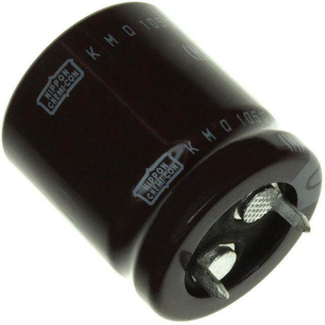
| 产品图片 |
|
| rohs | 符合RoHS无铅 / 符合限制有害物质指令(RoHS)规范要求 |
| 产品系列 | 晶体管,MOSFET,IXYS IXFH340N075T2TrenchT2™ HiPerFET™ |
| 数据手册 | |
| 产品型号 | IXFH340N075T2 |
| Pd-PowerDissipation | 935 W |
| Pd-功率耗散 | 935 W |
| Qg-GateCharge | 300 nC |
| Qg-栅极电荷 | 300 nC |
| RdsOn-Drain-SourceResistance | 3.2 mOhms |
| RdsOn-漏源导通电阻 | 3.2 mOhms |
| Vds-Drain-SourceBreakdownVoltage | 75 V |
| Vds-漏源极击穿电压 | 75 V |
| Vgs-Gate-SourceBreakdownVoltage | +/- 20 V |
| Vgs-栅源极击穿电压 | 20 V |
| Vgsth-Gate-SourceThresholdVoltage | 4 V |
| Vgsth-栅源极阈值电压 | 4 V |
| 上升时间 | 50 ns |
| 下降时间 | 35 ns |
| 不同Id时的Vgs(th)(最大值) | 4V @ 3mA |
| 不同Vds时的输入电容(Ciss) | 19000pF @ 25V |
| 不同Vgs时的栅极电荷(Qg) | 300nC @ 10V |
| 不同 Id、Vgs时的 RdsOn(最大值) | 3.2 毫欧 @ 100A,10V |
| 产品种类 | MOSFET |
| 供应商器件封装 | TO-247AD (IXFH) |
| 典型关闭延迟时间 | 60 ns |
| 功率-最大值 | 935W |
| 包装 | 管件 |
| 商标 | IXYS |
| 商标名 | HiPerFET |
| 安装类型 | 通孔 |
| 安装风格 | Through Hole |
| 封装 | Tube |
| 封装/外壳 | TO-247-3 |
| 封装/箱体 | TO-247-3 |
| 工厂包装数量 | 30 |
| 晶体管极性 | N-Channel |
| 最大工作温度 | + 175 C |
| 最小工作温度 | - 55 C |
| 标准包装 | 30 |
| 正向跨导-最小值 | 65 S |
| 漏源极电压(Vdss) | 75V |
| 电流-连续漏极(Id)(25°C时) | 340A (Tc) |
| 系列 | IXFH340N075 |
| 通道模式 | Enhancement |
| 配置 | Single |


- 商务部:美国ITC正式对集成电路等产品启动337调查
- 曝三星4nm工艺存在良率问题 高通将骁龙8 Gen1或转产台积电
- 太阳诱电将投资9.5亿元在常州建新厂生产MLCC 预计2023年完工
- 英特尔发布欧洲新工厂建设计划 深化IDM 2.0 战略
- 台积电先进制程称霸业界 有大客户加持明年业绩稳了
- 达到5530亿美元!SIA预计今年全球半导体销售额将创下新高
- 英特尔拟将自动驾驶子公司Mobileye上市 估值或超500亿美元
- 三星加码芯片和SET,合并消费电子和移动部门,撤换高东真等 CEO
- 三星电子宣布重大人事变动 还合并消费电子和移动部门
- 海关总署:前11个月进口集成电路产品价值2.52万亿元 增长14.8%


PDF Datasheet 数据手册内容提取
Advance Technical Information TrenchT2TM HiPerFETTM IXFH340N075T2 V = 75V DSS Power MOSFET IXFT340N075T2 I = 340A D25 R ≤≤≤≤≤ 3.2mΩΩΩΩΩ DS(on) N-Channel Enhancement Mode Avalanche Rated Fast Intrinsic Diode TO-247 (IXFH) G Symbol Test Conditions Maximum Ratings D D (TAB) S V T = 25°C to 175°C 75 V DSS J V T = 25°C to 175°C, R = 1MΩ 75 V DGR J GS V Transient ± 20 V GSM TO-268 (IXFT) I T = 25°C (Chip Capability) 340 A D25 C I Lead Current Limit, RMS 160 A LRMS G I T = 25°C, Pulse Width Limited by T 850 A DM C JM S I T = 25°C 170 A A C D (TAB) E T = 25°C 960 mJ AS C P T = 25°C 935 W D C G = Gate D = Drain T -55 ... +175 °C S = Source TAB = Drain J T 175 °C JM T -55 ... +175 °C stg Features T 1.6mm (0.062in.) from Case for 10s 300 °C L T Plastic Body for 10 seconds 260 °C sold (cid:122)International Standard Packages M Mounting Torque (TO-247) 1.13 / 10 Nm/lb.in. (cid:122)175°C Operating Temperature d (cid:122)High Current Handling Capability Weight TO-247 6 g TO-268 4 g (cid:122)Avalanche Rated (cid:122) Fast Intrinsic Diode (cid:122) Low R DS(on) Symbol Test Conditions Characteristic Values Advantages (T = 25°C Unless Otherwise Specified) Min. Typ. Max. J (cid:122) Easy to Mount BV V = 0V, I = 1mA 75 V DSS GS D (cid:122) Space Savings V V = V , I = 3mA 2.0 4.0 V (cid:122) High Power Density GS(th) DS GS D I V = ± 20V, V = 0V ±200 nA GSS GS DS Applications I V = V , V = 0V 25 μA DSS DS DSS GS TJ = 150°C 1.5 mA (cid:122) DC/DC Converters and Off-line UPS R V = 10V, I = 100A, Note 1 3.2 mΩ (cid:122) Primary- Side Switch DS(on) GS D (cid:122) High Current Switching Applications © 2009 IXYS CORPORATION, All Rights Reserved DS100194(9/09)
IXFH340N075T2 IXFT340N075T2 Symbol Test Conditions Characteristic Values TO-247 (IXFH) Outline (T = 25°C, Unless Otherwise Specified) Min. Typ. Max. J g V = 10V, I = 60A, Note 1 65 110 S fs DS D C 19 nF iss C V = 0V, V = 25V, f = 1MHz 2230 pF ∅ P oss GS DS 1 2 3 C 490 pF rss R Gate Input Resistance 1.7 Ω Gi t 26 ns d(on) Resistive Switching Times t 50 ns r V = 10V, V = 0.5 • V , I = 100A e GS DS DSS D t R = 1 Ω ( E x te r n a l ) 60 ns Terminals: 1 - Gate 2 - Drain d(off) G 3 - Source Tab - Drain t 35 ns f Dim. Millimeter Inches Q 300 nC Min. Max. Min. Max. g(on) A 4.7 5.3 .185 .209 Q V = 10V, V = 0.5 • V , I = 0.5 • I 68 nC gs GS DS DSS D D25 A1 2.2 2.54 .087 .102 A 2.2 2.6 .059 .098 Q 70 nC 2 gd b 1.0 1.4 .040 .055 R 0.16 °C/W b1 1.65 2.13 .065 .084 thJC b 2.87 3.12 .113 .123 2 R TO-247 0.21 °C/W C .4 .8 .016 .031 thCH D 20.80 21.46 .819 .845 E 15.75 16.26 .610 .640 e 5.20 5.72 0.205 0.225 Source-Drain Diode L 19.81 20.32 .780 .800 L1 4.50 .177 Symbol Test Conditions Characteristic Values ∅P 3.55 3.65 .140 .144 (T = 25°C, Unless Otherwise Specified) Min. Typ. Max. J Q 5.89 6.40 0.232 0.252 I V = 0V 340 A R 4.32 5.49 .170 .216 S GS S 6.15 BSC 242 BSC I Repetitive, Pulse Width Limited by T 1360 A SM JM TO-268 (IXFT) Outline V I = 100A, V = 0V, Note 1 1.3 V SD F GS t I = 1 7 0 A , V = 0 V 75 ns rr F GS I -di/dt = 100A/μs 4.4 A RM Q V = 37.5V 165 nC RM R Note 1. Pulse test, t ≤ 300μs; duty cycle, d ≤ 2%. Terminals: 1 - Gate 2 - Drain 3 - Source Tab - Drain ADVANCE TECHNICAL INFORMATION The product presented herein is under development. The Technical Specifications offered are derived from a subjective evaluation of the design, based upon prior knowledge and experience, and constitute a "considered reflection" of the anticipated result. IXYS reserves the right to change limits, test conditions, and dimensions without notice. IXYS Reserves the Right to Change Limits, Test Conditions, and Dimensions. IXYS MOSFETs and IGBTs are covered 4,835,592 4,931,844 5,049,961 5,237,481 6,162,665 6,404,065 B1 6,683,344 6,727,585 7,005,734 B2 7,157,338B2 by one or more of the following U.S. patents:4,850,072 5,017,508 5,063,307 5,381,025 6,259,123 B1 6,534,343 6,710,405 B2 6,759,692 7,063,975 B2 4,881,106 5,034,796 5,187,117 5,486,715 6,306,728 B1 6,583,505 6,710,463 6,771,478 B27,071,537
IXFH340N075T2 IXFT340N075T2 Fig. 1. Output Characteristics Fig. 2. Extended Output Characteristics @ T = 25ºC @ T = 25ºC J J 350 400 VGS = 15V VGS = 15V 300 10V 350 10V 9V 8V 7V 8V 300 250 7V s s250 pere200 6V pere 6V m m200 A A I - D150 I - D150 5V 5V 100 100 50 50 4V 4V 0 0 0.0 0.1 0.2 0.3 0.4 0.5 0.6 0.7 0.8 0.9 1.0 0.0 0.5 1.0 1.5 2.0 2.5 3.0 3.5 4.0 4.5 VDS - Volts VDS - Volts Fig. 3. Output Characteristics Fig. 4. R Normalized to I = 170A Value vs. DS(on) D @ TJ = 150ºC Junction Temperature 350 2.4 V G S = 1150VV 2.2 VGS = 10V 300 9V 8V 2.0 7V 250 ed1.8 I D = 340A z eres200 6V mali1.6 mp Nor I D = 170A I - AD110500 5V R - DS(on)11..24 1.0 50 0.8 4V 0 0.6 0.0 0.2 0.4 0.6 0.8 1.0 1.2 1.4 1.6 1.8 2.0 -50 -25 0 25 50 75 100 125 150 175 VDS - Volts TJ - Degrees Centigrade Fig. 5. R Normalized to I = 170A Value vs. DS(on) D Fig. 6. Drain Current vs. Case Temperature Drain Current 2.4 180 External Lead Current Limit 2.2 160 2.0 TJ = 175ºC 140 d ze 1.8 120 ormali 1.6 VGS = 10V peres100 N 15V - - - - - m - on) 1.4 - AD 80 S( I D 1.2 60 R TJ = 25ºC 1.0 40 0.8 20 0.6 0 0 40 80 120 160 200 240 280 320 360 -50 -25 0 25 50 75 100 125 150 175 ID - Amperes TC - Degrees Centigrade © 2009 IXYS CORPORATION, All Rights Reserved
IXFH340N075T2 IXFT340N075T2 Fig. 7. Input Admittance Fig. 8. Transconductance 200 240 TJ = - 40ºC 180 200 160 140 25ºC 160 s es120 en er m mp100 Sie120 150ºC I - AD 80 TJ = 150ºC g - f s 25ºC 80 60 - 40ºC 40 40 20 0 0 2.5 3.0 3.5 4.0 4.5 5.0 5.5 0 20 40 60 80 100 120 140 160 180 200 220 VGS - Volts ID - Amperes Fig. 9. Forward Voltage Drop of Intrinsic Diode Fig. 10. Gate Charge 10 300 9 VDS = 37.5V 250 8 I D = 170A I G = 10mA 7 200 eres olts 6 p V Am150 - S 5 - S VG 4 I100 TJ = 150ºC 3 TJ = 25ºC 2 50 1 0 0 0.3 0.4 0.5 0.6 0.7 0.8 0.9 1.0 1.1 1.2 1.3 1.4 0 50 100 150 200 250 300 VSD - Volts QG - NanoCoulombs Fig. 11. Capacitance Fig. 12. Forward-Bias Safe Operating Area 100,000 1,000 f = 1 MHz RDS(on) Limit s 25µs d ara10,000 Ciss 100 External Lead Current Limit 100µs oF es e - Pic Amper acitanc 1,000 Coss I - D 10 100ms DC 1ms p a C TJ = 175ºC 10ms Crss TC = 25ºC Single Pulse 100 1 0 5 10 15 20 25 30 35 40 1 10 100 VDS - Volts VDS - Volts IXYS Reserves the Right to Change Limits, Test Conditions, and Dimensions. IXYS REF: F_340N075T2(V8)9-15-09
IXFH340N075T2 IXFT340N075T2 Fig. 13. Resistive Turn-on Fig. 14. Resistive Turn-on Rise Time vs. Junction Temperature Rise Time vs. Drain Current 70 70 RG = 1Ω , VGS = 10V RG = 1Ω , VGS = 10V 65 VDS = 37.5V 65 VDS = 37.5V TJ = 125ºC ds 60 ds 60 n n co I D = 200A co e e os 55 os 55 n n a a N N t - r 50 I D = 100A t - r 50 TJ = 25ºC 45 45 40 40 25 35 45 55 65 75 85 95 105 115 125 100 110 120 130 140 150 160 170 180 190 200 TJ - Degrees Centigrade ID - Amperes Fig. 15. Resistive Turn-on Fig. 16. Resistive Turn-off Switching Times vs. Gate Resistance Switching Times vs. Junction Temperature 400 90 50 90 350 t r td(on) - - - - 80 45 t f td(off) - - - - 85 noseconds223050000 TVJD S= =1 2357º.C5 V, V G S = 10V I D = 200A 567000 d(on) - Nanot noseconds 334050 RVDGS = = 1 3Ω7 .,5 VVG S I= D 1 =0 V100A, 200A 778050 d(off) - Nant t - Nar 150 I D = 100A 40 second t - Naf 25 65 osecon 100 30 s 20 60 ds 50 20 15 55 0 10 10 50 1 2 3 4 5 6 7 8 9 10 11 12 13 14 15 25 35 45 55 65 75 85 95 105 115 125 RG - Ohms TJ - Degrees Centigrade Fig. 17. Resistive Turn-off Fig. 18. Resistive Turn-off Switching Times vs. Drain Current Switching Times vs. Gate Resistance 48 85 500 400 t f td(off) - - - - 450 t f td(off) - - - - 360 44 80 RG = 1Ω , VGS = 10V 400 TJ = 125ºC , VGS = 10V 320 econds3460 VDS = 37.5V 7705 d(off) - Nt econds 330500 VDS = 37.5V 224800 d(off) - Nt t - Nanosf 2382 TJ = 25ºC, 125ºC 6605 anoseconds t - Nanosf 122505000 I D = 200A I D = 100A 112260000 anoseconds 100 80 24 55 50 40 20 50 0 0 100 110 120 130 140 150 160 170 180 190 200 1 2 3 4 5 6 7 8 9 10 11 12 13 14 15 ID - Amperes RG - Ohms © 2009 IXYS CORPORATION, All Rights Reserved
IXFH340N075T2 IXFT340N075T2 Fig. 19. Maximum Transient Thermal Impedance 1.00 Fig. 19. Maximum Transient Thermal Impedance afaf 0.20 0.10 W C / - ºC h)J Z(t 0.01 0.0001 0.001 0.01 0.1 1 10 Pulse Width - Seconds IXYS Reserves the Right to Change Limits, Test Conditions, and Dimensions. IXYS REF: F_340N075T2(V8)9-15-09
Disclaimer Notice - Information furnished is believed to be accurate and reliable. However, users should independently evaluate the suitability of and test each product selected for their own applications. Littelfuse products are not designed for, and may not be used in, all applications. Read complete Disclaimer Notice at www.littelfuse.com/disclaimer-electronics.