ICGOO在线商城 > 集成电路(IC) > 接口 - 模拟开关,多路复用器,多路分解器 > BU4053BCFV-E2
 Datasheet下载
- 型号: BU4053BCFV-E2
- 制造商: ROHM Semiconductor
- 库位|库存: xxxx|xxxx
- 要求:
| 数量阶梯 | 香港交货 | 国内含税 |
| +xxxx | $xxxx | ¥xxxx |
查看当月历史价格
查看今年历史价格
BU4053BCFV-E2产品简介:
ICGOO电子元器件商城为您提供BU4053BCFV-E2由ROHM Semiconductor设计生产,在icgoo商城现货销售,并且可以通过原厂、代理商等渠道进行代购。 BU4053BCFV-E2价格参考¥18.03-¥18.03。ROHM SemiconductorBU4053BCFV-E2封装/规格:接口 - 模拟开关,多路复用器,多路分解器, 3 Circuit IC Switch 2:1 160 Ohm 16-SSOPB。您可以下载BU4053BCFV-E2参考资料、Datasheet数据手册功能说明书,资料中有BU4053BCFV-E2 详细功能的应用电路图电压和使用方法及教程。
BU4053BCFV-E2 是由罗姆半导体(Rohm Semiconductor)生产的一款模拟开关,属于接口类元件中的模拟开关、多路复用器和多路分解器类别。以下是该型号的一些典型应用场景:

 1. 音频信号切换
   - BU4053BCFV-E2 可用于音频设备中实现多路音频信号的切换。例如,在音响系统或耳机放大器中,可以通过该芯片选择不同的输入源(如麦克风、线路输入或蓝牙模块),从而实现灵活的音频信号管理。

 2. 传感器信号切换
   - 在工业自动化或物联网设备中,该芯片可用于切换多个传感器的信号输入。例如,温度传感器、压力传感器或湿度传感器可以共用一个 ADC 输入通道,通过多路复用功能依次读取各个传感器的数据。

 3. 通信接口切换
   - 在多协议通信场景中,BU4053BCFV-E2 可以用来切换不同的通信接口(如 UART、SPI 或 I2C)。这在需要动态切换通信链路的嵌入式系统中非常有用,例如在智能仪表或手持设备中。

 4. 显示信号控制
   - 在小型显示屏或多屏显示系统中,该芯片可以用于切换不同来源的视频信号。例如,OLED 或 LCD 显示屏可能需要从主控制器或备用控制器接收数据,BU4053BCFV-E2 能够实现信号路径的快速切换。

 5. 电池管理系统
   - 在电池管理系统(BMS)中,BU4053BCFV-E2 可用于监测多节电池的电压或电流信号。通过多路复用功能,可以依次测量每节电池的状态,从而优化电池的充放电管理。

 6. 医疗设备信号处理
   - 在便携式医疗设备(如心率监测仪或血糖仪)中,该芯片可以用于切换生物信号的采集通道。例如,它可以将来自多个电极的信号逐一传递到信号处理单元。

 特点与优势:
- 低导通电阻:确保信号传输过程中失真最小。
- 宽工作电压范围:适用于多种电源环境。
- 高可靠性:适合对稳定性要求较高的应用场合。
- 小封装尺寸:便于在空间受限的设计中使用。

综上所述,BU4053BCFV-E2 适用于需要多路信号切换和高效信号管理的各种电子系统,尤其是在消费电子、工业控制和医疗设备领域具有广泛的应用前景。
| 参数 | 数值 |
| 产品目录 | 集成电路 (IC)半导体 |
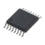
| 描述 | IC MUX/DEMUX TRIPLE 2X1 16SSOP多路器开关 IC TRIPLE 2 CH ANALOG MULTIPLEXER |
| 产品分类 | |
| 品牌 | Rohm Semiconductor |
| 产品手册 | |
| 产品图片 |
|
| rohs | 符合RoHS无铅 / 符合限制有害物质指令(RoHS)规范要求 |
| 产品系列 | 开关 IC,多路器开关 IC,ROHM Semiconductor BU4053BCFV-E24000B |
| 数据手册 | |
| 产品型号 | BU4053BCFV-E2 |
| 产品种类 | 多路器开关 IC |
| 传播延迟时间 | 45 ns, 20 ns, 15 ns |
| 供应商器件封装 | 16-SSOPB |
| 其它名称 | BU4053BCFV-E2CT |
| 功能 | 多路复用器/多路分解器 |
| 包装 | 剪切带 (CT) |
| 商标 | ROHM Semiconductor |
| 安装类型 | 表面贴装 |
| 安装风格 | SMD/SMT |
| 导通电阻 | 160 欧姆 |
| 导通电阻—最大值 | 950 Ohms |
| 封装 | Reel |
| 封装/外壳 | 16-TSSOP(0.173",4.40mm 宽) |
| 封装/箱体 | SSOP-B-16 |
| 工作温度 | -40°C ~ 85°C |
| 工作电源电压 | 3 V to 18 V |
| 工作电源电流 | 5 uA |
| 工厂包装数量 | 2500 |
| 带宽 | 20 MHz |
| 开关数量 | 3 |
| 最大功率耗散 | 620 mW |
| 最大工作温度 | + 85 C |
| 最小工作温度 | - 40 C |
| 标准包装 | 1 |
| 电压-电源,单/双 (±) | 3 V ~ 18 V |
| 电压源 | 单电源 |
| 电流-电源 | 15µA |
| 电路 | 3 x 2:1 |
| 空闲时间—最大值 | 550 ns |
| 运行时间—最大值 | 550 ns |
| 通道数量 | 3 Channel |


- 商务部:美国ITC正式对集成电路等产品启动337调查
- 曝三星4nm工艺存在良率问题 高通将骁龙8 Gen1或转产台积电
- 太阳诱电将投资9.5亿元在常州建新厂生产MLCC 预计2023年完工
- 英特尔发布欧洲新工厂建设计划 深化IDM 2.0 战略
- 台积电先进制程称霸业界 有大客户加持明年业绩稳了
- 达到5530亿美元!SIA预计今年全球半导体销售额将创下新高
- 英特尔拟将自动驾驶子公司Mobileye上市 估值或超500亿美元
- 三星加码芯片和SET,合并消费电子和移动部门,撤换高东真等 CEO
- 三星电子宣布重大人事变动 还合并消费电子和移动部门
- 海关总署:前11个月进口集成电路产品价值2.52万亿元 增长14.8%


PDF Datasheet 数据手册内容提取
Datasheet General Purpose CMOS Logic IC Triple 2ch Analog Multiplexer/Dem ultiplexer BU4053BC BU4053BCF BU4053BCFV General Description Key Specifications The BU4053BC, BU4053BCF, BU4053BCFV are Operating Supply Voltage Range: 3V to 18V multiplexers/demultiplexers with capabilities of selection and mixture of analog signal and digital signal. Input Voltage Range: V to V SS DD This series are configured with triple 2 channels Operating Temperature Range: -40°C to +85°C input/output. The digital signal of the control terminal turns on the corresponding switch of each channel. The large Packages W(Typ) x D(Typ) x H(Max) amplitude voltage (VDD-VEE) can be switched by the DIP16 19.40mm x 6.50mm x 7.95mm control signal with small logical amplitude voltage SOP16 10.00mm x 6.20mm x 1.71mm (VDD-VSS). SSOP-B16 5.00mm x 6.40mm x 1.35mm Features Low power consumption Wide operating supply voltage High input impedance DIP16 SOP16 SSOP-B16 Truth Table CONTROL ON SWITCH INHIBIT A B C L L L L X0,Y0,Z0 L H L L X1,Y0,Z0 L L H L X0,Y1,Z0 L H H L X1,Y1,Z0 L L L H X0,Y0,Z1 L H L H X1,Y0,Z1 L L H H X0,Y1,Z1 L H H H X1,Y1,Z1 H Don’t Care Don’t Care Don’t Care NONE 〇Product structure : Silicon monolithic integrated circuit 〇This product has no designed protection against radioactive rays .w ww.rohm.com TSZ02201-0RDR0GZ00300-1-2 © 2015 ROHM Co., Ltd. All rights reserved. 1/17 TSZ22111 • 14 • 001 08.Jan.2015 Rev.001
BU4053BC BU4053BCF BU4053BCFV Pin Configuration (TOP VIEW) Y1 1 16 VDD Y0 2 15 Y Z1 3 14 X Z 4 13 X1 Z0 5 12 X0 INHIBIT 6 11 A VEE 7 10 B VSS 8 9 C Pin Description Pin No. Pin Name I/O Function 1 Y 1 I/O Analog Switch Input / Output 2 Y0 I/O Analog Switch Input / Output 3 Z1 I/O Analog Switch Input / Output 4 Z I/O Analog Switch Input / Output 5 Z0 I/O Analog Switch Input / Output 6 INHIBIT I Control Input 7 VEE ― Power Supply(-) 8 VSS ― Power Supply(-) 9 C I Control Input 10 B I Control Input 11 A I Control Input 12 X0 I/O Analog Switch Input / Output 13 X1 I/O Analog Switch Input / Output 14 X I/O Analog Switch Input / Output 15 Y I/O Analog Switch Input / Output 16 VDD ― Power Supply (+) www.rohm.com TSZ02201-0RDR0GZ00300-1-2 © 2014 ROHM Co., Ltd. All rights reserved. 2/17 TSZ22111 • 15 • 001 08.Jan.2015 Rev.001
BU4053BC BU4053BCF BU4053BCFV Block Diagram VDD INHIBIT A LEVEL BINARY TO 1 OF 2 DECODER B CONVERTER WITH INHIBIT C VSS VEE X0 X X1 Y0 Y Y1 Z0 Z Z1 Absolute Maximum Ratings (T =25°C) A Parameter Symbol Rating Unit Supply Voltage (Note 1) VDD -0.5 to +20.0 V Control Input Voltage VCIN (VSS-0.5) ~ (VDD+0.5) V Analog Switch Input/Output Voltage VIN / VOUT (VEE-0.5) ~ (VDD+0.5) V Control Input Current ICIN ±10 mA Operating Temperature Topr -40 to +85 °C Storage Temperature Tstg -55 to +150 °C Maximum Junction Temperature TJmax +150 °C DIP16 1.25 (Note 2) Power Dissipation PD SOP16 0.62 (Note 3) W SSOP-B16 0.87 (Note 4) (Note 1) It Contain voltage of VSS to VDD and Voltage of VEE to VDD. It shoud be VEE ≤ VSS (Note 2) Mounted on 70mm x 70mm x 1.6mm glass epoxy board. Reduce 10.0mW per 1°C above 25°C (Note 3) Mounted on 70mm x 70mm x 1.6mm glass epoxy board. Reduce 5.0mW per 1°C above 25°C (Note 4) Mounted on 70mm x 70mm x 1.6mm glass epoxy board. Reduce 7.0mW per 1°C above 25°C Caution: Operating the IC over the absolute maximum ratings may damage the IC. The damage can either be a short circuit between pins or an open circuit between pins and the internal circuitry. Therefore, it is important to consider circuit protection measures, such as adding a fuse, in case the IC is operated over the absolute maximum ratings. Recommended Operating Conditions (T = -40°C to +85°C) A Parameter Symbol Min Typ Max Unit Supply Voltage V 3.0 - 18 V DD Control Input Voltage V V - V V CIN SS DD Analog Switch Input/Output Voltage V / V V - V V IN OUT EE DD www.rohm.com TSZ02201-0RDR0GZ00300-1-2 © 2014 ROHM Co., Ltd. All rights reserved. 3/17 TSZ22111 • 15 • 001 08.Jan.2015 Rev.001
BU4053BC BU4053BCF BU4053BCFV Electrical Characteristics (Unless otherwise specified V =V =0V, T =25°C) EE SS A Parameter Symbol Min Typ Max Unit Conditions DC Characteristics 3.5 - - V =5V DD Input “H” voltage V 7.0 - - V V =10V - IH DD 11.0 - - V =15V DD - - 1.5 V =5V DD Input “L” voltage V - - 3.0 V V =10V - IL DD - - 4.0 V =15V DD Input “H” current I - - 0.3 uA V =15V V =15V IH DD IH Input “L” current I - - -0.3 uA V =15V V =0V IL DD IL - - 950 V =5V DD ON resistance R - - 250 Ω V =10V - ON DD - - 160 V =15V DD - 10 - V =5V DD ON resistance defluxion △RON - 6 - Ω VDD=10V - - 4 - V =15V DD - - 0.3 V =15V - DD Channel-OFF Leakage current I µA OFF - - -0.3 V =15V - DD - - 5 V =5V DD Quiescent supply current I - - 10 µA V =10V DD DD V =V or V IN DD EE - - 15 V =15V DD Switching Characteristics, C =50pF L - 15 45 V =5V DD Propagation delay time tPLH - 8 20 ns V =10V - IN→OUT tPHL DD - 6 15 V =15V DD - 170 550 V =5V DD Propagation delay time t ,t PHZ PLZ - 90 240 ns V =10V - CONTROL (A,B,C)→OUT t ,t DD PZH PZL - 70 160 V =15V DD - 150 380 V =5V DD Propagation delay time t ,t PHZ PLZ - 70 200 ns V =10V - CONTROL (INHIBIT)→OUT t ,t DD PZH PZL - 50 160 V =15V DD Maximum propagation frequency f - 20 - MHz V =5V V =-5V MAX DD EE Feed through attenuation F - 0.7 - MHz V =5V V =-5V T DD EE Sine wave distortion D - 0.02 - % V =5V V =-5V DD EE Input capacitance (control input) C - 5 - pF - - C Input capacitance (switch input) C - 10 - pF - - S www.rohm.com TSZ02201-0RDR0GZ00300-1-2 © 2014 ROHM Co., Ltd. All rights reserved. 4/17 TSZ22111 • 15 • 001 08.Jan.2015 Rev.001
BU4053BC BU4053BCF BU4053BCFV Waveforms of Switching Characteristics X0~X1 VDD CONTROL VDD Y0~Y1 50% Z0~Z1 A (INPUT) VEE B OUT C X/Y/Z 50% INHIBIT X / Y / Z (OUTPUT) X0 to X1 RL CL Y 0 to Y1 Z 0 to Z1 tPLH tPHL IN VEE, VSS Figure 1. Propagation Delay Time Figure 2. Test Circuit 1 (tPLH,tPHL) (IN→OUT) (t ,t ) PLH PHL VDD CONTROL VDD CONTROL 50% A (INPUT) VSS B OUT C X/Y/Z X / Y / Z 90% (OUTPUT) 50% INHIBIT (A,B,C,I X0 to X1 RL CL Y 0 to Y1 NHIBIT) VDD Z 0 to Z1 →(tPOLHU,tPTH)L tPZH tPHZ VEE, VSS ) T Figure 3. Propagation Delay Time Figure 4. Test Circuit 2 (t ,t ) PZH PHZ (CONTROL (A,B,C,INHIBIT)→OUT) (tPLH,tPHL) VDD CONTROL VDD CONTROL (INPUT) 50% A RL CL VSS B OUT C X/Y/Z 50% INHIBIT X / Y / Z (OUTPUT) 10% X0 to X1 Y 0 to Y1 Z 0 to Z1 tPZL tPLZ VEE, VSS Figure 5. Propagation Delay Time Figure 6. Test Circuit 3 (t ,t ) PZL PLZ (CONTROL (A,B,C,INHIBIT)→OUT) (t ,t ) PZL PLZ www.rohm.com TSZ02201-0RDR0GZ00300-1-2 © 2014 ROHM Co., Ltd. All rights reserved. 5/17 TSZ22111 • 15 • 001 08.Jan.2015 Rev.001
BU4053BC BU4053BCF BU4053BCFV Typical Performance Curves 1400 1400 1200 1200 1000 1000 Ω] Ω] e [ e [ nc 800 nc 800 a a Resist 600 Resist 600 85°C N N 25°C O 400 85°C O 400 -40°C 25°C -40°C 200 200 0 0 0 1 2 3 4 5 0 1 2 3 4 5 Input Voltage [V] Input Voltage [V] Figure 7. ON R e s i s ta n c e vs Input Voltage Figure 8. ON Resistance vs Input Voltage VDD=3V V D D =5V 1400 1400 1200 1200 1000 1000 Ω] Ω] e [ e [ c 800 c 800 n n a a st st esi 600 esi 600 R R N N O O 400 400 85°C 85°C 25°C 25°C -40°C -40°C 200 200 0 0 0 2 4 6 8 10 0 3 6 9 12 15 Input Voltage [V] Input Voltage [V] Figure 9. ON Resistance vs Input Voltage Figure 10. ON Resistance vs Input Voltage VDD=10V V D D = 1 5V www.rohm.com TSZ02201-0RDR0GZ00300-1-2 © 2014 ROHM Co., Ltd. All rights reserved. 6/17 TSZ22111 • 15 • 001 08.Jan.2015 Rev.001
BU4053BC BU4053BCF BU4053BCFV Typical Performance Curves - continued 50 50 Operating Temperature Range Operating Temperature Range s]40 40 n e [ m s] y Ti30 y [n30 a n n Del VDD=3V gatio VDD=3V o a ati20 op20 ag VDD=5V Pr VDD=5V p Pro10 VDD=10V 10 VDD=10V VDD=18V VDD=18V 0 0 -50 -25 0 25 50 75 100 -50 -25 0 25 50 75 100 Ambient Temperature [°C] Ambient Temperature [°C] Figure 11. Propagation Delay Time tPLH (IN→OUT) vs Figure 12. Propagation Delay Time tPHL (IN→OUT) vs Ambie n t T e m perature Ambient Temperature 500 500 Operating Temperature Range Operating Temperature Range e [ns]400 VDD=3V e [ns] 400 VDD=3V m m ay Ti300 ay Ti 300 el el n D VDD=5V n D VDD=5V atio200 VDD=10V atio 200 VDD=10V g g a a p p Pro100 VDD=18V Pro 100 VDD=18V 0 0 -50 -25 0 25 50 75 100 -50 -25 0 25 50 75 100 Ambient Temperature [°C] Ambient Temperature [°C] Figure 13. Propagation Delay Time tPZH Figure 14. Propagation Delay Time tPHZ (CONTROL (A,B,C)→OUT) vs Ambient Temperature (CONTROL (A,B,C)→OUT) vs Ambient Temperature www.rohm.com TSZ02201-0RDR0GZ00300-1-2 © 2014 ROHM Co., Ltd. All rights reserved. 7/17 TSZ22111 • 15 • 001 08.Jan.2015 Rev.001
BU4053BC BU4053BCF BU4053BCFV Typical Performance Curves - continued 500 500 Operating Temperature Range Operating Temperature Range 400 400 s] s] n n e [ e [ m m y Ti300 VDD=3V y Ti300 a a el el n D n D VDD=3V o200 VDD=5V o200 ati ati ag VDD=10V ag p p o o VDD=5V Pr100 VDD=18V Pr100 VDD=10V VDD=18V 0 0 -50 -25 0 25 50 75 100 -50 -25 0 25 50 75 100 Ambient Temperature [°C] Ambient Temperature [°C] Figure 15. Propagation Delay Time t Figure 16. Propagation Delay Time t PLZ PZL (CONTROL (A,B,C)→OUT) vs Ambient Temperature (CONTROL (A,B,C)→O UT) vs Ambient Temperature 500 500 Operating Temperature Range Operating Temperature Range 400 400 s] s] e [n e [n VDD=3V m m y Ti300 y Ti 300 a a n Del VDD=3V n Del VDD=5V atio200 atio 200 VDD=10V g g a a op VDD=5V op VDD=18V Pr100 Pr 100 VDD=10V VDD=18V 0 0 -50 -25 0 25 50 75 100 -50 -25 0 25 50 75 100 Ambient Temperature [°C] Ambient Temperature [°C] Figure 17. Propagation Delay Time t Figure 18. Propagation Delay Time t PZH PHZ (CONTROL (INHIBIT)→OUT) vs Ambient Temperature (CONTROL (INHIBIT)→OUT) vs Ambient Temperature www.rohm.com TSZ02201-0RDR0GZ00300-1-2 © 2014 ROHM Co., Ltd. All rights reserved. 8/17 TSZ22111 • 15 • 001 08.Jan.2015 Rev.001
BU4053BC BU4053BCF BU4053BCFV Typical Performance Curves - continued 500 500 Operating Temperature Range Operating Temperature Range 400 400 s] s] n n e [ e [ m m y Ti 300 VDD=3V y Ti 300 a a el el on D 200 VDD=5V on D 200 VDD=3V ati ati ag VDD=10V ag p p Pro 100 VDD=18V Pro 100 VDD=5V VDD=10V VDD=18V 0 0 -50 -25 0 25 50 75 100 -50 -25 0 25 50 75 100 Ambient Temperature [°C] Ambient Temperature [°C] Figure 19. Propagation Delay Time t Figure 20. Propagation Delay Time t PZL PLZ (CONTROL (INHIBIT)→OUT) vs Ambient Temperature (CONTROL (INHIBIT)→OUT) vs Ambient Temperature www.rohm.com TSZ02201-0RDR0GZ00300-1-2 © 2015 ROHM Co., Ltd. All rights reserved. 9/17 TSZ22111 • 15 • 001 08.Jan.2015 Rev.001
BU4053BC BU4053BCF BU4053BCFV Power Dissipation Power dissipation (total loss) indicates the power that can be consumed by IC at T =25°C(normal temperature). IC is A heated when it consumed power, and the temperature of IC chip becomes higher than ambient temperature. The temperature that can be accepted by IC chip depends on circuit configuration, manufacturing process, and consumable power is limited. Power dissipation is determined by the temperature allowed in IC chip(maximum junction temperature) and thermal resistance of package(heat dissipation capability). The maximum junction temperature is typically equal to the maximum value in the storage temperature range. Heat generated by consumed power of IC radiates from the mold resin or lead frame of the package. The parameter which indicates this heat dissipation capability(hardness of heat release)is called thermal resistance, represented by the symbol θ (°C/W).The temperature of IC inside the package can be JA estimated by this thermal resistance. Figure 21 shows the model of thermal resistance of the package. Thermal resistance θ , ambient temperature T , maximum junction temperature T , and power dissipation P can be calculated by the JA A Jmax D equation below: θ = (T - T ) / P (°C/W) JA Jmax A D Derating curve in Figure 22 indicates power that can be consumed by IC with reference to ambient temperature. Power that can be consumed by IC begins to attenuate at certain ambient temperature. This gradient is determined by thermal resistance θ . Thermal resistance θ depends on chip size, power consumption, package, ambient temperature, package JA JA condition, wind velocity, etc even when the same of package is used. Thermal reduction curve indicates a reference value measured at a specified condition. 1.6 1.4 BU4053BC (DIP16) 1.2 W] n [ 1.0 BU4053BCFV (SSOP-B16) o ati p 0.8 si s Di θJA =( TJmax - TA)/ PD (°C/W) er 0.6 w o Ambie周nt囲 te温m度pe rTaat u[℃re] TA (℃) P 0.4 BU4053BCF (SOP16) 0.2 0.0 Chip suチrfッaプce表 te面m温p度er a Ttuj r[℃e T]J(℃) 0 25 50 75 85 100 125 150 消費電力 P [W] Ambient Temperature [℃] Figure 21. Thermal Resistance Figure 22. Derating Curve I/O Equivalent Circuits Control Input Terminals Input / Output Terminals Pin No. 6,9,10,11 1,2,3,4,5,12,13,14,15 VDD VDD VDD VDD VDD VDD Equivalence Circuit GND GND GND V SS VSS VEE www.rohm.com TSZ02201-0RDR0GZ00300-1-2 © 2015 ROHM Co., Ltd. All rights reserved. 10/17 TSZ22111 • 15 • 001 08.Jan.2015 Rev.001
BU4053BC BU4053BCF BU4053BCFV Operational Notes 1. Reverse Connection of Power Supply Connecting the power supply in reverse polarity can damage the IC. Take precautions against reverse polarity when connecting the power supply, such as mounting an external diode between the power supply and the IC’s power supply pins. 2. Power Supply Lines Design the PCB layout pattern to provide low impedance supply lines. Separate the ground and supply lines of the digital and analog blocks to prevent noise in the ground and supply lines of the digital block from affecting the analog block. Furthermore, connect a capacitor to ground at all power supply pins. Consider the effect of temperature and aging on the capacitance value when using electrolytic capacitors. 3. Ground Voltage Ensure that no pins are at a voltage below that of the ground pin at any time, even during transient condition. 4. Ground Wiring Pattern When using both small-signal and large-current ground traces, the two ground traces should be routed separately but connected to a single ground at the reference point of the application board to avoid fluctuations in the small-signal ground caused by large currents. Also ensure that the ground traces of external components do not cause variations on the ground voltage. The ground lines must be as short and thick as possible to reduce line impedance. 5. Thermal Consideration Should by any chance the power dissipation rating be exceeded the rise in temperature of the chip may result in deterioration of the properties of the chip. The absolute maximum rating of the Pd stated in this specification is when the IC is mounted on a 70mm x 70mm x 1.6mm glass epoxy board. In case of exceeding this absolute maximum rating, increase the board size and copper area to prevent exceeding the Pd rating. 6. Recommended Operating Conditions These conditions represent a range within which the expected characteristics of the IC can be approximately obtained. The electrical characteristics are guaranteed under the conditions of each parameter. 7. Inrush Current When power is first supplied to the IC, it is possible that the internal logic may be unstable and inrush current may flow instantaneously due to the internal powering sequence and delays, especially if the IC has more than one power supply. Therefore, give special consideration to power coupling capacitance, power wiring, width of ground wiring, and routing of connections. 8. Operation Under Strong Electromagnetic Field Operating the IC in the presence of a strong electromagnetic field may cause the IC to malfunction. 9. Testing on Application Boards When testing the IC on an application board, connecting a capacitor directly to a low-impedance output pin may subject the IC to stress. Always discharge capacitors completely after each process or step. The IC’s power supply should always be turned off completely before connecting or removing it from the test setup during the inspection process. To prevent damage from static discharge, ground the IC during assembly and use similar precautions during transport and storage. 10. Inter-pin Short and Mounting Errors Ensure that the direction and position are correct when mounting the IC on the PCB. Incorrect mounting may result in damaging the IC. Avoid nearby pins being shorted to each other especially to ground, power supply and output pin. Inter-pin shorts could be due to many reasons such as metal particles, water droplets (in very humid environment) and unintentional solder bridge deposited in between pins during assembly to name a few. www.rohm.com TSZ02201-0RDR0GZ00300-1-2 © 2015 ROHM Co., Ltd. All rights reserved. 11/17 TSZ22111 • 15 • 001 08.Jan.2015 Rev.001
BU4053BC BU4053BCF BU4053BCFV Operational Notes – continued 11. Unused Input Pins Input pins of an IC are often connected to the gate of a MOS transistor. The gate has extremely high impedance and extremely low capacitance. If left unconnected, the electric field from the outside can easily charge it. The small charge acquired in this way is enough to produce a significant effect on the conduction through the transistor and cause unexpected operation of the IC. So unless otherwise specified, unused input pins should be connected to the power supply or ground line. 12. Regarding the Input Pin of the IC In the construction of this IC, P-N junctions are inevitably formed creating parasitic diodes or transistors. The operation of these parasitic elements can result in mutual interference among circuits, operational faults, or physical damage. Therefore, conditions which cause these parasitic elements to operate, such as applying a voltage to an input pin lower than the ground voltage should be avoided. Furthermore, do not apply a voltage to the input pins when no power supply voltage is applied to the IC. Even if the power supply voltage is applied, make sure that the input pins have voltages within the values specified in the electrical characteristics of this IC. 13. Ceramic Capacitor When using a ceramic capacitor, determine the dielectric constant considering the change of capacitance with temperature and the decrease in nominal capacitance due to DC bias and others. 14. Area of Safe Operation (ASO) Operate the IC such that the output voltage, output current, and power dissipation are all within the Area of Safe Operation (ASO). www.rohm.com TSZ02201-0RDR0GZ00300-1-2 © 2015 ROHM Co., Ltd. All rights reserved. 12/17 TSZ22111 • 15 • 001 08.Jan.2015 Rev.001
BU4053BC BU4053BCF BU4053BCFV Ordering Information B U 4 0 5 3 B C x x - x x Part Number Package Packaging and forming specification BU4053BC None : DIP16 None : Tube BU4053BCF Fone : SOP16 E2 : Embossed tape and reel BU4053BCFV FV : SSOP-B16 (SOP16/ SSOP-B16) Marking Diagrams DIP16(TOP VIEW) SOP16(TOP VIEW) Part Number Marking Part Number Marking BU4053BC LOT Number BU4053BCF LOT Number 1PIN MARK SSOP-B16(TOP VIEW) Part Number Marking 4053C LOT Number 1PIN MARK www.rohm.com TSZ02201-0RDR0GZ00300-1-2 © 2015 ROHM Co., Ltd. All rights reserved. 13/17 TSZ22111 • 15 • 001 08.Jan.2015 Rev.001
BU4053BC BU4053BCF BU4053BCFV Physical Dimension, Tape and Reel Information Package Name DIP16 www.rohm.com TSZ02201-0RDR0GZ00300-1-2 © 2015 ROHM Co., Ltd. All rights reserved. 14/17 TSZ22111 • 15 • 001 08.Jan.2015 Rev.001
BU4053BC BU4053BCF BU4053BCFV Physical Dimension, Tape and Reel Information - continued Package Name SOP16 (Max 10.35 (include.BURR)) (UNIT : mm) PKG : SOP16 Drawing No. : EX114-5001 www.rohm.com TSZ02201-0RDR0GZ00300-1-2 © 2015 ROHM Co., Ltd. All rights reserved. 15/17 TSZ22111 • 15 • 001 08.Jan.2015 Rev.001
BU4053BC BU4053BCF BU4053BCFV Physical Dimension, Tape and Reel Information - continued Package Name SSOP-B16 www.rohm.com TSZ02201-0RDR0GZ00300-1-2 © 2015 ROHM Co., Ltd. All rights reserved. 16/17 TSZ22111 • 15 • 001 08.Jan.2015 Rev.001
BU4053BC BU4053BCF BU4053BCFV Revision History Date Revision Changes 08.Jan.2015 001 New Release www.rohm.com TSZ02201-0RDR0GZ00300-1-2 © 2015 ROHM Co., Ltd. All rights reserved. 17/17 TSZ22111 • 15 • 001 08.Jan.2015 Rev.001
DDaattaasshheeeett Notice Precaution on using ROHM Products 1. Our Products are designed and manufactured for application in ordinary electronic equipments (such as AV equipment, OA equipment, telecommunication equipment, home electronic appliances, amusement equipment, etc.). If you intend to use our Products in devices requiring extremely high reliability (such as medical equipment (Note 1), transport equipment, traffic equipment, aircraft/spacecraft, nuclear power controllers, fuel controllers, car equipment including car accessories, safety devices, etc.) and whose malfunction or failure may cause loss of human life, bodily injury or serious damage to property (“Specific Applications”), please consult with the ROHM sales representative in advance. Unless otherwise agreed in writing by ROHM in advance, ROHM shall not be in any way responsible or liable for any damages, expenses or losses incurred by you or third parties arising from the use of any ROHM’s Products for Specific Applications. (Note1) Medical Equipment Classification of the Specific Applications JAPAN USA EU CHINA CLASSⅢ CLASSⅡb CLASSⅢ CLASSⅢ CLASSⅣ CLASSⅢ 2. ROHM designs and manufactures its Products subject to strict quality control system. However, semiconductor products can fail or malfunction at a certain rate. Please be sure to implement, at your own responsibilities, adequate safety measures including but not limited to fail-safe design against the physical injury, damage to any property, which a failure or malfunction of our Products may cause. The following are examples of safety measures: [a] Installation of protection circuits or other protective devices to improve system safety [b] Installation of redundant circuits to reduce the impact of single or multiple circuit failure 3. Our Products are designed and manufactured for use under standard conditions and not under any special or extraordinary environments or conditions, as exemplified below. Accordingly, ROHM shall not be in any way responsible or liable for any damages, expenses or losses arising from the use of any ROHM’s Products under any special or extraordinary environments or conditions. If you intend to use our Products under any special or extraordinary environments or conditions (as exemplified below), your independent verification and confirmation of product performance, reliability, etc, prior to use, must be necessary: [a] Use of our Products in any types of liquid, including water, oils, chemicals, and organic solvents [b] Use of our Products outdoors or in places where the Products are exposed to direct sunlight or dust [c] Use of our Products in places where the Products are exposed to sea wind or corrosive gases, including Cl2, H2S, NH3, SO2, and NO2 [d] Use of our Products in places where the Products are exposed to static electricity or electromagnetic waves [e] Use of our Products in proximity to heat-producing components, plastic cords, or other flammable items [f] Sealing or coating our Products with resin or other coating materials [g] Use of our Products without cleaning residue of flux (even if you use no-clean type fluxes, cleaning residue of flux is recommended); or Washing our Products by using water or water-soluble cleaning agents for cleaning residue after soldering [h] Use of the Products in places subject to dew condensation 4. The Products are not subject to radiation-proof design. 5. Please verify and confirm characteristics of the final or mounted products in using the Products. 6. In particular, if a transient load (a large amount of load applied in a short period of time, such as pulse. is applied, confirmation of performance characteristics after on-board mounting is strongly recommended. Avoid applying power exceeding normal rated power; exceeding the power rating under steady-state loading condition may negatively affect product performance and reliability. 7. De-rate Power Dissipation (Pd) depending on Ambient temperature (Ta). When used in sealed area, confirm the actual ambient temperature. 8. Confirm that operation temperature is within the specified range described in the product specification. 9. ROHM shall not be in any way responsible or liable for failure induced under deviant condition from what is defined in this document. Precaution for Mounting / Circuit board design 1. When a highly active halogenous (chlorine, bromine, etc.) flux is used, the residue of flux may negatively affect product performance and reliability. 2. In principle, the reflow soldering method must be used on a surface-mount products, the flow soldering method must be used on a through hole mount products. If the flow soldering method is preferred on a surface-mount products, please consult with the ROHM representative in advance. For details, please refer to ROHM Mounting specification Notice-GE Rev.004 © 2013 ROHM Co., Ltd. All rights reserved.
DDaattaasshheeeett Precautions Regarding Application Examples and External Circuits 1. If change is made to the constant of an external circuit, please allow a sufficient margin considering variations of the characteristics of the Products and external components, including transient characteristics, as well as static characteristics. 2. You agree that application notes, reference designs, and associated data and information contained in this document are presented only as guidance for Products use. Therefore, in case you use such information, you are solely responsible for it and you must exercise your own independent verification and judgment in the use of such information contained in this document. ROHM shall not be in any way responsible or liable for any damages, expenses or losses incurred by you or third parties arising from the use of such information. Precaution for Electrostatic This Product is electrostatic sensitive product, which may be damaged due to electrostatic discharge. Please take proper caution in your manufacturing process and storage so that voltage exceeding the Products maximum rating will not be applied to Products. Please take special care under dry condition (e.g. Grounding of human body / equipment / solder iron, isolation from charged objects, setting of Ionizer, friction prevention and temperature / humidity control). Precaution for Storage / Transportation 1. Product performance and soldered connections may deteriorate if the Products are stored in the places where: [a] the Products are exposed to sea winds or corrosive gases, including Cl2, H2S, NH3, SO2, and NO2 [b] the temperature or humidity exceeds those recommended by ROHM [c] the Products are exposed to direct sunshine or condensation [d] the Products are exposed to high Electrostatic 2. Even under ROHM recommended storage condition, solderability of products out of recommended storage time period may be degraded. It is strongly recommended to confirm solderability before using Products of which storage time is exceeding the recommended storage time period. 3. Store / transport cartons in the correct direction, which is indicated on a carton with a symbol. Otherwise bent leads may occur due to excessive stress applied when dropping of a carton. 4. Use Products within the specified time after opening a humidity barrier bag. Baking is required before using Products of which storage time is exceeding the recommended storage time period. Precaution for Product Label QR code printed on ROHM Products label is for ROHM’s internal use only. Precaution for Disposition When disposing Products please dispose them properly using an authorized industry waste company. Precaution for Foreign Exchange and Foreign Trade act Since our Products might fall under controlled goods prescribed by the applicable foreign exchange and foreign trade act, please consult with ROHM representative in case of export. Precaution Regarding Intellectual Property Rights 1. All information and data including but not limited to application example contained in this document is for reference only. ROHM does not warrant that foregoing information or data will not infringe any intellectual property rights or any other rights of any third party regarding such information or data. ROHM shall not be in any way responsible or liable for infringement of any intellectual property rights or other damages arising from use of such information or data.: 2. No license, expressly or implied, is granted hereby under any intellectual property rights or other rights of ROHM or any third parties with respect to the information contained in this document. Other Precaution 1. This document may not be reprinted or reproduced, in whole or in part, without prior written consent of ROHM. 2. The Products may not be disassembled, converted, modified, reproduced or otherwise changed without prior written consent of ROHM. 3. In no event shall you use in any way whatsoever the Products and the related technical information contained in the Products or this document for any military purposes, including but not limited to, the development of mass-destruction weapons. 4. The proper names of companies or products described in this document are trademarks or registered trademarks of ROHM, its affiliated companies or third parties. Notice-GE Rev.004 © 2013 ROHM Co., Ltd. All rights reserved.
DDaattaasshheeeett General Precaution 1. Before you use our Products, you are requested to carefully read this document and fully understand its contents. ROHM shall not be in any way responsible or liable for failure, malfunction or accident arising from the use of a ny ROHM’s Products against warning, caution or note contained in this document. 2. All information contained in this document is current as of the issuing date and subj ect to change without any prior notice. Before purchasing or using ROHM’s Products, please confirm the latest information with a ROHM sale s representative. 3. The information contained in this document is provided on an “as is” basis and ROHM does not warrant that all information contained in this document is accurate an d/or error-free. ROHM shall not be in any way responsible or liable for any damages, expenses or losses incurred by you or third parties resulting from inaccuracy or errors of or concerning such information. Notice – WE Rev.001 © 2015 ROHM Co., Ltd. All rights reserved.
Mouser Electronics Authorized Distributor Click to View Pricing, Inventory, Delivery & Lifecycle Information: R OHM Semiconductor: BU4053BC BU4053BCF-E2 BU4053BCFV-E2