 Datasheet下载
- 型号: ISO7241MDW
- 制造商: Texas Instruments
- 库位|库存: xxxx|xxxx
- 要求:
| 数量阶梯 | 香港交货 | 国内含税 |
| +xxxx | $xxxx | ¥xxxx |
查看当月历史价格
查看今年历史价格
ISO7241MDW产品简介:
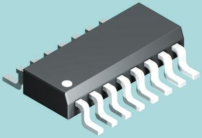
ICGOO电子元器件商城为您提供ISO7241MDW由Texas Instruments设计生产,在icgoo商城现货销售,并且可以通过原厂、代理商等渠道进行代购。 ISO7241MDW价格参考。Texas InstrumentsISO7241MDW封装/规格:数字隔离器, 通用 数字隔离器 2500Vrms 4 通道 150Mbps 25kV/µs CMTI 16-SOIC(0.295",7.50mm 宽)。您可以下载ISO7241MDW参考资料、Datasheet数据手册功能说明书,资料中有ISO7241MDW 详细功能的应用电路图电压和使用方法及教程。
Texas Instruments(德州仪器)的ISO7241MDW是一款数字隔离器,广泛应用于需要电气隔离以确保安全和信号完整性的各种场景。以下是该型号的主要应用场景:

 1. 工业自动化与控制系统
在工业环境中,设备之间的通信往往需要电气隔离来防止地线噪声、电磁干扰(EMI)以及高压瞬变对系统的影响。ISO7241MDW可以用于PLC(可编程逻辑控制器)、DCS(分布式控制系统)等设备中,确保数据传输的可靠性和安全性,同时保护敏感电路免受高电压冲击。

 2. 电机驱动与逆变器
电机驱动和逆变器系统通常工作在高电压和大电流环境下,容易产生电磁干扰和共模噪声。通过使用ISO7241MDW进行信号隔离,可以有效减少这些干扰对控制信号的影响,确保系统的稳定运行。此外,它还可以保护操作人员和设备免受电击风险。

 3. 医疗设备
在医疗设备中,患者的安全是首要考虑因素。ISO7241MDW可以用于心电图机、监护仪、超声设备等医疗器械中,提供必要的电气隔离,防止漏电流对患者的伤害。同时,它还能确保设备内部不同模块之间的信号传输不会受到干扰,保证测量结果的准确性。

 4. 电力系统与能源管理
电力系统中的智能电表、电力监控设备等需要在高电压环境下工作,ISO7241MDW可以用于隔离低压控制电路与高压主电路,确保数据采集和通信的可靠性。此外,在太阳能逆变器、风力发电系统等新能源领域,该器件也能起到关键作用,保护系统免受瞬态电压的影响。

 5. 通信与网络设备
在网络交换机、路由器等通信设备中,ISO7241MDW可以用于隔离不同端口之间的信号,防止信号串扰和噪声干扰。特别是在长距离通信或复杂电磁环境下,这种隔离有助于提高系统的抗干扰能力和稳定性。

总之,ISO7241MDW凭借其高性能的电气隔离特性,适用于多种对安全性和信号完整性要求较高的应用场景,能够有效提升系统的可靠性和稳定性。
| 参数 | 数值 |
| 产品目录 | |
| ChannelType | 单向 |
| 描述 | DGTL ISO 2.5KV GEN PURP 16SOIC数字隔离器 Quad Ch 3/1 150Mbps Dig Iso |
| 产品分类 | |
| IsolatedPower | 无 |
| 品牌 | Texas Instruments |
| 产品手册 | |
| 产品图片 |
|
| rohs | 符合RoHS无铅 / 符合限制有害物质指令(RoHS)规范要求 |
| 产品系列 | 接口 IC,数字隔离器,Texas Instruments ISO7241MDW- |
| 数据手册 | |
| 产品型号 | ISO7241MDW |
| PCN设计/规格 | |
| PulseWidthDistortion(Max) | 2ns |
| 上升/下降时间(典型值) | 2ns, 2ns |
| 产品目录页面 | |
| 产品种类 | |
| 传播延迟tpLH/tpHL(最大值) | 23ns, 23ns |
| 传播延迟时间 | 19 ns |
| 供应商器件封装 | 16-SOIC |
| 共模瞬态抗扰度(最小值) | 25kV/µs |
| 其它名称 | 296-22964-5 |
| 制造商产品页 | http://www.ti.com/general/docs/suppproductinfo.tsp?distId=10&orderablePartNumber=ISO7241MDW |
| 包装 | 管件 |
| 单位重量 | 420.400 mg |
| 反向通道 | 1 Channel |
| 商标 | Texas Instruments |
| 安装风格 | SMD/SMT |
| 封装 | Tube |
| 封装/外壳 | 16-SOIC(0.295",7.50mm 宽) |
| 封装/箱体 | SOIC-16 Wide |
| 工作温度 | -40°C ~ 125°C |
| 工厂包装数量 | 40 |
| 技术 | 容性耦合 |
| 数据速率 | 150Mbps |
| 最大工作温度 | + 125 C |
| 最大数据速率 | 150 Mb/s |
| 最小工作温度 | - 40 C |
| 标准包装 | 40 |
| 正向通道 | 3 Channel |
| 电压-电源 | 3.15 V ~ 5.5 V |
| 电压-隔离 | 2500Vrms |
| 电源电压-最大 | 5 V |
| 电源电压-最小 | 3.3 V |
| 类型 | General Purpose |
| 系列 | ISO7241M |
| 绝缘电压 | 4 kVrms |
| 脉宽失真(最大) | 2ns |
| 输入-输入侧1/输入侧2 | 3/1 |
| 通道数 | 4 |
| 通道数量 | 4 Channel |
| 通道类型 | 单向 |
| 配用 | /product-detail/zh/ISO723X724XEVM/296-30949-ND/1898682 |
| 隔离式电源 | 无 |

.jpg)


- 商务部:美国ITC正式对集成电路等产品启动337调查
- 曝三星4nm工艺存在良率问题 高通将骁龙8 Gen1或转产台积电
- 太阳诱电将投资9.5亿元在常州建新厂生产MLCC 预计2023年完工
- 英特尔发布欧洲新工厂建设计划 深化IDM 2.0 战略
- 台积电先进制程称霸业界 有大客户加持明年业绩稳了
- 达到5530亿美元!SIA预计今年全球半导体销售额将创下新高
- 英特尔拟将自动驾驶子公司Mobileye上市 估值或超500亿美元
- 三星加码芯片和SET,合并消费电子和移动部门,撤换高东真等 CEO
- 三星电子宣布重大人事变动 还合并消费电子和移动部门
- 海关总署:前11个月进口集成电路产品价值2.52万亿元 增长14.8%


PDF Datasheet 数据手册内容提取
Product Order Technical Tools & Support & Folder Now Documents Software Community ISO7240CF,ISO7240C,ISO7240M ISO7241C,ISO7241M,ISO7242C,ISO7242M SLLS868T–SEPTEMBER2007–REVISEDAPRIL2017 ISO724x High-Speed, Quad-Channel Digital Isolators 1 Features 3 Description • 25and150-MbpsSignalingRateOptions The ISO7240x, ISO7241x, and ISO7242x devices are 1 quad-channel digital isolators with multiple channel – LowChannel-to-ChannelOutputSkew; configurations and output-enable functions. These 1nsMaximum devices have logic-input and logic-output buffers – LowPulse-WidthDistortion(PWD); separated by Texas Instrument’s silicon-dioxide 2nsMaximum (SiO2) isolation barrier. Used in conjunction with isolated power supplies, these devices help block – LowJitterContent;1nsTypat150Mbps high voltage, isolate grounds, and prevent noise • SelectableDefaultOutput(ISO7240CF) currentsfromenteringthelocalgroundandinterfering • >25-YearLifeatRatedWorkingVoltage withordamagingsensitivecircuitry. (seeHigh-VoltageLifetimeoftheISO72xFamily The ISO7240x family of devices has all four channels ofDigitalIsolators andIsolationCapacitorLifetime in the same direction. The ISO7241x family of Projection) devices has three channels in the same direction and • 4-kVESDProtection one channel in the opposition direction. The ISO7242x family of devices has two channels in each • OperatesWith3.3-Vor5-VSupplies direction. • HighElectromagneticImmunity (seeISO72xDigitalIsolatorMagnetic-Field DeviceInformation(1) Immunity) PARTNUMBER PACKAGE BODYSIZE(NOM) • –40°Cto+125°COperatingTemperatureRange ISO7240CF • Safety-RelatedCertifications: ISO7240C – VDE4000V BasicInsulationperDINVVDE ISO7240M PK V0884-10(VDEV0884-10):2006-12 ISO7241C SOIC(16) 10.30mm×7.50mm – 2.5kV Insulationfor1minuteperUL1577 ISO7241M RMS – CSAComponentAcceptanceNotice#5Aand ISO7242C IEC60950-1EndEquipmentStandard ISO7242M (1) For all available packages, see the orderable addendum at 2 Applications theendofthedatasheet. • IndustrialFieldbus • ComputerPeripheralInterface • ServoControlInterface • DataAcquisition SimplifiedSchematic VCCI VCCO Isolation Capacitor INx OUTx Disable ENx (ISO7240CF only) or CTRL (ISO7240CF only) GNDI GNDO Copyright © 2016, Texas Instruments Incorporated V andGNDIaresupplyandgroundconnectionsrespectivelyfortheinputchannels. CCI V andGNDOaresupplyandgroundconnectionsrespectivelyfortheoutputchannels. CCO 1 An IMPORTANT NOTICE at the end of this data sheet addresses availability, warranty, changes, use in safety-critical applications, intellectualpropertymattersandotherimportantdisclaimers.PRODUCTIONDATA.
ISO7240CF,ISO7240C,ISO7240M ISO7241C,ISO7241M,ISO7242C,ISO7242M SLLS868T–SEPTEMBER2007–REVISEDAPRIL2017 www.ti.com Table of Contents 1 Features.................................................................. 1 7.18 SwitchingCharacteristics:VCC1at5-V,VCC2at3.3- VOperation.............................................................16 2 Applications........................................................... 1 7.19 SwitchingCharacteristics:V at3.3-VandV 3 Description............................................................. 1 CC1 CC2 at5-VOperation.......................................................17 4 RevisionHistory..................................................... 2 7.20 SwitchingCharacteristics:V andV at3.3-V CC1 CC2 5 Description(Continued)........................................ 7 Operation ................................................................17 6 PinConfigurationsandFunctions....................... 8 7.21 InsulationCharacteristicsCurves.........................18 7 Specifications......................................................... 9 7.22 TypicalCharacteristics..........................................19 7.1 AbsoluteMaximumRatings......................................9 8 ParameterMeasurementInformation................21 7.2 ESDRatings..............................................................9 9 DetailedDescription............................................ 24 7.3 RecommendedOperatingConditions.......................9 9.1 Overview.................................................................24 7.4 ThermalInformation................................................10 9.2 FunctionalBlockDiagram.......................................24 7.5 PowerRatings.........................................................10 9.3 FeatureDescription.................................................25 7.6 InsulationSpecifications..........................................11 9.4 DeviceFunctionalModes........................................25 7.7 Safety-RelatedCertifications...................................11 10 ApplicationandImplementation........................ 27 7.8 SafetyLimitingValues............................................12 10.1 ApplicationInformation..........................................27 7.9 ElectricalCharacteristics:VCC1andVCC2at5-V 10.2 TypicalApplication................................................27 Operation.................................................................12 11 PowerSupplyRecommendations..................... 32 7.10 SupplyCurrentCharacteristics:V andV at5- CC1 CC2 12 Layout................................................................... 32 VOperation..............................................................12 12.1 LayoutGuidelines.................................................32 7.11 ElectricalCharacteristics:V at5-V,V at3.3-V CC1 CC2 Operation.................................................................13 12.2 LayoutExample....................................................32 7.12 SupplyCurrentCharacteristics:V at5-V,V at 13 DeviceandDocumentationSupport................. 33 CC1 CC2 3.3-VOperation........................................................13 13.1 DocumentationSupport........................................33 7.13 ElectricalCharacteristics:VCC1at3.3-V,VCC2at5-V 13.2 RelatedLinks........................................................33 Operation.................................................................14 13.3 ReceivingNotificationofDocumentationUpdates33 7.14 SupplyCurrentCharacteristics:V at3.3-V,V CC1 CC2 13.4 CommunityResources..........................................33 at5-VOperation.......................................................14 13.5 Trademarks...........................................................33 7.15 ElectricalCharacteristics:V andV at3.3V CC1 CC2 13.6 ElectrostaticDischargeCaution............................34 Operation.................................................................15 13.7 Glossary................................................................34 7.16 SupplyCurrentCharacteristics:V andV at CC1 CC2 3.3VOperation........................................................15 14 Mechanical,Packaging,andOrderable 7.17 SwitchingCharacteristics:V andV at5-V Information........................................................... 34 CC1 CC2 Operation.................................................................16 4 Revision History NOTE:Pagenumbersforpreviousrevisionsmaydifferfrompagenumbersinthecurrentversion. ChangesfromRevisionS(April2016)toRevisionT Page • Addedisolationresistancefor100°C≤T ≤125°CintheInsulationSpecificationstable................................................... 11 A • DeletedthemaximumtransientovervoltagefromVDEintheSafety-RelatedCertificationstable...................................... 11 • AddedtheReceivingNotificationofDocumentationUpdatesandtheCommunityResourcessection............................... 33 ChangesfromRevisionR(September2015)toRevisionS Page • ChangedtheHBMvaluefrom±4Vto±4000VandtheCDMvaluefrom±1Vto±1000VintheESDRatingstable.........9 • MovedthedevicepowerdissipationparameterfromtheThermalInformationtabletothePowerDissipation Characteristicstable ............................................................................................................................................................ 10 ChangesfromRevisionQ(January2015)toRevisionR Page • ChangedFeaturesFrom:"BasicIsolationperDINEN60747-5-5(VDE0884-5)&DINEN61010-1"To:"Basic InsulationperDINVVDEV0884-10(VDEV0884-10):2006-12"......................................................................................... 1 • ChangedV ToV ,V ToV ,GND1ToGNDI,andGND2ToGNDO,andaddedNotes1and2tothe CC1 CCI CC2 CCO 2 SubmitDocumentationFeedback Copyright©2007–2017,TexasInstrumentsIncorporated ProductFolderLinks:ISO7240CF ISO7240C ISO7240MISO7241C ISO7241M ISO7242C ISO7242M
ISO7240CF,ISO7240C,ISO7240M ISO7241C,ISO7241M,ISO7242C,ISO7242M www.ti.com SLLS868T–SEPTEMBER2007–REVISEDAPRIL2017 SimplifiedSchematic.............................................................................................................................................................. 1 • ChangedtheCTITestConditionsFrom:IEC60112/VDE0303Part1To:DINEN60112(VDE0303-11);IEC60112 inthePackageCharacteristicstable ................................................................................................................................... 11 • ChangedsectiontitleFrom:DINEN60747-5-5InsulationCharacteristicsTo:DINVVDEV0884-10(VDEV0884- 10):2006-1InsulationCharacteristics(.................................................................................................................................. 11 • DeletedC -InputcapacitancetogroundfromthePackageCharacteristicstable ............................................................. 11 I • ChangedR TestConditionsFrom:V =500VatT To:V =500VatT =150°CintheDINVVDEV0884-10 S IO S IO S (VDEV0884-10):2006-1InsulationCharacteristicstable.................................................................................................... 11 • Changed"DINEN60747-5-5&DINEN61010-1"To:DINVVDEV0884-10(VDEV0884-10):2006-12andDINEN 61010-1(VDE0411-1):2011-07intheRegulatoryInformationtable.................................................................................. 11 • ChangedtitleFrom:IECSafetyLimitingValuesTo:SafetyLimitingValues....................................................................... 12 • ChangedV MINvaluesFrom:V -0.8To:V -0.8andV -0.1To:V -0.1intheElectrical OH CC CCO CC CCO Characteristics:V andV at5-VOperation ................................................................................................................. 12 CC1 CC2 • ChangedV TestConditionISO7240To:3.3-VsideandtheMINvalueFrom:V -0.4ToV -0.4inthe OH CC CCO ElectricalCharacteristics:V at5-V,V at3.3-VOperation.......................................................................................... 13 CC1 CC2 • ChangedV TestConditionISO724x(5-Vside)To:5-VsideandtheMINvalueFrom:V -0.8To:V -0.8in OH CC CCO theElectricalCharacteristics:V at5-V,V at3.3-VOperation.................................................................................... 13 CC1 CC2 • ChangedV ,TestConditionI =-20µAMINvalueFrom:V -0.1ToV -0.1inthelectricalCharacteristics: OH OH CC CCO VCC1at5-V,VCC2at3.3-VOperation............................................................................................................................... 13 • ChangedV TestConditionISO7240To:3.3-VsideandtheMINvalueFrom:V -0.4ToV -0.4inthe OH CC CCO ElectricalCharacteristics:V at3.3-V,V at5-VOperation.......................................................................................... 14 CC1 CC2 • ChangedV TestConditionISO724x(5-Vside)To:5-VsideandtheMINvalueFrom:V -0.8To:V -0.8in OH CC CCO theElectricalCharacteristics:V at3.3-V,V at5-VOperation.................................................................................... 14 CC1 CC2 • ChangedV ,TestConditionI =-20µAMINvalueFrom:V -0.1ToV -0.1intheElectricalCharacteristics: OH OH CC CCO V at3.3-V,V at5-VOperation.................................................................................................................................... 14 CC1 CC2 • ChangedV MINvaluesFrom:V -0.4To:V -0.4andV -0.1To:V -0.1intheElectrical OH CC CCO CC CCO Characteristics:V andV at3.3VOperation .............................................................................................................. 15 CC1 CC2 • ChangedFigure2titleFrom:ThermalDeratingCurveperDINEN60747-5-5To:ThermalDeratingCurveperVDE......18 • ChangedV To:V andV To:V inCommon-ModeTransientImmunityTestCircuitandVoltageWaveform ...23 CC1 CCI CC2 CCO ChangesfromRevisionP(August2014)toRevisionQ Page • ChangedtheV MAXvalueintheAbsoluteMaximumRatingstableFrom:6VTo:V +0.5V..........................................9 I CC • AddedNote3totheAbsoluteMaximumRatingstable.......................................................................................................... 9 • MovedT -StorageFromtheESDRatingstabletotheAbsoluteMaximumRatingstable.............................................. 9 STG • ChangedtheHandlingRatingtabletotheESDRatingstable. ............................................................................................. 9 • AddedonerowtotheISO7240CFFunctionsTabletable.Values:X,PD,X,X,X,Undetermined .................................... 25 • AddedonerowtotheDeviceFunctionTableISO724xtable.Values:X,PD,X,X,Undetermined ................................... 25 • ChangedtheDeviceI/OSchematicslabelsFrom:"ISO7240CFInput"To:"ISO7240CFInput,Disable"andFrom: "Enable"To:"Enable,Control" ............................................................................................................................................ 26 ChangesfromRevisionO(November2012)toRevisionP Page • AddedPinConfigurationandFunctionssection,HandlingRatingtable,FeatureDescriptionsection,Device FunctionalModes,ApplicationandImplementationsection,PowerSupplyRecommendationssection,Layout section,DeviceandDocumentationSupportsection,andMechanical,Packaging,andOrderableInformation section ................................................................................................................................................................................... 1 • ChangedISO7241Cminimumsupplyfrom2.8Vto3.15V................................................................................................... 9 Copyright©2007–2017,TexasInstrumentsIncorporated SubmitDocumentationFeedback 3 ProductFolderLinks:ISO7240CF ISO7240C ISO7240MISO7241C ISO7241M ISO7242C ISO7242M
ISO7240CF,ISO7240C,ISO7240M ISO7241C,ISO7241M,ISO7242C,ISO7242M SLLS868T–SEPTEMBER2007–REVISEDAPRIL2017 www.ti.com ChangesfromRevisionN(January2012)toRevisionO Page • AddedtheSafetyLimitingValuessection............................................................................................................................ 12 ChangesfromRevisionM(January2011)toRevisionN Page • ChangedFeatureFrom:Operates3.3-Vor5-VSuppliesTo:OperatesWith2.8-V(ISO7241C),3.3-Vor5-VSupplies..... 1 • AddeddeviceoptionstoV intheRECOMMENDEDOPERATINGCONDITIONStable................................................... 9 CC • ChangedTableNote(1)......................................................................................................................................................... 9 • ChangedtheCTIMINvalueFrom:≥175VTo:≥400V........................................................................................................ 11 • ChangedtheRegulatoryInformationtable........................................................................................................................... 11 • ChangedTableNote(1)....................................................................................................................................................... 12 • ChangedI andI testconditionsintheV andV at5-VElectricalCharacteristics:V andV at5-V CC1 CC2 CC1 CC2 CC1 CC2 Operationtable..................................................................................................................................................................... 12 • ChangedTableNote(1)....................................................................................................................................................... 13 • ChangedI andI testconditionsintheV at5-V,V at3.3-VElectricalCharacteristics:V at5-V,V at CC1 CC2 CC1 CC2 CC1 CC2 3.3-VOperationtable........................................................................................................................................................... 13 • ChangedTableNote(1)....................................................................................................................................................... 14 • ChangedI andI testconditionsintheV at3.3-V,V at5-VElectricalCharacteristics:V at3.3-V,V CC1 CC2 CC1 CC2 CC1 CC2 at5-VOperationtable.......................................................................................................................................................... 14 • ChangedTableNote(1)....................................................................................................................................................... 15 • AddedELECTRICALandSwitchingCHARACTERISTICStablesforV andV at2.8V(ISO722xC-only)...................15 CC1 CC2 • ChangedI andI testconditionsintheV andV at3.3Vtable.......................................................................... 15 CC1 CC2 CC1 CC2 • ChangedV UndervoltageThresholdvsFree-AirTemperatureFromV FailsafeThresholdTo:V Undervoltage CC CC1 CC Threshold.............................................................................................................................................................................. 19 ChangesfromRevisionL(January2010)toRevisionM Page • ChangedtheCSAFileNumberFrom:1698195To:220991............................................................................................... 11 • ChangedSwitchingCharacteristicTestCircuitandVoltageWaveforms,FailsafeDelayTimeTestCircuitand VoltageWaveforms,andWakeTimeFromInputDisableTestCircuitandVoltageWaveforms........................................ 21 ChangesfromRevisionK(Decemberl2009)toRevisionL Page • AddedCTI-Trackingresistance(comparativetrackingindextothePackageCharacteristicstable.................................. 11 • AddedtheIEC60664-1RATINGSTABLE.......................................................................................................................... 11 • AddedtheIEC60747-5-2INSULATIONCHARACTERISTICtable..................................................................................... 11 ChangesfromRevisionJ(April2009)toRevisionK Page • ChangedtheInputcircuitintheDEVICEI/OSCHEMATICSillustration............................................................................... 1 • AddedNote1toLI01),andchangedtheMINvalueFrom:8.34To8mminthePackageCharacteristicstable ..............11 • AddedNote1toLI02),andchangedtheMINvalueFrom:8.1To8mminthePackageCharacteristicstable ................11 ChangesfromRevisionI(December2008)toRevisionJ Page • ChangedI forQuiescentand1MbpsFrom:10mATo:11mA......................................................................................... 12 CC1 • ChangedI forQuiescentand1MbpsFrom:10mATo:11mA......................................................................................... 13 CC1 4 SubmitDocumentationFeedback Copyright©2007–2017,TexasInstrumentsIncorporated ProductFolderLinks:ISO7240CF ISO7240C ISO7240MISO7241C ISO7241M ISO7242C ISO7242M
ISO7240CF,ISO7240C,ISO7240M ISO7241C,ISO7241M,ISO7242C,ISO7242M www.ti.com SLLS868T–SEPTEMBER2007–REVISEDAPRIL2017 ChangesfromRevisionG(July2008)toRevisionH Page • AddedDevicenumberISO7240CF........................................................................................................................................ 1 • AddedFeaturesBullet:SelectableFailsafeOutput(ISO7240CF)......................................................................................... 1 • Changeddescriptionparagraph4text................................................................................................................................... 7 • ChangedV intheAbsoluteMaximumRatingstableFrom:VoltageatIN,OUT,ENTo:VoltageatIN,OUT,EN, I DISABLE,CTRL..................................................................................................................................................................... 9 • Addedt ,Waketimefrominputdisable........................................................................................................................... 16 wake • Addedt ,Waketimefrominputdisable........................................................................................................................... 16 wake • Addedt ,Waketimefrominputdisable........................................................................................................................... 17 wake • Addedt ,Waketimefrominputdisable........................................................................................................................... 17 wake ChangesfromRevisionF(May2008)toRevisionG Page • ChangedthePackageCharacteristicstable,line,L MINvaluefrom7.7mmto8.34mm................................................ 11 (IO1) ChangesfromRevisionE(May2008)toRevisionF Page • DeletedISO724xAdevices.SeeSLLS905fortheISO7240A,ISO7241A,andISO7242A................................................... 1 • ChangedTitleFrom:QUADDIGITALISOLATORSTo:HIGHSPEEDQUADDIGITALISOLATORS................................. 1 • ChangedFeatureLowJitterContent-From:1,25,and150-MbpsSignalingRateOptionsTo:25,and150-Mbps SignalingRateOptions........................................................................................................................................................... 1 • Addedt footnote............................................................................................................................................................. 16 sk(pp) • Addedt footnote.............................................................................................................................................................. 16 sk(o) • Addedt footnote............................................................................................................................................................. 17 sk(pp) • Addedt footnote.............................................................................................................................................................. 17 sk(o) ChangesfromRevisionD(April2008)toRevisionE Page • AddedTableNote(1):Forthe5-Voperation,V orV isspecifiedfrom4.5Vto5.5V................................................ 9 CC1 CC2 • AddedTableNote(1):Forthe5-Voperation,V orV isspecifiedfrom4.5Vto5.5V.............................................. 13 CC1 CC2 • AddedTableNote(1):Forthe5-Voperation,V orV isspecifiedfrom4.5Vto5.5V.............................................. 14 CC1 CC2 • AddedTableNote(1):Forthe5-Voperation,V orV isspecifiedfrom4.5Vto5.5V.............................................. 15 CC1 CC2 ChangesfromRevisionC(April2008)toRevisionD Page • Addedt Part-to-partskew.............................................................................................................................................. 16 sk(pp) • Addedt Part-to-partskew.............................................................................................................................................. 16 sk(pp) • Addedt Part-to-partskew.............................................................................................................................................. 17 sk(pp) • Addedt Part-to-partskew.............................................................................................................................................. 17 sk(pp) • ChangedTypicalISO724xApplicationCircuit,IsolatedDataAcquisitionSystemforProcessControl .............................. 27 ChangesfromRevisionB(August2008)toRevisionC Page • DeletedMin=4.5Vandmax=5.5VforSupplyVoltageoftheROCTable........................................................................ 9 • ChangedV SupplyVoltageintheROCTableFrom:3.6To:5.5....................................................................................... 9 CC Copyright©2007–2017,TexasInstrumentsIncorporated SubmitDocumentationFeedback 5 ProductFolderLinks:ISO7240CF ISO7240C ISO7240MISO7241C ISO7241M ISO7242C ISO7242M
ISO7240CF,ISO7240C,ISO7240M ISO7241C,ISO7241M,ISO7242C,ISO7242M SLLS868T–SEPTEMBER2007–REVISEDAPRIL2017 www.ti.com ChangesfromRevisionA(December2007)toRevisionB Page • ChangedV SupplyVoltageintheROCTableFrom:3.45To:3.6..................................................................................... 9 CC ChangesfromOriginal(September2007)toRevisionA Page • ChangedV SupplyVoltageintheROCTableFrom:3.6To:3.45..................................................................................... 9 CC • ChangedV SupplyVoltageintheROCTableFrom:3To:3.15........................................................................................ 9 CC • ChangedC -typvalueFrom:1To:2................................................................................................................................ 11 IO • ChangedtheRegulatoryInformation.................................................................................................................................... 11 • ChangedC -typvalueFrom:1To:2intheElectricalCharacteristics:V andV at5-VOperation........................... 12 I CC1 CC2 • ChangedTBDstoactualvalues........................................................................................................................................... 12 • ChangedC -typvalueFrom:1To:2intheElectricalCharacteristics:V at5-V,V at3.3-VOperation....................13 I CC1 CC2 • ChangedC -typvalueFrom:1To:2intheElectricalCharacteristics:V at3.3-V,V at5-VOperation....................14 I CC1 CC2 • ChangedtypvalueFrom:1To:2intheElectricalCharacteristics:V andV at3.3VOperation............................... 15 CC1 CC2 • ChangedPropagationdelaymaxFrom:22To:23.............................................................................................................. 16 • ChangedPropagationdelaymaxFrom:46To:50.............................................................................................................. 16 • ChangedPropagationdelaymaxFrom:28To:29.............................................................................................................. 16 • ChangedISO724xA/CmaxvalueFrom:2.5To:3............................................................................................................... 16 • ChangedPropagationdelaymaxFrom:26To:30.............................................................................................................. 17 • ChangedPropagationdelaymaxFrom:32To:34.............................................................................................................. 17 • ChangedISO724xA/CmaxvalueFrom:3To:3.5............................................................................................................... 17 • ChangedISO7240C/MRMSSupplyCurrentvsSignalingRate,ISO7241C/MRMSSupplyCurrentvsSignaling Rate,andPropagationDelayvsFree-AirTemperature.AddedISO7242C/MRMSSupplyCurrentvsSignalingRate.....19 6 SubmitDocumentationFeedback Copyright©2007–2017,TexasInstrumentsIncorporated ProductFolderLinks:ISO7240CF ISO7240C ISO7240MISO7241C ISO7241M ISO7242C ISO7242M
ISO7240CF,ISO7240C,ISO7240M ISO7241C,ISO7241M,ISO7242C,ISO7242M www.ti.com SLLS868T–SEPTEMBER2007–REVISEDAPRIL2017 5 Description (Continued) The devices with the C suffix (C option) have TTL input thresholds and a noise-filter at the input that prevents transient pulses from being passed to the output of the device. The devices with the M suffix (M option) have CMOSV /2inputthresholdsanddonothavetheinputnoisefilterortheadditionalpropagationdelay. CC The ISO7240CF device has an input disable function on pin 7, and a selectable high or low failsafe-output function with the CTRL pin (pin 10). The failsafe output is a logic high when a logic high is placed on the CTRL pin or it is left unconnected. If a logic low signal is applied to the CTRL pin, the failsafe output becomes a logic- low output state. The input disable function of the ISO7240CF device prevents data from being passed across the isolation barrier to the output. When the inputs are disabled or V is powered down, the outputs are set by CC1 theCTRLpin. These devices can be powered from 3.3-V or 5-V supplies on either side, in any combination. The signal input pinsare5-Vtolerantregardlessofthevoltagesupplylevelthatisused. Thesedevicesarecharacterizedforoperationovertheambienttemperaturerangeof –40°Cto+125°C. Copyright©2007–2017,TexasInstrumentsIncorporated SubmitDocumentationFeedback 7 ProductFolderLinks:ISO7240CF ISO7240C ISO7240MISO7241C ISO7241M ISO7242C ISO7242M
ISO7240CF,ISO7240C,ISO7240M ISO7241C,ISO7241M,ISO7242C,ISO7242M SLLS868T–SEPTEMBER2007–REVISEDAPRIL2017 www.ti.com 6 Pin Configurations and Functions ISO7240CFDWPackage ISO7240CandISO7240MDWPackage 16-PinSOIC 16-PinSOIC TopView TopView VCC1 1 16 VCC2 VCC1 1 16 VCC2 GND1 2 15 GND2 GND1 2 15 GND2 INA 3 N 14 OUTA INA 3 N 14 OUTA O O INB 4 TI 13 OUTB INB 4 TI 13 OUTB A A INC 5 OL 12 OUTC INC 5 OL 12 OUTC IND 6 IS 11 OUTD IND 6 IS 11 OUTD DISABLE 7 10 CTRL NC 7 10 EN GND1 8 9 GND2 GND1 8 9 GND2 ISO7241CandISO7241MDWPackage ISO7242CandISO7242MDWPackage 16-PinSOIC 16-PinSOIC TopView TopView VCC1 1 16 VCC2 VCC1 1 16 VCC2 GND1 2 15 GND2 GND1 2 15 GND2 INA 3 N 14 OUTA INA 3 N 14 OUTA O O INB 4 TI 13 OUTB INB 4 TI 13 OUTB A A INC 5 OL 12 OUTC OUTC 5 OL 12 INC OUTD 6 IS 11 IND OUTD 6 IS 11 IND EN1 7 10 EN2 EN1 7 10 EN2 GND1 8 9 GND2 GND1 8 9 GND2 PinFunctions PIN NO. I/O DESCRIPTION3 NAME ISO7240C ISO7241C ISO7242C ISO7240CF ISO7240M ISO7241M ISO7242M CTRL 10 — — — I Failsafeoutputcontrol.OutputstateisdeterminedbyCTRLpinwhenDISABLEishighorVCC1is powereddown.OutputishighwhenCTRLishighoropenandlowwhenCTRLislow. Inputdisable.AllinputpinsaredisabledwhenDISABLEishighandenabledwhenDISABLEislowor DISABLE 7 — — — I open. EN — 10 — — I Outputenable.AlloutputpinsareenabledwhenENishighoropenanddisabledwhenENislow. EN1 — — 7 7 I Olouwt.putenable1.Outputpinsonside1areenabledwhenEN1ishighoropenanddisabledwhenEN1is EN2 — — 10 10 I Olouwt.putenable2.Outputpinsonside-2areenabledwhenEN2ishighoropenanddisabledwhenEN2is GND1 2,8 2,8 2,8 2,8 — GroundconnectionforVCC1 GND2 9,15 9,15 9,15 9,15 — GroundconnectionforVCC2 INA 3 3 3 3 I Input,channelA INB 4 4 4 4 I Input,channelB INC 5 5 5 12 I Input,channelC IND 6 6 11 11 I Input,channelD NC — 7 — — — NoConnectpinsarefloatingwithnointernalconnection OUTA 14 14 14 14 O Output,channelA OUTB 13 13 13 13 O Output,channelB OUTC 12 12 12 5 O Output,channelC OUTD 11 11 6 6 O Output,channelD VCC1 1 1 1 1 — Powersupply,VCC1 VCC2 16 16 16 16 — Powersupply,VCC2 8 SubmitDocumentationFeedback Copyright©2007–2017,TexasInstrumentsIncorporated ProductFolderLinks:ISO7240CF ISO7240C ISO7240MISO7241C ISO7241M ISO7242C ISO7242M
ISO7240CF,ISO7240C,ISO7240M ISO7241C,ISO7241M,ISO7242C,ISO7242M www.ti.com SLLS868T–SEPTEMBER2007–REVISEDAPRIL2017 7 Specifications 7.1 Absolute Maximum Ratings See (1) MIN MAX UNIT VCC Supplyvoltage(2),VCC1,VCC2 –0.5 6 V VI VoltageatIN,OUT,EN,DISABLE,CTRL –0.5 VCC+0.5(3) V IO Outputcurrent –15 15 mA TJ Maximumjunctiontemperature 170 °C Tstg Storagetemperature –65 150 °C (1) StressesbeyondthoselistedunderAbsoluteMaximumRatingsmaycausepermanentdamagetothedevice.Thesearestressratings onlyandfunctionaloperationofthedeviceattheseoranyotherconditionsbeyondthoseindicatedunderRecommendedOperating Conditionsisnotimplied.Exposuretoabsolute-maximum-ratedconditionsforextendedperiodsmayaffectdevicereliability. (2) Allvoltagevaluesarewithrespecttonetworkgroundterminalandarepeakvoltagevalues. (3) Maximumvoltagemustnotexceed6V. 7.2 ESD Ratings VALUE UNIT Humanbodymodel(HBM),perANSI/ESDA/JEDECJS-001(1) ±4000 V Electrostatic Chargeddevicemodel(CDM),perJEDECspecificationJESD22-C101(2) ±1000 V (ESD) discharge Machinemodel(MM),perANSI/ESDS5.2-1996 ±200 (1) JEDECdocumentJEP155statesthat500-VHBMallowssafemanufacturingwithastandardESDcontrolprocess. (2) JEDECdocumentJEP157statesthat250-VCDMallowssafemanufacturingwithastandardESDcontrolprocess. 7.3 Recommended Operating Conditions MIN NOM MAX UNIT VCC Supplyvoltage(1),VCC1,VCC2 3.15 5.5 V IOH High-leveloutputcurrent –4 mA IOL Low-leveloutputcurrent 4 mA ISO724xC 40 tui Inputpulsewidth ns ISO724xM 6.67 5 ISO724xC 0 30(2) 25 1/tui Signalingrate ISO724xM 0 200(2) 150 Mbps VIH High-levelinputvoltage(IN) 0.7VCC VCC V ISO724xM VIL Low-levelinputvoltage(IN) 0 0.3VCC V VIH High-levelinputvoltage(IN,DISABLE,CTRL,EN) 2 5.5 V ISO724xC VIL Low-levelinputvoltage(IN,DISABLE,CTRL,EN) 0 0.8 V TJ Junctiontemperature 150 °C H Externalmagneticfield-strengthimmunityperIEC61000-4-8andIEC61000-4-9certification 1000 A/m (1) Forthe5-Voperation,V orV isspecifiedfrom4.5Vto5.5V. CC1 CC2 Forthe3.3-Voperation,V orV isspecifiedfrom3.15Vto3.6V. CC1 CC2 (2) Typicalvalueatroomtemperatureandwell-regulatedpowersupply. Copyright©2007–2017,TexasInstrumentsIncorporated SubmitDocumentationFeedback 9 ProductFolderLinks:ISO7240CF ISO7240C ISO7240MISO7241C ISO7241M ISO7242C ISO7242M
ISO7240CF,ISO7240C,ISO7240M ISO7241C,ISO7241M,ISO7242C,ISO7242M SLLS868T–SEPTEMBER2007–REVISEDAPRIL2017 www.ti.com 7.4 Thermal Information ISO724xx THERMALMETRIC(1) DW(SOIC) UNIT 16PINS RθJA Junction-to-ambientthermal Low-Kboard 168 °C/W resistance High-Kboard 77.3 °C/W R Junction-to-case(top)thermalresistance 39.5 °C/W θJC(top) R Junction-to-boardthermalresistance 41.9 °C/W θJB ψ Junction-to-topcharacterizationparameter 13.5 °C/W JT ψ Junction-to-boardcharacterizationparameter 41.9 °C/W JB R Junction-to-case(bottom)thermalresistance n/a °C/W θJC(bot) (1) Formoreinformationabouttraditionalandnewthermalmetrics,seetheSemiconductorandICPackageThermalMetricsapplication report. 7.5 Power Ratings V =V =5.5V,T =150°C,C =15pF,Inputa50%dutycyclesquarewave(unlessotherwisenoted) CC1 CC2 J L PARAMETER TESTCONDITIONS MIN TYP MAX UNIT P Maximumpowerdissipation 220 mW D 10 SubmitDocumentationFeedback Copyright©2007–2017,TexasInstrumentsIncorporated ProductFolderLinks:ISO7240CF ISO7240C ISO7240MISO7241C ISO7241M ISO7242C ISO7242M
ISO7240CF,ISO7240C,ISO7240M ISO7241C,ISO7241M,ISO7242C,ISO7242M www.ti.com SLLS868T–SEPTEMBER2007–REVISEDAPRIL2017 7.6 Insulation Specifications PARAMETER TESTCONDITIONS VALUE UNIT GENERAL CLR Externalclearance(1) Shortestterminal-to-terminaldistancethroughair 8 mm CPG Externalcreepage(1) Shortestterminal-to-terminaldistanceacrossthe 8 mm packagesurface DTI Distancethroughtheinsulation Minimuminternalgap(internalclearance) 0.008 mm CTI Comparativetrackingindex DINEN60112(VDE0303-11);IEC60112 ≥400 V Materialgroup II Ratedmainsvoltage≤150V I-IV RMS OvervoltageCategory Ratedmainsvoltage≤300V I-III RMS DINVVDEV0884-10(VDEV0884-10):2006-12(2) V Maximumrepetitivepeakisolationvoltage ACvoltage(bipolar) 560 V IORM PK V =V V Maximumtransientisolationvoltage TEST IOTM 4000 V IOTM t=60s(qualification),t=1s(100%production) PK Methoda:AfterI/Osafetytestsubgroup2/3. V =VIOTM,t =60s; ≤5 ini ini V =1.2×V ,t =10s, pd(m) IORM m Methoda:Afterenvironmentaltestssubgroup1, q Apparentcharge(3) Vini=VIOTM,tini=60s; ≤5 pC pd V =1.3×V ,t =10s, pd(m) IORM m Methodb1:Atroutinetest(100%production)and preconditioning(typetest) ≤5 V =VIOTM,t =1s; ini ini V =1.5×V ,t =1s, pd(m) IORM m C Barriercapacitance,inputtooutput(4) V =0.4sin(4E6πt) 2 pF IO I V =500V,T =25°C >1012 IO A R Isolationresistance,inputtooutput(4) V =500V,100°C≤T ≤125°C >1011 Ω IO IO A V =500VatT =150°C >109 IO S Pollutiondegree 2 Climaticcategory 40/125/21 UL1577 V =V =2500V ,t=60s(qualification); TEST ISO RMS V Withstandisolationvoltage V =1.2×V =3000V ,t=1s(100% 2500 V ISO TEST ISO RMS RMS production) (1) Creepageandclearancerequirementsshouldbeappliedaccordingtothespecificequipmentisolationstandardsofanapplication.Care shouldbetakentomaintainthecreepageandclearancedistanceofaboarddesigntoensurethatthemountingpadsoftheisolatoron theprinted-circuitboarddonotreducethisdistance.Creepageandclearanceonaprinted-circuitboardbecomeequalincertaincases. Techniquessuchasinsertinggroovesand/orribsonaprintedcircuitboardareusedtohelpincreasethesespecifications. (2) Thiscouplerissuitableforbasicelectricalinsulationonlywithinthemaximumoperatingratings.Compliancewiththesafetyratingsshall beensuredbymeansofsuitableprotectivecircuits. (3) Apparentchargeiselectricaldischargecausedbyapartialdischarge(pd). (4) Allpinsoneachsideofthebarriertiedtogethercreatingatwo-terminaldevice 7.7 Safety-Related Certifications VDE CSA UL CertifiedaccordingtoDINVVDEV0884-10 ApprovedunderCSAComponent RecognizedunderUL1577Component (VDEV0884-10):2006-12andDINEN AcceptanceNotice5AandIEC60950-1 RecognitionProgram 61010-1(VDE0411-1):2011-07 BasicInsulation 4000V maximumisolationrating; MaximumTransientIsolationVoltage,4000 PK BasicinsulationperCSA60950-1-07and V ; Singleprotection,2500V PK IEC60950-1(2ndEd),366V maximum RMS MaximumRepetitivePeakIsolationVoltage, RMS workingvoltage, 560V PK CertificateNumber:40016131 MasterContractNumber:220991 FileNumber:E181974 Copyright©2007–2017,TexasInstrumentsIncorporated SubmitDocumentationFeedback 11 ProductFolderLinks:ISO7240CF ISO7240C ISO7240MISO7241C ISO7241M ISO7242C ISO7242M
ISO7240CF,ISO7240C,ISO7240M ISO7241C,ISO7241M,ISO7242C,ISO7242M SLLS868T–SEPTEMBER2007–REVISEDAPRIL2017 www.ti.com 7.8 Safety Limiting Values Safetylimiting(1)intendstominimizepotentialdamagetotheisolationbarrieruponfailureofinputoroutputcircuitry.Afailure oftheI/Ocanallowlowresistancetogroundorthesupplyand,withoutcurrentlimiting,dissipatesufficientpowertooverheat thedieanddamagetheisolationbarrier,potentiallyleadingtosecondarysystemfailures. PARAMETER TESTCONDITIONS MIN TYP MAX UNIT R =168°C/W,V =5.5V,T =170°C,T =25°C, θJA I J A 156 Safetyinput,output,orsupply seeFigure2 I mA S current R =168°C/W,V =3.6V,T =170°C,T =25°C, θJA I J A 239 seeFigure2 T Safetytemperature 150 °C S (1) Thesafety-limitingconstraintisthemaximumjunctiontemperaturespecifiedinthedatasheet.Thepowerdissipationandjunction-to-air thermalimpedanceofthedeviceinstalledintheapplicationhardwaredeterminesthejunctiontemperature.Theassumedjunction-to-air thermalresistanceintheThermalInformationtableisthatofadeviceinstalledonahigh-Ktestboardforleadedsurface-mount packages.Thepoweristherecommendedmaximuminputvoltagetimesthecurrent.Thejunctiontemperatureisthentheambient temperatureplusthepowertimesthejunction-to-airthermalresistance. 7.9 Electrical Characteristics: V and V at 5-V Operation CC1 CC2 Forthe5-Voperation,V orV isspecifiedfrom4.5Vto5.5V.Overrecommendedoperatingconditions(unless CC1 CC2 otherwisenoted) PARAMETER TESTCONDITIONS MIN TYP MAX UNIT IOFF Sleepmodeoutputcurrent ENat0V,Singlechannel 0 μA IOH=–4mA,SeeFigure11 VCCO–0.8 VOH High-leveloutputvoltage V IOH=–20μA,SeeFigure11 VCCO–0.1 IOL=4mA,SeeFigure11 0.4 VOL Low-leveloutputvoltage V IOL=20μA,SeeFigure11 0.1 VI(HYS) Inputvoltagehysteresis 150 mV IIH High-levelinputcurrent INatVCCI 10 μA IIL Low-levelinputcurrent INat0V –10 CI Inputcapacitancetoground INatVCC,VI=0.4sin(4E6πt) 2 pF CMTI Common-modetransientimmunity VI=VCCor0V,SeeFigure15 25 50 kV/μs 7.10 Supply Current Characteristics: V and V at 5-V Operation CC1 CC2 Forthe5-Voperation,V orV isspecifiedfrom4.5Vto5.5V.Overrecommendedoperatingconditions(unless CC1 CC2 otherwisenoted) PARAMETER TESTCONDITIONS MIN TYP MAX UNIT ISO7240C/M Quiescent,Allchannels,noload,ENat3V,VI=VCCor0V 1 3 ICC1 Supplycurrent,side1 mA 25Mbps,Allchannels,noload,ENat3V,12.5-MHzinput-clocksignal 7 10.5 Quiescent,VI=VCCor0V 15 22 ICC2 Supplycurrent,side2 Allchannels,noload,ENat3V mA 25Mbps,12.5-MHzinput-clocksignal 17 25 ISO7241C/M Quiescent,VI=VCCor0V 6.5 11 ICC1 Supplycurrent,side1 Allchannels,noload,EN1at3V,EN2at3V mA 25Mbps,12.5-MHzinput-clocksignal 12 18 Quiescent,VI=VCCor0V 13 20 ICC2 Supplycurrent,side2 Allchannels,noload,EN1at3V,EN2at3V mA 25Mbps,12.5-MHzinput-clocksignal 18 28 ISO7242C/M Quiescent,VI=VCCor0V 10 16 ICC1 Supplycurrent,side1 Allchannels,noload,EN1at3V,EN2at3V mA 25Mbps,12.5-MHzinput-clocksignal 15 24 Allchannels,noload, Quiescent,VI=VCCor0V 10 16 ICC2 Supplycurrent,side2 EN1at3V,EN2at3V 25Mbps,12.5-MHzinput-clocksignal 15 24 mA 12 SubmitDocumentationFeedback Copyright©2007–2017,TexasInstrumentsIncorporated ProductFolderLinks:ISO7240CF ISO7240C ISO7240MISO7241C ISO7241M ISO7242C ISO7242M
ISO7240CF,ISO7240C,ISO7240M ISO7241C,ISO7241M,ISO7242C,ISO7242M www.ti.com SLLS868T–SEPTEMBER2007–REVISEDAPRIL2017 7.11 Electrical Characteristics: V at 5-V, V at 3.3-V Operation CC1 CC2 Forthe5-Voperation,V orV isspecifiedfrom4.5Vto5.5V.Forthe3.3-Voperation,V orV isspecifiedfrom CC1 CC2 CC1 CC2 3.15Vto3.6V.Overrecommendedoperatingconditions(unlessotherwisenoted) PARAMETER TESTCONDITIONS MIN TYP MAX UNIT IOFF Sleepmodeoutputcurrent ENat0V,Singlechannel 0 μA 3.3-Vside VCCO–0.4 IOH=–4mA,SeeFigure11 VOH High-leveloutputvoltage 5-Vside VCCO–0.8 V IOH=–20μA,SeeFigure11 VCCO–0.1 IOL=4mA,SeeFigure11 0.4 VOL Low-leveloutputvoltage V IOL=20μA,SeeFigure11 0.1 VI(HYS) Inputvoltagehysteresis 150 mV IIH High-levelinputcurrent INatVCCI 10 μA IIL Low-levelinputcurrent INat0V –10 CI Inputcapacitancetoground INatVCC,VI=0.4sin(4E6πt) 2 pF CMTI Common-modetransientimmunity VI=VCCor0V,SeeFigure15 25 50 kV/μs 7.12 Supply Current Characteristics: V at 5-V, V at 3.3-V Operation CC1 CC2 Forthe5-Voperation,V orV isspecifiedfrom4.5Vto5.5V.Forthe3.3-Voperation,V orV isspecifiedfrom CC1 CC2 CC1 CC2 3.15Vto3.6V.Overrecommendedoperatingconditions(unlessotherwisenoted) PARAMETER TESTCONDITIONS MIN TYP MAX UNIT ISO7240C/M Quiescent,VI=VCCor0V 1 3 ICC1 Supplycurrent,side1 Allchannels,noload,ENat3V mA 25Mbps,12.5-MHzinput-clocksignal 7 10.5 Quiescent,VI=VCCor0V 9.5 15 ICC2 Supplycurrent,side2 Allchannels,noload,ENat3V mA 25Mbps,12.5-MHzinput-clocksignal 10.5 17 ISO7241C/M Quiescent,VI=VCCor0V 6.5 11 ICC1 Supplycurrent,side1 Allchannels,noload,EN1at3V,EN2at3V mA 12.5-MHzinput-clocksignal 12 18 Quiescent,VI=VCCor0V 8 13 ICC2 Supplycurrent,side2 Allchannels,noload,EN1at3V,EN2at3V mA 25Mbps,12.5-MHzinput-clocksignal 11.5 18 ISO7242C/M Quiescent,VI=VCCor0V 10 16 ICC1 Supplycurrent,side1 Allchannels,noload,EN1at3V,EN2at3V mA 12.5-MHzinput-clocksignal 15 24 Quiescent,VI=VCCor0V 6 10 ICC2 Supplycurrent,side2 Allchannels,noload,EN1at3V,EN2at3V mA 25Mbps,12.5-MHzinput-clocksignal 9 14 Copyright©2007–2017,TexasInstrumentsIncorporated SubmitDocumentationFeedback 13 ProductFolderLinks:ISO7240CF ISO7240C ISO7240MISO7241C ISO7241M ISO7242C ISO7242M
ISO7240CF,ISO7240C,ISO7240M ISO7241C,ISO7241M,ISO7242C,ISO7242M SLLS868T–SEPTEMBER2007–REVISEDAPRIL2017 www.ti.com 7.13 Electrical Characteristics: V at 3.3-V, V at 5-V Operation CC1 CC2 Forthe5-Voperation,V orV isspecifiedfrom4.5Vto5.5V.Forthe3.3-Voperation,V orV isspecifiedfrom CC1 CC2 CC1 CC2 3.15Vto3.6V.Overrecommendedoperatingconditions(unlessotherwisenoted) PARAMETER TESTCONDITIONS MIN TYP MAX UNIT IOFF Sleepmodeoutputcurrent ENat0V,Singlechannel 0 μA 3.3-Vside VCCO–0.4 IOH=–4mA,SeeFigure11 VOH High-leveloutputvoltage 5-Vside VCCO–0.8 V IOH=–20μA,SeeFigure11 VCCO–0.1 IOL=4mA,SeeFigure11 0.4 VOL Low-leveloutputvoltage V IOL=20μA,SeeFigure11 0.1 VI(HYS) Inputvoltagehysteresis 150 mV IIH High-levelinputcurrent INatVCCI 10 μA IIL Low-levelinputcurrent INat0V –10 CI Inputcapacitancetoground INatVCC,VI=0.4sin(4E6πt) 2 pF CMTI Common-modetransientimmunity VI=VCCor0V,SeeFigure15 25 50 kV/μs 7.14 Supply Current Characteristics: V at 3.3-V, V at 5-V Operation CC1 CC2 Forthe5-Voperation,V orV isspecifiedfrom4.5Vto5.5V.Forthe3.3-Voperation,V orV isspecifiedfrom CC1 CC2 CC1 CC2 3.15Vto3.6V.Overrecommendedoperatingconditions(unlessotherwisenoted) PARAMETER TESTCONDITIONS MIN TYP MAX UNIT ISO7240C/M Quiescent,VI=VCCor0V 0.5 1 ICC1 Supplycurrent,side1 Allchannels,noload,ENat3V mA 25Mbps,12.5-MHzinput-clocksignal 3 5 Quiescent,VI=VCCor0V 15 22 ICC2 Supplycurrent,side2 Allchannels,noload,ENat3V mA 25Mbps,12.5-MHzinput-clocksignal 17 25 ISO7241C/M Quiescent,VI=VCCor0V 4 7 ICC1 Supplycurrent,side1 Allchannels,noload,EN1at3V,EN2at3V mA 25Mbps,12.5-MHzinput-clocksignal 6.5 11 Quiescent,VI=VCCor0V 13 20 ICC2 Supplycurrent,side2 Allchannels,noload,EN1at3V,EN2at3V mA 25Mbps,12.5-MHzinput-clocksignal 18 28 ISO7242C/M Quiescent,VI=VCCor0V 6 10 ICC1 Supplycurrent,side1 Allchannels,noload,EN1at3V,EN2at3V mA 25Mbps,12.5-MHzinput-clocksignal 9 14 Quiescent,VI=VCCor0V 10 16 ICC2 Supplycurrent,side2 Allchannels,noload,EN1at3V,EN2at3V mA 25Mbps,12.5-MHzinput-clocksignal 15 24 14 SubmitDocumentationFeedback Copyright©2007–2017,TexasInstrumentsIncorporated ProductFolderLinks:ISO7240CF ISO7240C ISO7240MISO7241C ISO7241M ISO7242C ISO7242M
ISO7240CF,ISO7240C,ISO7240M ISO7241C,ISO7241M,ISO7242C,ISO7242M www.ti.com SLLS868T–SEPTEMBER2007–REVISEDAPRIL2017 7.15 Electrical Characteristics: V and V at 3.3 V Operation CC1 CC2 Forthe3.3-Voperation,V orV isspecifiedfrom3.15Vto3.6V.Overrecommendedoperatingconditions(unless CC1 CC2 otherwisenoted) PARAMETER TESTCONDITIONS MIN TYP MAX UNIT IOFF Sleepmodeoutputcurrent ENat0V,singlechannel 0 μA IOH=–4mA,SeeFigure11 VCCO–0.4 VOH High-leveloutputvoltage V IOH=–20μA,SeeFigure11 VCCO–0.1 IOL=4mA,SeeFigure11 0.4 VOL Low-leveloutputvoltage V IOL=20μA,SeeFigure11 0.1 VI(HYS) Inputvoltagehysteresis 150 mV IIH High-levelinputcurrent INatVCCI 10 μA IIL Low-levelinputcurrent INat0V –10 CI Inputcapacitancetoground INatVCC,VI=0.4sin(4E6πt) 2 pF CMTI Common-modetransientimmunity VI=VCCor0V,SeeFigure15 25 50 kV/μs 7.16 Supply Current Characteristics: V and V at 3.3 V Operation CC1 CC2 Forthe3.3-Voperation,V orV isspecifiedfrom3.15Vto3.6V.Overrecommendedoperatingconditions(unless CC1 CC2 otherwisenoted) PARAMETER TESTCONDITIONS MIN TYP MAX UNIT ISO7240C/M Quiescent,VI=VCCor0V 0.5 1 ICC1 Supplycurrent,side1 Allchannels,noload,ENat3V mA 25Mbps,12.5-MHzinput-clocksignal 3 5 Quiescent,VI=VCCor0V 9.5 15 ICC2 Supplycurrent,side2 Allchannels,noload,ENat3V mA 25Mbps,12.5-MHzinput-clocksignal 10.5 17 ISO7241C/M Quiescent,VI=VCCor0V 4 7 ICC1 Supplycurrent,side1 Allchannels,noload,EN1at3V,EN2at3V mA 25Mbps,12.5-MHzinput-clocksignal 6.5 11 Quiescent,VI=VCCor0V 8 13 ICC2 Supplycurrent,side2 Allchannels,noload,EN1at3V,EN2at3V mA 25Mbps,12.5-MHzinput-clocksignal 11.5 18 ISO7242C/M Quiescent,VI=VCCor0V 6 10 ICC1 Supplycurrent,side1 Allchannels,noload,EN1at3V,EN2at3V mA 25Mbps,12.5-MHzinput-clocksignal 9 14 Quiescent,VI=VCCor0V 6 10 ICC2 Supplycurrent,side2 Allchannels,noload,EN1at3V,EN2at3V mA 25Mbps,12.5-MHzinput-clocksignal 9 14 Copyright©2007–2017,TexasInstrumentsIncorporated SubmitDocumentationFeedback 15 ProductFolderLinks:ISO7240CF ISO7240C ISO7240MISO7241C ISO7241M ISO7242C ISO7242M
ISO7240CF,ISO7240C,ISO7240M ISO7241C,ISO7241M,ISO7242C,ISO7242M SLLS868T–SEPTEMBER2007–REVISEDAPRIL2017 www.ti.com 7.17 Switching Characteristics: V and V at 5-V Operation CC1 CC2 overrecommendedoperatingconditions(unlessotherwisenoted) PARAMETER TESTCONDITIONS MIN TYP MAX UNIT tPLH, Propagationdelay 18 42 tPHL ISO724xC ns PWD Pulse-widthdistortion(1)|tPHL–tPLH| 2.5 SeeFigure11 tPLH, Propagationdelay 10 23 tPHL ISO724xM ns PWD Pulse-widthdistortion(1)|tPHL–tPLH| 1 2 ISO724xC 8 tsk(pp) Part-to-partskew(2) ns ISO724xM 0 3 ISO724xC 2 tsk(o) Channel-to-channeloutputskew(3) ns ISO724xM 0 1 tr Outputsignalrisetime 2 SeeFigure11 ns tf Outputsignalfalltime 2 tPHZ Propagationdelay,high-level-to-high-impedanceoutput 15 20 tPZH Propagationdelay,high-impedance-to-high-leveloutput 15 20 SeeFigure12 ns tPLZ Propagationdelay,low-level-to-high-impedanceoutput 15 20 tPZL Propagationdelay,high-impedance-to-low-leveloutput 15 20 tfs Failsafeoutputdelaytimefrominputpowerloss SeeFigure13 12 μs twake Waketimefrominputdisable SeeFigure14 15 μs 150MbpsNRZdatainput,Samepolarity tjit(pp) Peak-to-peakeye-patternjitter ISO724xM inputonallchannels,SeeFigure16 1 ns (1) Alsoreferredtoaspulseskew. (2) t isthemagnitudeofthedifferenceinpropagationdelaytimesbetweenanyspecifiedterminalsoftwodeviceswhenbothdevices sk(pp) operatewiththesamesupplyvoltages,atthesametemperature,andhaveidenticalpackagesandtestcircuits. (3) t istheskewbetweenspecifiedoutputsofasingledevicewithalldrivinginputsconnectedtogetherandtheoutputsswitchinginthe sk(o) samedirectionwhiledrivingidenticalspecifiedloads. 7.18 Switching Characteristics: V at 5-V, V at 3.3-V Operation CC1 CC2 overrecommendedoperatingconditions(unlessotherwisenoted) PARAMETER TESTCONDITIONS MIN TYP MAX UNIT tPLH,tPHL Propagationdelay 20 50 ISO724xC ns PWD Pulse-widthdistortion(1)|tPHL–tPLH| 3 SeeFigure11 tPLH,tPHL Propagationdelay 12 29 ISO724xM ns PWD Pulse-widthdistortion(1)|tPHL–tPLH| 1 2 ISO724xC 10 tsk(pp) Part-to-partskew(2) ns ISO724xM 0 5 ISO724xC 3 tsk(o) Channel-to-channeloutputskew(3) ns ISO724xM 0 1 tr Outputsignalrisetime 2 SeeFigure11 ns tf Outputsignalfalltime 2 tPHZ Propagationdelay,high-level-to-high-impedanceoutput 15 20 tPZH Propagationdelay,high-impedance-to-high-leveloutput 15 20 SeeFigure12 ns tPLZ Propagationdelay,low-level-to-high-impedanceoutput 15 20 tPZL Propagationdelay,high-impedance-to-low-leveloutput 15 20 tfs Failsafeoutputdelaytimefrominputpowerloss SeeFigure13 18 μs twake Waketimefrominputdisable SeeFigure14 15 μs 150MbpsPRBSNRZdatainput,Same tjit(pp) Peak-to-peakeye-patternjitter ISO724xM polarityinputonallchannels,SeeFigure16 1 ns (1) Alsoknownaspulseskew (2) t isthemagnitudeofthedifferenceinpropagationdelaytimesbetweenanyspecifiedterminalsoftwodeviceswhenbothdevices sk(pp) operatewiththesamesupplyvoltages,atthesametemperature,andhaveidenticalpackagesandtestcircuits. (3) t istheskewbetweenspecifiedoutputsofasingledevicewithalldrivinginputsconnectedtogetherandtheoutputsswitchinginthe sk(o) samedirectionwhiledrivingidenticalspecifiedloads. 16 SubmitDocumentationFeedback Copyright©2007–2017,TexasInstrumentsIncorporated ProductFolderLinks:ISO7240CF ISO7240C ISO7240MISO7241C ISO7241M ISO7242C ISO7242M
ISO7240CF,ISO7240C,ISO7240M ISO7241C,ISO7241M,ISO7242C,ISO7242M www.ti.com SLLS868T–SEPTEMBER2007–REVISEDAPRIL2017 7.19 Switching Characteristics: V at 3.3-V and V at 5-V Operation CC1 CC2 overrecommendedoperatingconditions(unlessotherwisenoted) PARAMETER TESTCONDITIONS MIN TYP MAX UNIT tPLH,tPHL Propagationdelay 22 51 ISO724xC ns PWD Pulse-widthdistortion(1)|tPHL–tPLH| 3 SeeFigure11 tPLH,tPHL Propagationdelay 12 30 ISO724xM ns PWD Pulse-widthdistortion(1)|tPHL–tPLH| 1 2 ISO724xC 10 tsk(pp) Part-to-partskew(2) ns ISO724xM 0 5 ISO724xC 2.5 tsk(o) Channel-to-channeloutputskew(3) ns ISO724xM 0 1 tr Outputsignalrisetime 2 SeeFigure11 ns tf Outputsignalfalltime 2 tPHZ Propagationdelay,high-level-to-high-impedanceoutput 15 20 tPZH Propagationdelay,high-impedance-to-high-leveloutput 15 20 SeeFigure12 ns tPLZ Propagationdelay,low-level-to-high-impedanceoutput 15 20 tPZL Propagationdelay,high-impedance-to-low-leveloutput 15 20 tfs Failsafeoutputdelaytimefrominputpowerloss SeeFigure13 12 μs twake Waketimefrominputdisable SeeFigure14 15 μs 150MbpsNRZdatainput,Samepolarity tjit(pp) Peak-to-peakeye-patternjitter ISO724xM inputonallchannels,SeeFigure16 1 ns (1) Alsoknownaspulseskew (2) t isthemagnitudeofthedifferenceinpropagationdelaytimesbetweenanyspecifiedterminalsoftwodeviceswhenbothdevices sk(pp) operatewiththesamesupplyvoltages,atthesametemperature,andhaveidenticalpackagesandtestcircuits. (3) t istheskewbetweenspecifiedoutputsofasingledevicewithalldrivinginputsconnectedtogetherandtheoutputsswitchinginthe sk(o) samedirectionwhiledrivingidenticalspecifiedloads. 7.20 Switching Characteristics: V and V at 3.3-V Operation CC1 CC2 overrecommendedoperatingconditions(unlessotherwisenoted) PARAMETER TESTCONDITIONS MIN TYP MAX UNIT tPLH,tPHL Propagationdelay 25 56 ISO724xC ns PWD Pulse-widthdistortion|tPHL–tPLH|(1) 4 SeeFigure11 tPLH,tPHL Propagationdelay 12 34 ISO724xM ns PWD Pulse-widthdistortion|tPHL–tPLH|(1) 1 2 ISO724xC 10 tsk(pp) Part-to-partskew(2) ns ISO724xM 0 5 ISO724xC 3.5 tsk(o) Channel-to-channeloutputskew(3) ns ISO724xM 0 1 tr Outputsignalrisetime 2 ns SeeFigure11 tf Outputsignalfalltime 2 ns tPHZ Propagationdelay,high-level-to-high-impedanceoutput 15 20 tPZH Propagationdelay,high-impedance-to-high-leveloutput 15 20 SeeFigure12 ns tPLZ Propagationdelay,low-level-to-high-impedanceoutput 15 20 tPZL Propagationdelay,high-impedance-to-low-leveloutput 15 20 tfs Failsafeoutputdelaytimefrominputpowerloss SeeFigure13 18 μs twake Waketimefrominputdisable SeeFigure14 15 μs 150MbpsPRBSNRZdatainput,same tjit(pp) Peak-to-peakeye-patternjitter ISO724xM polarityinputonallchannels,SeeFigure16 1 ns (1) Alsoreferredtoaspulseskew. (2) t isthemagnitudeofthedifferenceinpropagationdelaytimesbetweenanyspecifiedterminalsoftwodeviceswhenbothdevices sk(pp) operatewiththesamesupplyvoltages,atthesametemperature,andhaveidenticalpackagesandtestcircuits. (3) t istheskewbetweenspecifiedoutputsofasingledevicewithalldrivinginputsconnectedtogetherandtheoutputsswitchinginthe sk(o) samedirectionwhiledrivingidenticalspecifiedloads. Copyright©2007–2017,TexasInstrumentsIncorporated SubmitDocumentationFeedback 17 ProductFolderLinks:ISO7240CF ISO7240C ISO7240MISO7241C ISO7241M ISO7242C ISO7242M
ISO7240CF,ISO7240C,ISO7240M ISO7241C,ISO7241M,ISO7242C,ISO7242M SLLS868T–SEPTEMBER2007–REVISEDAPRIL2017 www.ti.com 7.21 Insulation Characteristics Curves 100 300 VCC1,2at 3.6 V s] 250 ear mA Working Life [Y 28Years VIORMat 560 VPK miting Current - 125000 VCC1,2at 5.5 V Li y 100 et 10 Saf 0 120 250 500 750 880 1000 50 Working Voltage (V ) [V ] IORM PK 0 0 50 100 150 200 TC- Case Temperature - °C Figure1.IsolationCapacitorLifetimeProjection Figure2.ThermalDeratingCurveforLimitingCurrentper VDE 18 SubmitDocumentationFeedback Copyright©2007–2017,TexasInstrumentsIncorporated ProductFolderLinks:ISO7240CF ISO7240C ISO7240MISO7241C ISO7241M ISO7242C ISO7242M
ISO7240CF,ISO7240C,ISO7240M ISO7241C,ISO7241M,ISO7242C,ISO7242M www.ti.com SLLS868T–SEPTEMBER2007–REVISEDAPRIL2017 7.22 Typical Characteristics 45 45 40 40 I- Supply Current - mA/RMSCC 121233055005 5-V ICC2 3.3-V ICC2 5-V ICC1 I- Supply Current - mA/RMSCC 112233050505 5-V ICC2 33.5.33--V-VV I ICICCCCC121 5 3.3-V I 5 CC1 0 0 0 25 50 75 100 125 150 0 25 50 75 100 125 150 Signaling Rate - Mbps Signaling Rate - Mbps TA=25°C Load=15pF AllChannels TA=25°C Load=15pF AllChannels Figure3.ISO7240C/MRMSSupplyCurrentvs Figure4.ISO7241C/MRMSSupplyCurrentvs SignalingRate SignalingRate 45 45 40 40 3.3-VtpLH,tpHL(C-grade) MS 35 35 y Current - mA/R 223050 5-V ICC1,ICC2 ation Delay - ns 223050 3.3-VtpLH, tpHL(M-grade) 5-VtpLH, tpHL(C-grade) - SupplC 15 3.3-V ICC1,ICC2 Propag 15 5-VtpLH, tpHL(M-grade) IC 10 10 5 5 0 0 0 25 50 75 100 125 150 -40 -25 -10 5 20 35 50 65 80 95 110 125 Signaling Rate - Mbps TA- Free-Air Temperature -°C TA=25°C Load=15pF AllChannels TA=25°C Load=15pF AllChannels Figure5.ISO7242C/MRMSSupplyCurrentvs Figure6.PropagationDelayvsFree-AirTemperature SignalingRate 1.4 3 5 V V 1.35 th+ 2.9 V - 2.8 Input Voltage Threshold - V 11..11112...55123 5 V Vth- 3.3 V Vth+ V-Undervoltage ThresholdCC 222222......234567 VVCCCCRFiaslilningg 1.05 2.1 3.3 V V th- 1 2 -40 -25 -10 5 20 35 50 65 80 95 110 125 -40 -25 -10 5 20 35 50 65 80 95 110 125 TA- Free-Air Temperature -°C TA- Free-Air Temperature -°C AirFlowat7cf/m Low_KBoard Figure7.InputVoltageThresholdvsFree-AirTemperature Figure8.VCCUndervoltageThresholdvs Free-AirTemperature Copyright©2007–2017,TexasInstrumentsIncorporated SubmitDocumentationFeedback 19 ProductFolderLinks:ISO7240CF ISO7240C ISO7240MISO7241C ISO7241M ISO7242C ISO7242M
ISO7240CF,ISO7240C,ISO7240M ISO7241C,ISO7241M,ISO7242C,ISO7242M SLLS868T–SEPTEMBER2007–REVISEDAPRIL2017 www.ti.com Typical Characteristics (continued) 50 50 V = 5 V CC 45 40 40 mA VCC= 3.3 V mA 35 Current - 30 Current - 2350 VCC= 3.3 V V = 5 V ut ut CC utp 20 utp 20 O O - O - O 15 I I 10 10 5 0 0 2 4 6 00 1 2 3 4 5 VO- Output Voltage - V VO- Output Voltage - V TA=25°C Load=15pF TA=25°C Load=15pF Figure9.High-LevelOutputCurrentvs Figure10.Low-LevelOutputCurrentvs High-LevelOutputVoltage Low-LevelOutputVoltage 20 SubmitDocumentationFeedback Copyright©2007–2017,TexasInstrumentsIncorporated ProductFolderLinks:ISO7240CF ISO7240C ISO7240MISO7241C ISO7241M ISO7242C ISO7242M
ISO7240CF,ISO7240C,ISO7240M ISO7241C,ISO7241M,ISO7242C,ISO7242M www.ti.com SLLS868T–SEPTEMBER2007–REVISEDAPRIL2017 8 Parameter Measurement Information er VCC IN Barri OUT VI VCC/2 VCC/2 n 0 V o Input olati tPLH tPHL (SGeeen Neroateto Ar ) VI 50 (cid:13) Is VO CSeLe Note B VOH 90% VO 50% 50% 10% VOL tr tf Copyright © 2016, Texas Instruments Incorporated A. Theinputpulseissuppliedbyageneratorhavingthefollowingcharacteristics:PRR≤50kHz,50%dutycycle,t ≤3 r ns,t ≤3ns,Z =50Ω. f O B. C =15pFandincludesinstrumentationandfixturecapacitancewithin±20%. L Figure11. SwitchingCharacteristicTestCircuitandVoltageWaveforms VCC VCC arrier RL = 1 k(cid:13)(cid:3)±1% VI VCC/2 VCC/2 IN B OUT 0 V on VO tPZL tPLZ 0 V olati VCC Is EN 0.5 V VO 50% See NoteC BL VOL Input Generator (See Note A) VI 50 (cid:13) IN Barrier OUT VO VCC 3 V olation VI VCC / 2 VCC / 2 0 V Is EN tPZH CL RL = 1 k(cid:13)(cid:3)±1% VOH Input See Note B VO 50% 0.5 V (SGeeen Neroateto Ar ) VI 50 (cid:13) tPHZ 0 V Copyright © 2016, Texas Instruments Incorporated A. Theinputpulseissuppliedbyageneratorhavingthefollowingcharacteristics:PRR≤50kHz,50%dutycycle,t ≤3 r ns,t ≤3ns,Z =50Ω. f O B. C =15pFandincludesinstrumentationandfixturecapacitancewithin±20%. L Figure12. EnableorDisablePropagation-DelayTimeTestCircuitandWaveform Copyright©2007–2017,TexasInstrumentsIncorporated SubmitDocumentationFeedback 21 ProductFolderLinks:ISO7240CF ISO7240C ISO7240MISO7241C ISO7241M ISO7242C ISO7242M
ISO7240CF,ISO7240C,ISO7240M ISO7241C,ISO7241M,ISO7242C,ISO7242M SLLS868T–SEPTEMBER2007–REVISEDAPRIL2017 www.ti.com Parameter Measurement Information (continued) VI VCC VCC er VI 2.7 V 0 V (fs high) arri 0 V VCC1 (fs lowo)r IN ation B OUT VO tfs fs high VOH Isol CL VO 50% fs low See Note A VOL A. C =15pFandincludesinstrumentationandfixturecapacitancewithin±20%. L Figure13. FailsafeDelayTimeTestCircuitandVoltageWaveforms er VCC 3 V IN n Barri OUT VO VI VCC/2 o olati 0 V s CRTL DISABLE I 0 V CL twake VCC See Note B Input (SGeeen Neroateto Ar ) VI 50 (cid:13) VO 50% 0 V IN Barrier OUT VO VCC 0 V on VI VCC/2 ati ol DISABLE Is CRTL 0 V 3 V CL twake See Note B VCC Input Generator 50 (cid:13) (See Note A) VI 50% VO 0 V Copyright © 2016, Texas Instruments Incorporated NOTE: Thetestthatyieldsthelongesttimeisusedinthisdatasheet. A. Theinputpulseissuppliedbyageneratorhavingthefollowingcharacteristics:PRR≤50kHz,50%dutycycle,t ≤3 r ns,t ≤3ns,Z =50Ω. f O B. C =15pFandincludesinstrumentationandfixturecapacitancewithin±20%. L Figure14. WakeTimeFromInputDisableTestCircuitandVoltageWaveforms 22 SubmitDocumentationFeedback Copyright©2007–2017,TexasInstrumentsIncorporated ProductFolderLinks:ISO7240CF ISO7240C ISO7240MISO7241C ISO7241M ISO7242C ISO7242M
ISO7240CF,ISO7240C,ISO7240M ISO7241C,ISO7241M,ISO7242C,ISO7242M www.ti.com SLLS868T–SEPTEMBER2007–REVISEDAPRIL2017 Parameter Measurement Information (continued) V V CCI CCO C = 0.1 µF ±1% C = 0.1 µF ±1% Pass-fail criteria– output must remain er stable. arri IN B OUT S1 n atio + ol s C V or V I L OH OL See NoteA – GNDI GNDO + V – CM A. C =15pFandincludesinstrumentationandfixturecapacitancewithin±20%. L B. Theinputpulseissuppliedbyageneratorhavingthefollowingcharacteristics:PRR≤50kHz,50%dutycycle,t ≤3 r ns,t ≤3ns,Z =50Ω. f O Figure15. Common-ModeTransientImmunityTestCircuitandVoltageWaveform VCC DUT Input IN Tektronix 0 V HFS9009 Tektronix 784D Pattern OUT Generator Output VCC/2 Jitter Copyright © 2016, Texas Instruments Incorporated NOTE: PRBSbitpatternrunlengthis216–1.Transitiontimeis800ps.NRZdatainputhasnomorethanfiveconsecutive1s or0s. Figure16. Peak-to-PeakEye-PatternJitterTestCircuitandVoltageWaveform Copyright©2007–2017,TexasInstrumentsIncorporated SubmitDocumentationFeedback 23 ProductFolderLinks:ISO7240CF ISO7240C ISO7240MISO7241C ISO7241M ISO7242C ISO7242M
ISO7240CF,ISO7240C,ISO7240M ISO7241C,ISO7241M,ISO7242C,ISO7242M SLLS868T–SEPTEMBER2007–REVISEDAPRIL2017 www.ti.com 9 Detailed Description 9.1 Overview The isolator in Figure 17 is based on a capacitive isolation-barrier technique. The I/O channel of the device consists of two internal data channels, a high-frequency channel (HF) with a bandwidth from 100 kbps up to 150 Mbps, and a low-frequency channel (LF) covering the range from 100 kbps down to DC. In principle, a single- ended input signal entering the HF-channel is split into a differential signal through the inverter gate at the input. The following capacitor-resistor networks differentiate the signal into transients, which then are converted into differential pulses by two comparators. The comparator outputs drive a NOR-gate flip-flop the output of which feeds an output multiplexer. A decision logic (DCL) at the driving output of the flip-flop measures the durations between signal transients. If the duration between two consecutive transients exceeds a certain time limit, as in the case of a low-frequency signal, the DCL forces the output-multiplexer to switch from the high- to the low- frequencychannel. Because low-frequency input signals require the internal capacitors to assume prohibitively large values, these signals are pulse-width modulated (PWM) with the carrier frequency of an internal oscillator, thus creating a sufficientlyhighfrequencysignal,capableofpassingthecapacitivebarrier.Astheinputismodulated,alow-pass filter(LPF)isrequiredtoremovethehigh-frequencycarrierfromtheactualdatabeforepassingitontotheoutput multiplexer. 9.2 Functional Block Diagram Isolation Barrier OSC LPF Low t Frequency Channel PWM VREF (DC...100 kbps) 0 OUT 1 S IN DCL High t Frequency Channel VREF (100 kbps...150 Mbps) Copyright © 2016, Texas Instruments Incorporated Figure17. ConceptualBlockDiagramofaDigitalCapacitiveIsolator 24 SubmitDocumentationFeedback Copyright©2007–2017,TexasInstrumentsIncorporated ProductFolderLinks:ISO7240CF ISO7240C ISO7240MISO7241C ISO7241M ISO7242C ISO7242M
ISO7240CF,ISO7240C,ISO7240M ISO7241C,ISO7241M,ISO7242C,ISO7242M www.ti.com SLLS868T–SEPTEMBER2007–REVISEDAPRIL2017 9.3 Feature Description The ISO724xx family of devices is available in multiple channel configurations and default output-state options to enablewidevarietyofapplicationuses.Table1liststhesedevicefeatures. Table1.DeviceFeatures SIGNALING INPUT CHANNEL PRODUCT RATE THRESHOLD CONFIGURATION ISO7240C 25Mbps ~1.5V(TTL) ISO7240CF 25Mbps ~1.5V(TTL) 4/0 ISO7240M 150Mbps V /2(CMOS) CC ISO7241C 25Mbps ~1.5V(TTL) 3/1 ISO7241M 150Mbps V /2(CMOS) CC ISO7242C 25Mbps ~1.5V(TTL) 2/2 ISO7242M 150Mbps V /2(CMOS) CC 9.4 Device Functional Modes Table2liststheISO724xxfunctionalmodes.Table3 liststheISO7240CFfunctionalmodes. Table2.DeviceFunctionTableISO724x(1) INPUT OUTPUTENABLE OUTPUT INPUTV OUTPUTV CC CC (IN) (EN) (OUT) H HorOpen H L HorOpen L PU PU X L Z Open HorOpen H PD PU X HorOpen H PD PU X L Z X PD X X Undetermined (1) PU=PoweredUp;PD=PoweredDown;X=Irrelevant;H=HighLevel;L=LowLevel;Z=High Impedance;Open=NotConnected Table3.ISO7240CFFunctionsTable(1) DATAINPUT DISABLEINPUT FAILSAFECONTROL DATAOUTPUT V V CC1 CC2 (IN) (DISABLE) (CTRL) (OUT) PU PU H LorOpen X H PU PU L LorOpen X L X PU X H HorOpen H X PU X H L L PD PU X X HorOpen H PD PU X X L L X PD X X X Undetermined (1) PU=PoweredUp;PD=PoweredDown;X=Irrelevant;H=HighLevel;L=LowLevel;Z=HighImpedance;Open=NotConnected Copyright©2007–2017,TexasInstrumentsIncorporated SubmitDocumentationFeedback 25 ProductFolderLinks:ISO7240CF ISO7240C ISO7240MISO7241C ISO7241M ISO7242C ISO7242M
ISO7240CF,ISO7240C,ISO7240M ISO7241C,ISO7241M,ISO7242C,ISO7242M SLLS868T–SEPTEMBER2007–REVISEDAPRIL2017 www.ti.com 9.4.1 DeviceI/OSchematics Input Output V VCC VCC VCC CC 1 MW 500W 8W IN OUT 13W ISO7240CF Enable, Control Input, Disable VCC VCC VCC VCC VCC 1 MW IN 500W EN 500W or or DISABLE CTRL 1 MW Copyright © 2016,Texas Instruments Incorporated Figure18. DeviceI/OSchematics 26 SubmitDocumentationFeedback Copyright©2007–2017,TexasInstrumentsIncorporated ProductFolderLinks:ISO7240CF ISO7240C ISO7240MISO7241C ISO7241M ISO7242C ISO7242M
ISO7240CF,ISO7240C,ISO7240M ISO7241C,ISO7241M,ISO7242C,ISO7242M www.ti.com SLLS868T–SEPTEMBER2007–REVISEDAPRIL2017 10 Application and Implementation NOTE Information in the following applications sections is not part of the TI component specification, and TI does not warrant its accuracy or completeness. TI’s customers are responsible for determining suitability of components for their purposes. Customers should validateandtesttheirdesignimplementationtoconfirmsystemfunctionality. 10.1 Application Information The ISO724xx family of devices uses a single-ended TTL or CMOS-logic switching technology. The supply voltage range is from 3.15 V to 5.5 V for both supplies, V and V . When designing with digital isolators, CC1 CC2 keep in mind that because of the single-ended design structure, digital isolators do not conform to any specific interface standard and are only intended for isolating single-ended CMOS or TTL digital signal lines. The isolator is typically placed between the data controller (that is, μC or UART), and a data converter or a line transceiver, regardlessoftheinterfacetypeorstandard. 10.2 Typical Application 10.2.1 IsolatedDataAcquisitionSystemforProcessControl The ISO724xx family of devices can be used with Texas Instruments' precision analog-to-digital converter and mixedsignalmicrocontrollertocreateanadvancedisolateddataacquisitionsystemasshowninFigure19. Isolation 5 VISO 5 VISO Barrier 5 VISO 3.3 V 3.3 V 0.1 (cid:29)F 0.1 (cid:29)F 16 1 0.1 (cid:29)F AVD2D2 D1VDD 0.1 (cid:29)F 10 VCC2 VCC1 7 0.1 (cid:29)F 2 EN2 EN1 11 RTD AIN1+ A0 8 14 OUTA INA 3 11 P3.0 DVcc XOUT 5 12 AIN1– A1 7 13 OUTBISO7241 INB 4 12 P3.1 27 12 5 14 MSP430F2132 6 SCLK OUTC INC CLK XIN 18 28 11 6 13 18 Bridge AIN2+ DOUT IND OUTD SOMI P3.7 17 AIN2–ADS1234 5 VISO 5 VISO 9, 15 GND2 GND1 2, 8 3.3 V 15 P3.6 1176 20 P3.4 P3.5 Thermo 13 AIN3+ RREEFF+– 19 0.1 (cid:29)F0.1 (cid:29)F 1106 VCC2 VCC1 71 0.1 (cid:29)F D4Vss EN NC couple 14 AIN3– 23 14 3 GAIN0 OUTA INA 24 13 ISO7240 4 16 GAIN1 OUTB INB AIN4+ 25 12 5 Current SPEED OUTC INC shunt 15 26 11 6 AIN4– PWDN OUTD IND 9, 15 2, 8 AGND DGND GND2 GND1 21 2 Copyright © 2016, Texas Instruments Incorporated Figure19. IsolatedDataAcquisitionSystemforProcessControl 10.2.1.1 DesignRequirements Unlike optocouplers, which require external components to improve performance, provide bias, or limit current, theISO724xfamilyofdevicesonlyrequiretwoexternalbypasscapacitorstooperate. Copyright©2007–2017,TexasInstrumentsIncorporated SubmitDocumentationFeedback 27 ProductFolderLinks:ISO7240CF ISO7240C ISO7240MISO7241C ISO7241M ISO7242C ISO7242M
ISO7240CF,ISO7240C,ISO7240M ISO7241C,ISO7241M,ISO7242C,ISO7242M SLLS868T–SEPTEMBER2007–REVISEDAPRIL2017 www.ti.com Typical Application (continued) 10.2.1.2 DetailedDesignProcedure 2 mm maximum 2 mm maximum from VCC1 from VCC2 0.1 µF ISO7240C and ISO7240M 0.1 µF 1 16 VCC2 VCC1 GND1 2 15 GND2 INA 3 14 OUTA INB 4 13 OUTB INC 5 12 OUTC IND 6 11 OUTD NC EN 7 10 GND1 GND2 8 9 Copyright © 2016, Texas Instruments Incorporated Figure20. ISO7240xTypicalCircuitHook-Up 2 mm maximum 2 mm maximum from VCC1 from VCC2 0.1 µF ISO7240CF 0.1 µF 1 16 VCC2 VCC1 GND1 2 15 GND2 INA 3 14 OUTA INB 4 13 OUTB INC 5 12 OUTC IND 6 11 OUTD DISABLE CTRL 7 10 GND1 GND2 8 9 Copyright © 2016, Texas Instruments Incorporated Figure21. ISO7240CFTypicalCircuitHook-Up 28 SubmitDocumentationFeedback Copyright©2007–2017,TexasInstrumentsIncorporated ProductFolderLinks:ISO7240CF ISO7240C ISO7240MISO7241C ISO7241M ISO7242C ISO7242M
ISO7240CF,ISO7240C,ISO7240M ISO7241C,ISO7241M,ISO7242C,ISO7242M www.ti.com SLLS868T–SEPTEMBER2007–REVISEDAPRIL2017 Typical Application (continued) 2 mm maximum 2 mm maximum from VCC1 from VCC2 0.1 µF ISO7241C and ISO7241M 0.1 µF 1 16 VCC2 VCC1 GND1 2 15 GND2 INA 3 14 OUTA INB 4 13 OUTB INC 5 12 OUTC OUTD 6 11 IND EN1 EN2 7 10 GND1 GND2 8 9 Copyright © 2016, Texas Instruments Incorporated Figure22. ISO7241xTypicalCircuitHook-Up 2 mm maximum 2 mm maximum from VCC1 from VCC2 0.1 µF ISO7242C and ISO7242M 0.1 µF 1 16 VCC2 VCC1 GND1 2 15 GND2 INA 3 14 OUTA INB 4 13 OUTB OUTC 5 12 INC OUTD 6 11 IND EN1 EN2 7 10 GND1 GND2 8 9 Copyright © 2016, Texas Instruments Incorporated Figure23. ISO7242xTypicalCircuitHook-Up Copyright©2007–2017,TexasInstrumentsIncorporated SubmitDocumentationFeedback 29 ProductFolderLinks:ISO7240CF ISO7240C ISO7240MISO7241C ISO7241M ISO7242C ISO7242M
ISO7240CF,ISO7240C,ISO7240M ISO7241C,ISO7241M,ISO7242C,ISO7242M SLLS868T–SEPTEMBER2007–REVISEDAPRIL2017 www.ti.com Typical Application (continued) 10.2.1.3 ApplicationCurves Figure24.ISO7242MEyeDiagramat25Mbps, Figure25.ISO7242MEyeDiagramat150Mbps, 3.3Vand25°C 3.3Vand25°C 10.2.2 IsolatedSPIforanAnalogInputModulewith16Inputs TheISO7241xfamilyofdevicesandseveralothercomponentsfromTexasInstrumentscanbeusedtocreatean isolatedSPIforaninputmodulewith16inputs. VS 3.3 V 0.1 (cid:29)F VC2C D2 3 1:1.33 MBR0520L 4 IN OUT 1 3.3VISO TLV70733 SN6501 10 (cid:29)F 0.1 (cid:29)F 10 (cid:29)F 3 2 EN GND 1 GND D1 2 VIN VOUT 6 10 (cid:29)F MBR0520L 4, 5 1 (cid:29)F REF5025 22 (cid:29)F 4 Isolation Barrier GND 0.1 (cid:29)F 0.1 (cid:29)F 0.1 (cid:29)F 0.1 (cid:29)F 1 16 4.7 k(cid:13) 4.7 k(cid:13) VCC1 VCC2 2 7 10 3 2 28 32 31 DVCC 6 3 EN1 EN2 14 23 AINP MXO VBD VA REFP 20 P1.4 INA OUTA CS CH0 5 7 4 ISO7241x 13 24 6 XXOINUTMSP(1443-0PGW2)132 SSCDLOK 8 5 IINNBC OOUUTTBC 12 25 SSCDLIK ADS7953 16I nApnuatslog 9 6 11 26 5 SDI OUTD IND SDO CH15 DVss BDGND AGND REFM GND1 GND2 4 27 1, 22 30 2, 8 9, 15 Copyright © 2016, Texas Instruments Incorporated Figure26. IsolatedSPIforanAnalogInputModuleWith16Inputs 10.2.2.1 DesignRequirements SeetheDesignRequirementsintheIsolatedDataAcquisitionSystemforProcessControl section. 30 SubmitDocumentationFeedback Copyright©2007–2017,TexasInstrumentsIncorporated ProductFolderLinks:ISO7240CF ISO7240C ISO7240MISO7241C ISO7241M ISO7242C ISO7242M
ISO7240CF,ISO7240C,ISO7240M ISO7241C,ISO7241M,ISO7242C,ISO7242M www.ti.com SLLS868T–SEPTEMBER2007–REVISEDAPRIL2017 Typical Application (continued) 10.2.2.2 DetailedDesignProcedure SeetheDetailedDesignProcedureintheIsolatedDataAcquisitionSystemforProcessControlsection.. 10.2.2.3 ApplicationCurve SeetheApplicationCurvesintheIsolatedDataAcquisitionSystemforProcessControl section.. 10.2.3 IsolatedRS-232Interface Figure27showsatypicalisolatedRS-232interfaceimplementation. VIN 3.3 V 0.1 (cid:29)F VCC2 D2 3 1:2.1 MBR0520L 1 IN OUT 5 5VISO LP2985-50 SN6501 10 (cid:29)F 0.1 (cid:29)F 3 4 3.3 (cid:29)F ON BP 1 GND GND D1 2 10 nF 10 (cid:29)F MBR0520L 4, 5 Isolation Barrier 0.1 (cid:29)F 0.1 (cid:29)F 0.1 (cid:29)F 16 1 (cid:29)F 1 (cid:29)F 0.1 (cid:29)F 2 VCC 6 1 16 VS+ VS- 1 4 2 4.7 k(cid:13) 7 VCC1 VCC2 10 4.7 k(cid:13) 1 (cid:29)F 3 C1+ TRS232 C2+ 5 1 (cid:29)F EN1 EN2 C1- C2- DVCC 15 3 14 11 14 5 UCA0TXD INA ISO7242x OUTA T1IN T1OUT TxD XOUT 16 5 12 12 13 UCA0RXD OUTC INC R1OUT R1IN RxD 6 MSP430F2132 12 4 13 10 7 XIN P3.1 INB OUTB T2IN T2OUT RST 11 6 11 9 8 DVSS P3.0 OUTD IND R2OUT GND R2IN CST GND1 GND2 4 15 2, 8 9, 15 ISOGND Copyright © 2016, Texas Instruments Incorporated Figure27. IsolatedRS-232Interface 10.2.3.1 DesignRequirements SeetheDesignRequirementsintheIsolatedDataAcquisitionSystemforProcessControl section. 10.2.3.2 DetailedDesignProcedure SeetheDetailedDesignProcedureintheIsolatedDataAcquisitionSystemforProcessControlsection.. 10.2.3.3 ApplicationCurve SeetheApplicationCurvesintheIsolatedDataAcquisitionSystemforProcessControl section.. Copyright©2007–2017,TexasInstrumentsIncorporated SubmitDocumentationFeedback 31 ProductFolderLinks:ISO7240CF ISO7240C ISO7240MISO7241C ISO7241M ISO7242C ISO7242M
ISO7240CF,ISO7240C,ISO7240M ISO7241C,ISO7241M,ISO7242C,ISO7242M SLLS868T–SEPTEMBER2007–REVISEDAPRIL2017 www.ti.com 11 Power Supply Recommendations To help ensure reliable operation at data rates and supply voltages, a 0.1-μF bypass capacitor is recommended at input and output supply pins (VCC1 and VCC2). The capacitors should be placed as close to the supply pins as possible. If only a single primary-side power supply is available in an application, isolated power can be generated for the secondary-side with the help of a transformer driver such as Texas Instruments' SN6501 device. For such applications, detailed power supply design and transformer selection recommendations are availableinSN6501TransformerDriverforIsolatedPowerSupplies. 12 Layout 12.1 Layout Guidelines AminimumoffourlayersisrequiredtoaccomplishalowEMIPCBdesign(seeFigure28).Layerstackingshould be in the following order (top-to-bottom): high-speed signal layer, ground plane, power plane and low-frequency signallayer. • Routing the high-speed traces on the top layer avoids the use of vias (and the introduction of their inductances) and allows for clean interconnects between the isolator and the transmitter and receiver circuits ofthedatalink. • Placing a solid ground plane next to the high-speed signal layer establishes controlled impedance for transmissionlineinterconnectsandprovidesanexcellentlow-inductancepathforthereturncurrentflow. • Placing the power plane next to the ground plane creates additional high-frequency bypass capacitance of approximately100pF/in2. • Routing the slower speed control signals on the bottom layer allows for greater flexibility as these signal links usuallyhavemargintotoleratediscontinuitiessuchasvias. If an additional supply voltage plane or signal layer is needed, add a second power or ground plane system to thestacktokeepitsymmetrical.Thismakesthestackmechanicallystableandpreventsitfromwarping.Alsothe powerandgroundplaneofeachpowersystemcanbeplacedclosertogether,thusincreasingthehigh-frequency bypasscapacitancesignificantly. Fordetailedlayoutrecommendations,refertoDigitalIsolatorDesignGuide. 12.1.1 PCBMaterial For digital circuit boards operating at less than 150 Mbps, (or rise and fall times greater than 1 ns), and trace lengths of up to 10 inches, use standard FR-4 UL94V-0 printed circuit board. This PCB is preferred over cheaper alternativesbecauseoflowerdielectriclossesathighfrequencies,lessmoistureabsorption,greaterstrengthand stiffness,andtheself-extinguishingflammability-characteristics. 12.2 Layout Example High-speed traces 10 mils Ground plane Keep this space free FR-4 40 mils from planes, 0 ~ 4.5 r traces, pads, and vias Power plane 10 mils Low-speed traces Figure28. RecommendedLayerStack 32 SubmitDocumentationFeedback Copyright©2007–2017,TexasInstrumentsIncorporated ProductFolderLinks:ISO7240CF ISO7240C ISO7240MISO7241C ISO7241M ISO7242C ISO7242M
ISO7240CF,ISO7240C,ISO7240M ISO7241C,ISO7241M,ISO7242C,ISO7242M www.ti.com SLLS868T–SEPTEMBER2007–REVISEDAPRIL2017 13 Device and Documentation Support 13.1 Documentation Support 13.1.1 RelatedDocumentation Forrelateddocumentation,seethefollowing: • ADS1234 24-BitAnalog-to-DigitalConverterForBridgeSensors • ADS79xx12/10/8-Bit,1MSPS,16/12/8/4-Channel,Single-Ended,MicroPower,SerialInterfaceADCs • DigitalIsolatorDesignGuide • High-VoltageLifetimeoftheISO72xFamilyofDigitalIsolators • ISO72xDigitalIsolatorMagnetic-FieldImmunity • IsolationGlossary • LP2985150-mALow-noiseLow-dropoutRegulatorWithShutdown • MSP430F2132 MixedSignalMicrocontroller • MSP430G2x32,MSP430G2x02MixedSignalMicrocontroller • REF50xxLow-Noise,VeryLowDrift,PrecisionVoltageReference • SN6501TransformerDriverforIsolatedPowerSupplies • TLV707,TLV707P200-mA,Low-IQ,Low-Noise,Low-DropoutRegulatorforPortableDevices • TRS232DualRS-232Driver/ReceiverWithIEC61000-4-2Protection 13.2 Related Links The table below lists quick access links. Categories include technical documents, support and community resources,toolsandsoftware,andquickaccesstosampleorbuy. Table4.RelatedLinks TECHNICAL TOOLS& SUPPORT& PARTS PRODUCTFOLDER ORDERNOW DOCUMENTS SOFTWARE COMMUNITY ISO7240CF Clickhere Clickhere Clickhere Clickhere Clickhere ISO7240C Clickhere Clickhere Clickhere Clickhere Clickhere ISO7240M Clickhere Clickhere Clickhere Clickhere Clickhere ISO7241C Clickhere Clickhere Clickhere Clickhere Clickhere ISO7241M Clickhere Clickhere Clickhere Clickhere Clickhere ISO7242C Clickhere Clickhere Clickhere Clickhere Clickhere ISO7242M Clickhere Clickhere Clickhere Clickhere Clickhere 13.3 Receiving Notification of Documentation Updates To receive notification of documentation updates, navigate to the device product folder on ti.com. In the upper right corner, click on Alert me to register and receive a weekly digest of any product information that has changed.Forchangedetails,reviewtherevisionhistoryincludedinanyreviseddocument. 13.4 Community Resources The following links connect to TI community resources. Linked contents are provided "AS IS" by the respective contributors. They do not constitute TI specifications and do not necessarily reflect TI's views; see TI's Terms of Use. TIE2E™OnlineCommunity TI'sEngineer-to-Engineer(E2E)Community.Createdtofostercollaboration amongengineers.Ate2e.ti.com,youcanaskquestions,shareknowledge,exploreideasandhelp solveproblemswithfellowengineers. DesignSupport TI'sDesignSupport QuicklyfindhelpfulE2Eforumsalongwithdesignsupporttoolsand contactinformationfortechnicalsupport. 13.5 Trademarks Copyright©2007–2017,TexasInstrumentsIncorporated SubmitDocumentationFeedback 33 ProductFolderLinks:ISO7240CF ISO7240C ISO7240MISO7241C ISO7241M ISO7242C ISO7242M
ISO7240CF,ISO7240C,ISO7240M ISO7241C,ISO7241M,ISO7242C,ISO7242M SLLS868T–SEPTEMBER2007–REVISEDAPRIL2017 www.ti.com 13.5 Trademarks (continued) E2EisatrademarkofTexasInstruments. Allothertrademarksarethepropertyoftheirrespectiveowners. 13.6 Electrostatic Discharge Caution Thesedeviceshavelimitedbuilt-inESDprotection.Theleadsshouldbeshortedtogetherorthedeviceplacedinconductivefoam duringstorageorhandlingtopreventelectrostaticdamagetotheMOSgates. 13.7 Glossary SLYZ022—TIGlossary. Thisglossarylistsandexplainsterms,acronyms,anddefinitions. 14 Mechanical, Packaging, and Orderable Information The following pages include mechanical, packaging, and orderable information. This information is the most current data available for the designated devices. This data is subject to change without notice and revision of thisdocument.Forbrowser-basedversionsofthisdatasheet,refertotheleft-handnavigation. 34 SubmitDocumentationFeedback Copyright©2007–2017,TexasInstrumentsIncorporated ProductFolderLinks:ISO7240CF ISO7240C ISO7240MISO7241C ISO7241M ISO7242C ISO7242M
PACKAGE OPTION ADDENDUM www.ti.com 6-Feb-2020 PACKAGING INFORMATION Orderable Device Status Package Type Package Pins Package Eco Plan Lead/Ball Finish MSL Peak Temp Op Temp (°C) Device Marking Samples (1) Drawing Qty (2) (6) (3) (4/5) ISO7240CDW ACTIVE SOIC DW 16 40 Green (RoHS NIPDAU Level-2-260C-1 YEAR -40 to 125 ISO7240C & no Sb/Br) ISO7240CDWG4 ACTIVE SOIC DW 16 40 Green (RoHS NIPDAU Level-2-260C-1 YEAR -40 to 125 ISO7240C & no Sb/Br) ISO7240CDWR ACTIVE SOIC DW 16 2000 Green (RoHS NIPDAU Level-2-260C-1 YEAR -40 to 125 ISO7240C & no Sb/Br) ISO7240CDWRG4 ACTIVE SOIC DW 16 2000 Green (RoHS NIPDAU Level-2-260C-1 YEAR -40 to 125 ISO7240C & no Sb/Br) ISO7240CFDW ACTIVE SOIC DW 16 40 Green (RoHS NIPDAU Level-2-260C-1 YEAR -40 to 125 ISO7240CF & no Sb/Br) ISO7240CFDWG4 ACTIVE SOIC DW 16 40 Green (RoHS NIPDAU Level-2-260C-1 YEAR -40 to 125 ISO7240CF & no Sb/Br) ISO7240CFDWR ACTIVE SOIC DW 16 2000 Green (RoHS NIPDAU Level-2-260C-1 YEAR -40 to 125 ISO7240CF & no Sb/Br) ISO7240MDW ACTIVE SOIC DW 16 40 Green (RoHS NIPDAU Level-2-260C-1 YEAR -40 to 125 ISO7240M & no Sb/Br) ISO7240MDWG4 ACTIVE SOIC DW 16 40 Green (RoHS NIPDAU Level-2-260C-1 YEAR -40 to 125 ISO7240M & no Sb/Br) ISO7240MDWR ACTIVE SOIC DW 16 2000 Green (RoHS NIPDAU Level-2-260C-1 YEAR -40 to 125 ISO7240M & no Sb/Br) ISO7240MDWRG4 ACTIVE SOIC DW 16 2000 Green (RoHS NIPDAU Level-2-260C-1 YEAR -40 to 125 ISO7240M & no Sb/Br) ISO7241CDW ACTIVE SOIC DW 16 40 Green (RoHS NIPDAU Level-2-260C-1 YEAR -40 to 125 ISO7241C & no Sb/Br) ISO7241CDWG4 ACTIVE SOIC DW 16 40 Green (RoHS NIPDAU Level-2-260C-1 YEAR -40 to 125 ISO7241C & no Sb/Br) ISO7241CDWR ACTIVE SOIC DW 16 2000 Green (RoHS NIPDAU Level-2-260C-1 YEAR -40 to 125 ISO7241C & no Sb/Br) ISO7241CDWRG4 ACTIVE SOIC DW 16 2000 Green (RoHS NIPDAU Level-2-260C-1 YEAR -40 to 125 ISO7241C & no Sb/Br) ISO7241MDW ACTIVE SOIC DW 16 40 Green (RoHS NIPDAU Level-2-260C-1 YEAR -40 to 125 ISO7241M & no Sb/Br) ISO7241MDWG4 ACTIVE SOIC DW 16 40 Green (RoHS NIPDAU Level-2-260C-1 YEAR -40 to 125 ISO7241M & no Sb/Br) Addendum-Page 1
PACKAGE OPTION ADDENDUM www.ti.com 6-Feb-2020 Orderable Device Status Package Type Package Pins Package Eco Plan Lead/Ball Finish MSL Peak Temp Op Temp (°C) Device Marking Samples (1) Drawing Qty (2) (6) (3) (4/5) ISO7241MDWR ACTIVE SOIC DW 16 2000 Green (RoHS NIPDAU Level-2-260C-1 YEAR -40 to 125 ISO7241M & no Sb/Br) ISO7241MDWRG4 ACTIVE SOIC DW 16 2000 Green (RoHS NIPDAU Level-2-260C-1 YEAR -40 to 125 ISO7241M & no Sb/Br) ISO7242CDW ACTIVE SOIC DW 16 40 Green (RoHS NIPDAU Level-2-260C-1 YEAR -40 to 125 ISO7242C & no Sb/Br) ISO7242CDWG4 ACTIVE SOIC DW 16 40 Green (RoHS NIPDAU Level-2-260C-1 YEAR -40 to 125 ISO7242C & no Sb/Br) ISO7242CDWR ACTIVE SOIC DW 16 2000 Green (RoHS NIPDAU Level-2-260C-1 YEAR -40 to 125 ISO7242C & no Sb/Br) ISO7242MDW ACTIVE SOIC DW 16 40 Green (RoHS NIPDAU Level-2-260C-1 YEAR -40 to 125 ISO7242M & no Sb/Br) ISO7242MDWG4 ACTIVE SOIC DW 16 40 Green (RoHS NIPDAU Level-2-260C-1 YEAR -40 to 125 ISO7242M & no Sb/Br) ISO7242MDWR ACTIVE SOIC DW 16 2000 Green (RoHS NIPDAU Level-2-260C-1 YEAR -40 to 125 ISO7242M & no Sb/Br) ISO7242MDWRG4 ACTIVE SOIC DW 16 2000 Green (RoHS NIPDAU Level-2-260C-1 YEAR -40 to 125 ISO7242M & no Sb/Br) (1) The marketing status values are defined as follows: ACTIVE: Product device recommended for new designs. LIFEBUY: TI has announced that the device will be discontinued, and a lifetime-buy period is in effect. NRND: Not recommended for new designs. Device is in production to support existing customers, but TI does not recommend using this part in a new design. PREVIEW: Device has been announced but is not in production. Samples may or may not be available. OBSOLETE: TI has discontinued the production of the device. (2) RoHS: TI defines "RoHS" to mean semiconductor products that are compliant with the current EU RoHS requirements for all 10 RoHS substances, including the requirement that RoHS substance do not exceed 0.1% by weight in homogeneous materials. Where designed to be soldered at high temperatures, "RoHS" products are suitable for use in specified lead-free processes. TI may reference these types of products as "Pb-Free". RoHS Exempt: TI defines "RoHS Exempt" to mean products that contain lead but are compliant with EU RoHS pursuant to a specific EU RoHS exemption. Green: TI defines "Green" to mean the content of Chlorine (Cl) and Bromine (Br) based flame retardants meet JS709B low halogen requirements of <=1000ppm threshold. Antimony trioxide based flame retardants must also meet the <=1000ppm threshold requirement. (3) MSL, Peak Temp. - The Moisture Sensitivity Level rating according to the JEDEC industry standard classifications, and peak solder temperature. (4) There may be additional marking, which relates to the logo, the lot trace code information, or the environmental category on the device. Addendum-Page 2
PACKAGE OPTION ADDENDUM www.ti.com 6-Feb-2020 (5) Multiple Device Markings will be inside parentheses. Only one Device Marking contained in parentheses and separated by a "~" will appear on a device. If a line is indented then it is a continuation of the previous line and the two combined represent the entire Device Marking for that device. (6) Lead/Ball Finish - Orderable Devices may have multiple material finish options. Finish options are separated by a vertical ruled line. Lead/Ball Finish values may wrap to two lines if the finish value exceeds the maximum column width. Important Information and Disclaimer:The information provided on this page represents TI's knowledge and belief as of the date that it is provided. TI bases its knowledge and belief on information provided by third parties, and makes no representation or warranty as to the accuracy of such information. Efforts are underway to better integrate information from third parties. TI has taken and continues to take reasonable steps to provide representative and accurate information but may not have conducted destructive testing or chemical analysis on incoming materials and chemicals. TI and TI suppliers consider certain information to be proprietary, and thus CAS numbers and other limited information may not be available for release. In no event shall TI's liability arising out of such information exceed the total purchase price of the TI part(s) at issue in this document sold by TI to Customer on an annual basis. OTHER QUALIFIED VERSIONS OF ISO7240CF, ISO7241C, ISO7242C : •Automotive: ISO7240CF-Q1, ISO7241C-Q1, ISO7242C-Q1 NOTE: Qualified Version Definitions: •Automotive - Q100 devices qualified for high-reliability automotive applications targeting zero defects Addendum-Page 3
PACKAGE MATERIALS INFORMATION www.ti.com 26-Feb-2019 TAPE AND REEL INFORMATION *Alldimensionsarenominal Device Package Package Pins SPQ Reel Reel A0 B0 K0 P1 W Pin1 Type Drawing Diameter Width (mm) (mm) (mm) (mm) (mm) Quadrant (mm) W1(mm) ISO7240CDWR SOIC DW 16 2000 330.0 16.4 10.75 10.7 2.7 12.0 16.0 Q1 ISO7240CFDWR SOIC DW 16 2000 330.0 16.4 10.75 10.7 2.7 12.0 16.0 Q1 ISO7240MDWR SOIC DW 16 2000 330.0 16.4 10.75 10.7 2.7 12.0 16.0 Q1 ISO7241CDWR SOIC DW 16 2000 330.0 16.4 10.75 10.7 2.7 12.0 16.0 Q1 ISO7241MDWR SOIC DW 16 2000 330.0 16.4 10.75 10.7 2.7 12.0 16.0 Q1 ISO7242CDWR SOIC DW 16 2000 330.0 16.4 10.75 10.7 2.7 12.0 16.0 Q1 ISO7242MDWR SOIC DW 16 2000 330.0 16.4 10.75 10.7 2.7 12.0 16.0 Q1 PackMaterials-Page1
PACKAGE MATERIALS INFORMATION www.ti.com 26-Feb-2019 *Alldimensionsarenominal Device PackageType PackageDrawing Pins SPQ Length(mm) Width(mm) Height(mm) ISO7240CDWR SOIC DW 16 2000 350.0 350.0 43.0 ISO7240CFDWR SOIC DW 16 2000 350.0 350.0 43.0 ISO7240MDWR SOIC DW 16 2000 350.0 350.0 43.0 ISO7241CDWR SOIC DW 16 2000 350.0 350.0 43.0 ISO7241MDWR SOIC DW 16 2000 350.0 350.0 43.0 ISO7242CDWR SOIC DW 16 2000 350.0 350.0 43.0 ISO7242MDWR SOIC DW 16 2000 350.0 350.0 43.0 PackMaterials-Page2
GENERIC PACKAGE VIEW DW 16 SOIC - 2.65 mm max height 7.5 x 10.3, 1.27 mm pitch SMALL OUTLINE INTEGRATED CIRCUIT This image is a representation of the package family, actual package may vary. Refer to the product data sheet for package details. 4224780/A www.ti.com
PACKAGE OUTLINE DW0016B SOIC - 2.65 mm max height SCALE 1.500 SOIC C 10.63 SEATING PLANE TYP 9.97 A PIN 1 ID 0.1 C AREA 14X 1.27 16 1 10.5 2X 10.1 8.89 NOTE 3 8 9 0.51 16X 0.31 7.6 B 7.4 0.25 C A B 2.65 MAX NOTE 4 0.33 TYP 0.10 SEE DETAIL A 0.25 GAGE PLANE 0.3 0 - 8 0.1 1.27 0.40 DETAIL A (1.4) TYPICAL 4221009/B 07/2016 NOTES: 1. All linear dimensions are in millimeters. Dimensions in parenthesis are for reference only. Dimensioning and tolerancing per ASME Y14.5M. 2. This drawing is subject to change without notice. 3. This dimension does not include mold flash, protrusions, or gate burrs. Mold flash, protrusions, or gate burrs shall not exceed 0.15 mm, per side. 4. This dimension does not include interlead flash. Interlead flash shall not exceed 0.25 mm, per side. 5. Reference JEDEC registration MS-013. www.ti.com
EXAMPLE BOARD LAYOUT DW0016B SOIC - 2.65 mm max height SOIC SYMM SYMM 16X (2) 16X (1.65) SEE SEE DETAILS DETAILS 1 1 16 16 16X (0.6) 16X (0.6) SYMM SYMM 14X (1.27) 14X (1.27) 8 9 8 9 R0.05 TYP R0.05 TYP (9.3) (9.75) IPC-7351 NOMINAL HV / ISOLATION OPTION 7.3 mm CLEARANCE/CREEPAGE 8.1 mm CLEARANCE/CREEPAGE LAND PATTERN EXAMPLE SCALE:4X METAL SOLDER MASK SOLDER MASK METAL OPENING OPENING 0.07 MAX 0.07 MIN ALL AROUND ALL AROUND NON SOLDER MASK SOLDER MASK DEFINED DEFINED SOLDER MASK DETAILS 4221009/B 07/2016 NOTES: (continued) 6. Publication IPC-7351 may have alternate designs. 7. Solder mask tolerances between and around signal pads can vary based on board fabrication site. www.ti.com
EXAMPLE STENCIL DESIGN DW0016B SOIC - 2.65 mm max height SOIC SYMM SYMM 16X (2) 16X (1.65) 1 1 16 16 16X (0.6) 16X (0.6) SYMM SYMM 14X (1.27) 14X (1.27) 8 9 8 9 R0.05 TYP R0.05 TYP (9.3) (9.75) IPC-7351 NOMINAL HV / ISOLATION OPTION 7.3 mm CLEARANCE/CREEPAGE 8.1 mm CLEARANCE/CREEPAGE SOLDER PASTE EXAMPLE BASED ON 0.125 mm THICK STENCIL SCALE:4X 4221009/B 07/2016 NOTES: (continued) 8. Laser cutting apertures with trapezoidal walls and rounded corners may offer better paste release. IPC-7525 may have alternate design recommendations. 9. Board assembly site may have different recommendations for stencil design. www.ti.com
IMPORTANTNOTICEANDDISCLAIMER TI PROVIDES TECHNICAL AND RELIABILITY DATA (INCLUDING DATASHEETS), DESIGN RESOURCES (INCLUDING REFERENCE DESIGNS), APPLICATION OR OTHER DESIGN ADVICE, WEB TOOLS, SAFETY INFORMATION, AND OTHER RESOURCES “AS IS” AND WITH ALL FAULTS, AND DISCLAIMS ALL WARRANTIES, EXPRESS AND IMPLIED, INCLUDING WITHOUT LIMITATION ANY IMPLIED WARRANTIES OF MERCHANTABILITY, FITNESS FOR A PARTICULAR PURPOSE OR NON-INFRINGEMENT OF THIRD PARTY INTELLECTUAL PROPERTY RIGHTS. These resources are intended for skilled developers designing with TI products. You are solely responsible for (1) selecting the appropriate TI products for your application, (2) designing, validating and testing your application, and (3) ensuring your application meets applicable standards, and any other safety, security, or other requirements. These resources are subject to change without notice. TI grants you permission to use these resources only for development of an application that uses the TI products described in the resource. Other reproduction and display of these resources is prohibited. No license is granted to any other TI intellectual property right or to any third party intellectual property right. TI disclaims responsibility for, and you will fully indemnify TI and its representatives against, any claims, damages, costs, losses, and liabilities arising out of your use of these resources. TI’s products are provided subject to TI’s Terms of Sale (www.ti.com/legal/termsofsale.html) or other applicable terms available either on ti.com or provided in conjunction with such TI products. TI’s provision of these resources does not expand or otherwise alter TI’s applicable warranties or warranty disclaimers for TI products. Mailing Address: Texas Instruments, Post Office Box 655303, Dallas, Texas 75265 Copyright © 2020, Texas Instruments Incorporated