ICGOO在线商城 > ISL54503IRUZ-T
 Datasheet下载
- 型号: ISL54503IRUZ-T
- 制造商: Intersil
- 库位|库存: xxxx|xxxx
- 要求:
| 数量阶梯 | 香港交货 | 国内含税 |
| +xxxx | $xxxx | ¥xxxx |
查看当月历史价格
查看今年历史价格
ISL54503IRUZ-T产品简介:
ICGOO电子元器件商城为您提供ISL54503IRUZ-T由Intersil设计生产,在icgoo商城现货销售,并且可以通过原厂、代理商等渠道进行代购。 提供ISL54503IRUZ-T价格参考以及IntersilISL54503IRUZ-T封装/规格参数等产品信息。 你可以下载ISL54503IRUZ-T参考资料、Datasheet数据手册功能说明书, 资料中有ISL54503IRUZ-T详细功能的应用电路图电压和使用方法及教程。
ISL54503IRUZ-T 是瑞萨电子(Renesas Electronics America Inc.)推出的高性能、低导通电阻(典型值0.55Ω)、低电荷注入(<1pC)的双通道单刀双掷(SPDT)模拟开关,采用超小型10引脚UTQFN封装(1.8mm×2.0mm)。其主要应用场景包括:

- 便携式音频设备:如智能手机、TWS耳机、平板电脑中的音频路径切换(如耳机/扬声器/麦克风多路选择),得益于低失真(THD+N < -100dB)、高通道隔离(>70dB @ 1MHz)和宽频带(−3dB带宽达300MHz),可保障高保真音质。

- 精密数据采集系统:在工业传感器信号调理、多通道ADC前端复用中,实现低误差、低串扰的模拟信号路由,支持±5V双电源或2.7V–5.5V单电源工作,兼容多种MCU接口。

- USB Type-C接口辅助开关:用于CC逻辑检测、音频配件识别(如模拟音频转接模式)中的高速模拟信号切换,满足USB-IF相关时序与ESD要求(HBM ±2kV)。

- 医疗电子与便携仪器:如手持式监护仪、血糖仪等对功耗敏感设备中,其低静态电流(<1μA)和快速开关时间(tON/tOFF < 25ns)有助于延长电池寿命并提升响应速度。

该器件不适用于高压、大电流或高频射频主信号路径,但凭借出色的线性度、低功耗与小尺寸,在空间受限、注重信号完整性与能效的中低频模拟切换场景中具有显著优势。
| 参数 | 数值 |
| 产品目录 | 集成电路 (IC) |
| 描述 | IC SWITCH SPDT SGL 6UTDFN |
| 产品分类 | |
| 品牌 | Intersil |
| 数据手册 | |
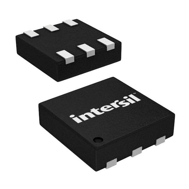
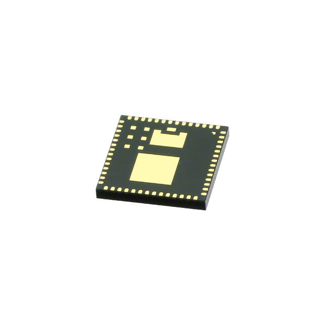
| 产品图片 |
|
| 产品型号 | ISL54503IRUZ-T |
| rohs | 无铅 / 符合限制有害物质指令(RoHS)规范要求 |
| 产品系列 | - |
| 产品培训模块 | http://www.digikey.cn/PTM/IndividualPTM.page?site=cn&lang=zhs&ptm=25476 |
| 供应商器件封装 | 6-UTDFN(1.2x1.0) |
| 其它名称 | ISL54503IRUZ-TDKR |
| 功能 | |
| 包装 | Digi-Reel® |
| 安装类型 | 表面贴装 |
| 导通电阻 | 2.5 欧姆 |
| 封装/外壳 | 6-UFDFN |
| 工作温度 | -40°C ~ 85°C |
| 标准包装 | 1 |
| 电压-电源,单/双 (±) | 1.8 V ~ 5.5 V |
| 电压源 | 单电源 |
| 电流-电源 | 28nA |
| 电路 | 1 x SPDT |


- 商务部:美国ITC正式对集成电路等产品启动337调查
- 曝三星4nm工艺存在良率问题 高通将骁龙8 Gen1或转产台积电
- 太阳诱电将投资9.5亿元在常州建新厂生产MLCC 预计2023年完工
- 英特尔发布欧洲新工厂建设计划 深化IDM 2.0 战略
- 台积电先进制程称霸业界 有大客户加持明年业绩稳了
- 达到5530亿美元!SIA预计今年全球半导体销售额将创下新高
- 英特尔拟将自动驾驶子公司Mobileye上市 估值或超500亿美元
- 三星加码芯片和SET,合并消费电子和移动部门,撤换高东真等 CEO
- 三星电子宣布重大人事变动 还合并消费电子和移动部门
- 海关总署:前11个月进口集成电路产品价值2.52万亿元 增长14.8%


PDF Datasheet 数据手册内容提取
NORTE CROEMCOMMENMDEENDIDS ERLD5E4 PF0LO5A0RC NEEMWE NDTE PSAIGRNTS DATASHEET ISL54503 FN6551 +1.8V to +5.5V, 2.5Ω, Single SPDT Analog Switch Rev 2.00 October 26, 2009 The Intersil ISL54503 device is a low ON-resistance, Features low voltage, bidirectional, single pole/double throw (SPDT) analog switch designed to operate from a • ON-resistance (rON) single +1.8V to +5.5V supply. Targeted applications - VCC = +5.0V . . . . . . . . . . . . . . . . . . . . . 2.5 include battery powered equipment that benefit from - VCC = +3.0V . . . . . . . . . . . . . . . . . . . . . 4.0 low ON-resistance (2.5and fast switching speeds - VCC = +1.8V . . . . . . . . . . . . . . . . . . . . . 7.0 (tON = 25ns, tOFF=15ns). The digital logic input is 1.8V CMOS compatible when using a single +3V • rON matching between channels. . . . . . . . . . . 3m supply. • rON flatness (+4.5V Supply) . . . . . . . . . . . . . 0.6 Cell phones, for example, often face ASIC • Single supply operation. . . . . . . . . +1.8V to +5.5V functionality limitations. The number of analog input • Fast switching action (+4.5V Supply) or GPIO pins may be limited and digital geometries - tON. . . . . . . . . . . . . . . . . . . . . . . . . . . . 25ns are not well suited to analog switch performance. This part may be used to “mux-in” additional functionality - tOFF . . . . . . . . . . . . . . . . . . . . . . . . . . . 15ns while reducing ASIC design risk. The ISL54503 is • Guaranteed break-before-make offered in a 6 Ld 1.2mmx1.0mmx0.4mm pitch µTDFN • ESD HBM rating . . . . . . . . . . . . . . . . . . . . . . . 6kV package and a 6Ld SOT-23 package, alleviating • 1.8V CMOS logic compatible (+3V supply) board space limitations. • Available in 6 Ld µTDFN and 6 Ld SOT-23 packages The ISL54503 is a committed SPDT that consists of • Pb-free available (RoHS compliant) one normally open (NO) and one normally closed (NC) switch. This configuration can also be used as a Applications 2-to-1 multiplexer. • Battery powered, handheld, and portable TABLE 1. FEATURES AT A GLANCE equipment ISL54503 - Cellular/mobile phones Number of Switches 1 - Pagers - Laptops, notebooks, palmtops SW SPDT or 2-1 MUX 1.8V rON 6 • Portable test and measurement • Medical equipment 1.8V tON/tOFF 65ns/40ns • Audio and video switching 3V rON 3 Related Literature 3V tON/tOFF 30ns/20ns • Technical Brief TB363 “Guidelines for Handling and 5V rON 2.5 Processing Moisture Sensitive Surface Mount 5V tON/tOFF 25ns/15ns Devices (SMDs)” Package 6 Ld µTDFN, 6 Ld SOT-23 FN6551 Rev 2.00 Page 1 of 13 October 26, 2009
ISL54503 Ordering Information PACKAGE PART NUMBER PART TEMP. RANGE Tape & Reel PKG. (Notes 1, 4) MARKING (°C) (Pb-Free) DWG. # ISL54503IRUZ-T (Note 2) 3 -40 to +85 6 Ld µTDFN L6.1.2x1.0A ISL54503IHZ-T (Note 3) 4503 -40 to +85 6 Ld SOT-23 MDP0038 1. Please refer to TB347 for details on reel specifications. 2. These Intersil Pb-free plastic packaged products employ special Pb-free material sets; molding compounds/die attach materials and NiPdAu plate - e4 termination finish, which is RoHS compliant and compatible with both SnPb and Pb-free soldering operations. Intersil Pb-free products are MSL classified at Pb-free peak reflow temperatures that meet or exceed the Pb-free requirements of IPC/JEDEC J STD-020. 3. These Intersil Pb-free plastic packaged products employ special Pb-free material sets, molding compounds/die attach materials, and 100% matte tin plate plus anneal (e3 termination finish, which is RoHS compliant and compatible with both SnPb and Pb-free soldering operations). Intersil Pb-free products are MSL classified at Pb-free peak reflow temperatures that meet or exceed the Pb-free requirements of IPC/JEDEC J STD-020. 4. For Moisture Sensitivity Level (MSL), please see device information page for ISL54503. For more information on MSL please see techbrief TB363. Pin Configuration Pin Descriptions (Note 5) ISL54503 PIN PIN (6 LD µTDFN) NAME µTDFN SOT-23 FUNCTION TOP VIEW V+ 5 4 System Power Supply Input (+1.8V to +5.5V) NO 1 6 IN GND 2 6 Ground Connection GND 2 5 V+ IN 6 2 Digital Control Input NC 3 4 COM COM 4 5 Analog Switch Common Pin NO 1 3 Analog Switch Normally Open Pin NC 3 1 Analog Switch Normally Closed Pin ISL54503 (6 LD SOT-23) TOP VIEW NC 1 6 GND IN 2 5 COM NO 3 4 V+ NOTE: 5. Switches Shown for Logic “0” Input. Truth Table LOGIC PIN NC PIN NO 0 ON OFF 1 OFF ON NOTE: Logic “0” 0.5V. Logic “1” 1.4V with a 3V supply. FN6551 Rev 2.00 Page 2 of 13 October 26, 2009
ISL54503 Absolute Maximum Ratings Thermal Information V+ to GND . . . . . . . . . . . . . . . . . . . . . . . . . . -0.5 to 6.5V Thermal Resistance (Typical) JA (°C/W) JC (°C/W) Input Voltages 6 Ld µTDFN Package (Notes 7, 9). . 239.2 111.6 NO, NC, IN (Note 6). . . . . . . . . . . -0.5V to ((V+) + 0.5V) 6 Ld SOT-23 Package (Note 8, 9). . 260 120 Output Voltages Maximum Junction Temperature (Plastic Package). . +150°C COM (Note 6) . . . . . . . . . . . . . . . -0.5V to ((V+) + 0.5V) Maximum Storage Temperature Range. . . . . -65°C to +150°C Continuous Current NO, NC, or COM. . . . . . . . . . . . 300mA Pb-Free Reflow Profile . . . . . . . . . . . . . . . . . .see link below Peak Current NO, NC, or COM http://www.intersil.com/pbfree/Pb-FreeReflow.asp (Pulsed 1ms, 10% Duty Cycle, Max) . . . . . . . . . . 500mA ESD Rating Recommended Operating Conditions Human Body Model . . . . . . . . . . . . . . . . . . . . . . . . >6kV Machine Model . . . . . . . . . . . . . . . . . . . . . . . . . . >300V V+ (Positive DC Supply Voltage). . . . . . . . . . . 1.8V to 5.5V Charged Device Model . . . . . . . . . . . . . . . . . . . . . .>2.2kV Analog Signal Range . . . . . . . . . . . . . . . . . . . . . . 0V to V+ VIN (Digital Logic Input Voltage (IN) . . . . . . . . . . . 0V to V+ Temperature Range. . . . . . . . . . . . . . . . . . -40°C to +85°C CAUTION: Do not operate at or near the maximum ratings listed for extended periods of time. Exposure to such conditions may adversely impact product reliability and result in failures not covered by warranty. NOTES: 6. Signals on NC, NO, IN, or COM exceeding V+ or GND are clamped by internal diodes. Limit forward diode current to maximum current ratings. 7. JA is measured in free air with the component mounted on a high effective thermal conductivity test board with “direct attach” features. See Tech Brief TB379. 8. JA is measured with the component mounted on a high effective thermal conductivity test board in free air. See Tech Brief TB379 for details. 9. For JC, the “case temp” location is the center of the exposed metal pad on the package underside. Electrical Specifications - 5V Supply Test Conditions: V+ = +4.5V to +5.5V, GND = 0V, VINH = 2.0V, VINL = 0.8V (Note10), Unless Otherwise Specified. Boldface limits apply over the operating temperature range, -40°C to +85°C. TEMP MIN MAX PARAMETER TEST CONDITIONS (°C) (Notes 11, 12) TYP (Notes 11, 12) UNITS ANALOG SWITCH CHARACTERISTICS Analog Signal Range, Full 0 - V+ V VANALOG ON-Resistance, rON V+ = 4.5V, ICOM = 100mA, VNO or VNC = 0V 25 - 2.2 2.5 to V+, (Note 14, See Figure 5) Full - - 3 rON Matching Between V+ = 4.5V, ICOM = 100mA, VNO or 25 - 0.003 0.1 Channels, rON VNC=2.5V (Note 14) Full - - 0.15 rON Flatness, rFLAT(ON) V+ = 4.5V, ICOM = 100mA, VNO or VNC = 0V 25 - 0.6 0.65 to V+, (Notes 13, 14) Full - - 0.7 NO or NC OFF Leakage V+ = 5.5V, VCOM = 0.3V, 5V, VNO or 25 -25 1.5 25 nA Current, INO(OFF) or VNC=5V, 0.3V Full -150 - 150 nA INC(OFF) COM ON Leakage Current, V+ = 5.5V, VCOM = 0.3V, 5V, or VNO or 25 -30 2.8 30 nA ICOM(ON) VNC= 0.3V, 5V, or Floating Full -300 - 300 nA DYNAMIC CHARACTERISTICS Turn-ON Time, tON V+ = 4.5V, VNO or VNC = 3.0V, RL = 50, 25 - 25 - ns CL = 35pF (see Figure 1, Note 14) Full - 25 - ns Turn-OFF Time, tOFF V+ = 4.5V, VNO or VNC = 3.0V, RL = 50, 25 - 15 - ns CL = 35pF (see Figure 1, Note 14) Full - 16 - ns Break-Before-Make Time V+ = 5.5V, VNO or VNC = 3.0V, RL = 50, Full - 15 - ns Delay, tD CL = 35pF (see Figure 3, Note 14) Charge Injection, Q VG = 0V, RG = 0, CL = 1.0nF (see Figure 2) 25 - 24 - pC OFF-Isolation RL = 50, CL = 5pF, f = 1MHz, 25 - 70 - dB VCOM=1VP-P (see Figure 4) FN6551 Rev 2.00 Page 3 of 13 October 26, 2009
ISL54503 Electrical Specifications - 5V Supply Test Conditions: V+ = +4.5V to +5.5V, GND = 0V, VINH = 2.0V, VINL = 0.8V (Note10), Unless Otherwise Specified. Boldface limits apply over the operating temperature range, -40°C to +85°C. (Continued) TEMP MIN MAX PARAMETER TEST CONDITIONS (°C) (Notes 11, 12) TYP (Notes 11, 12) UNITS Total Harmonic Distortion f = 20Hz to 20kHz, VCOM = 2VP-P, RL = 32 25 - 0.15 - % Total Harmonic Distortion f = 20Hz to 20kHz, VCOM = 2VP-P, 25 - 0.014 - % RL=600 -3dB Bandwidth RL = 50 25 - 250 - MHz NO or NC OFF Capacitance, V+ = 4.5V, f = 1MHz, VNO or VNC = VCOM = 25 - 7 - pF COFF 0V (see Figure 7) COM ON Capacitance, V+ = 4.5V, f = 1MHz, VNO or VNC = VCOM = 25 - 18 - pF CCOM(ON) 0V (see Figure 7) POWER SUPPLY CHARACTERISTICS Power Supply Range Full 1.65 - 5.5 V Positive Supply Current, I+ V+ = 5.5V, VIN = 0V or V+ 25 - 0.028 0.1 µA Full - 1.1 2.5 µA DIGITAL INPUT CHARACTERISTICS Input Voltage Low, VINL Full - - 0.8 V Input Voltage High, VINH Full 2.4 - - V Input Current, IINH, IINL V+ = 5.5V, VIN = 0V or V+ Full -0.1 0.053 0.1 µA Electrical Specifications - 3V Supply Test Conditions: V+ = +2.7V to +3.6V, GND = 0V, VINH = 1.4V, VINL = 0.5V (Note10), Unless Otherwise Specified. Boldface limits apply over the operating temperature range, -40°C to +85°C. TEMP MIN MAX PARAMETER TEST CONDITIONS (°C) (Notes 11, 12) TYP (Notes 11, 12) UNITS ANALOG SWITCH CHARACTERISTICS Analog Signal Range, Full 0 - V+ V VANALOG ON-Resistance, rON V+ = 2.7V, ICOM = 100mA, VNO or VNC = 0V 25 - 3.3 3.5 µTDFN to V+, (Note 14, See Figure 5) Full - - 4.5 ON-Resistance, rON V+ = 2.7V, ICOM = 100mA, VNO or VNC = 0V 25 - 3.3 3.6 SOT-23 to V+, (Note 14, See Figure 5) Full - - 4.5 rON Matching Between V+ = 2.7V, ICOM = 100mA, VNO or 25 - 0.006 0.15 Channels, VNC=1.5V (Note 14) Full - - 0.2 rON rON Flatness, rFLAT(ON) V+ = 2.7V, ICOM = 100mA, VNO or VNC = 0V 25 - 1 1.1 µTDFN to V+, (Notes 13, 14) Full - - 1.2 rON Flatness, rFLAT(ON) V+ = 2.7V, ICOM = 100mA, VNO or VNC = 0V 25 - 1 1.2 SOT-23 to V+, (Notes 13, 14) Full - - 1.3 DYNAMIC CHARACTERISTICS Turn-ON Time, tON V+ = 2.7V, VNO or VNC = 1.5V, RL = 50, 25 - 30 - ns CL = 35pF (see Figure 1, Note 14) Full - 30 - ns Turn-OFF Time, tOFF V+ = 2.7V, VNO or VNC = 1.5V, RL = 50, 25 - 20 - ns CL = 35pF (see Figure 1, Note 14) Full - 20 - ns Break-Before-Make Time V+ = 3.0V, VNO or VNC = 1.5V, RL = 50, Full - 18 - ns Delay, tD CL = 35pF (see Figure 3, Note 14) Charge Injection, Q VG = 0V, RG = 0, CL = 1.0nF (see Figure 2) 25 - 16 - pC OFF-Isolation RL = 50, CL = 5pF, f = 1MHz, VCOM = 25 - 70 - dB 1VP-P (see Figure 4) Total Harmonic Distortion f = 20Hz to 20kHz, VCOM = 2VP-P, RL = 32 25 - 0.36 - % FN6551 Rev 2.00 Page 4 of 13 October 26, 2009
ISL54503 Electrical Specifications - 3V Supply Test Conditions: V+ = +2.7V to +3.6V, GND = 0V, VINH = 1.4V, VINL = 0.5V (Note10), Unless Otherwise Specified. Boldface limits apply over the operating temperature range, -40°C to +85°C. (Continued) TEMP MIN MAX PARAMETER TEST CONDITIONS (°C) (Notes 11, 12) TYP (Notes 11, 12) UNITS Total Harmonic Distortion f = 20Hz to 20kHz, VCOM = 2VP-P, 25 - 0.03 - % RL=600 -3dB Bandwidth Signal = 0dBm, RL = 50 25 - 250 - MHz NO or NC OFF Capacitance, f = 1MHz, VNO or VNC = VCOM = 0V 25 - 6 - pF COFF (seeFigure 7) COM ON Capacitance, f = 1MHz, VNO or VNC = VCOM = 0V 25 - 18 - pF CCOM(ON) (seeFigure 7) POWER SUPPLY CHARACTERISTICS Positive Supply Current, I+ V+ = 3.6V, VIN = 0V or V+ 25 - 0.013 - µA Full - 0.7 - µA DIGITAL INPUT CHARACTERISTICS Input Voltage Low, VINL Full - - 0.5 V Input Voltage High, VINH Full 1.4 - - V Input Current, IINH, IINL V+ = 3.6V, VIN = 0V or V+ Full -0.1 0.058 0.1 µA Electrical Specifications - 1.8V Supply Test Conditions: V+ = +1.8V, GND = 0V, VINH = 1V, VINL = 0.4V (Note 10), Unless Otherwise Specified. Boldface limits apply over the operating temperature range, -40°C to +85°C. TEMP MIN MAX PARAMETER TEST CONDITIONS (°C) (Notes 11, 12) TYP (Notes 11, 12) UNITS ANALOG SWITCH CHARACTERISTICS Analog Signal Range, Full 0 - V+ V VANALOG ON-Resistance, rON V+ = 1.8V, ICOM = 10mA, VNO or VNC = 0V 25 - 6 6.5 to V+, (Note 14, See Figure 5) Full - - 7 DYNAMIC CHARACTERISTICS Turn-ON Time, tON V+ = 1.8V, VNO or VNC = 1.5V, RL = 50, 25 - 65 - ns CL= 35pF (see Figure 1, Note 14) Full - 95 - ns Turn-OFF Time, tOFF V+ = 1.8V, VNO or VNC = 1.5V, RL = 50, 25 - 40 - ns CL= 35pF (see Figure 1, Note 14) Full - 65 - ns Break-Before-Make Time V+ = 1.8V, VNO or VNC = 1.5V, RL = 50, Full - 44 - ns Delay, tD CL= 35pF (see Figure 3, Note 14) Charge Injection, Q VG = 0, RG = 0CL = 1.0nF (see Figure 2) 25 - 8.2 - pC DIGITAL INPUT CHARACTERISTICS Input Voltage Low, VINL Full - - 0.4 V Input Voltage High, VINH Full 1 - - V NOTES: 10. VIN = input voltage to perform proper function. 11. The algebraic convention, whereby the most negative value is a minimum and the most positive a maximum, is used in this data sheet. 12. Parameters with MIN and/or MAX limits are 100% tested at +25°C, unless otherwise specified. Temperature limits established by characterization and are not production tested. 13. Flatness is defined as the difference between maximum and minimum value of on-resistance over the specified analog signal range. 14. Limits established by characterization and are not production tested. FN6551 Rev 2.00 Page 5 of 13 October 26, 2009
ISL54503 Test Circuits and Waveforms V+ tr < 20ns V+ C LOGIC 50% tf < 20ns INPUT 0V tOFF NO OR NC VOUT SWITCH SWITCH INPUT COM INPUTVNO VOUT IN 90% 90% SWITCH LOGIC GND RL CL OUTPUT 0V INPUT 50 35pF tON Logic input waveform is inverted for switches that have the Repeat test for all switches. CL includes fixture and stray opposite logic sense. capacitance. R L V = V ------------------------ OUT (NO or NC) R +r L ON FIGURE 1A. MEASUREMENT POINTS FIGURE 1B. TEST CIRCUIT FIGURE 1. SWITCHING TIMES V+ C SOWUTITPCUHT VOUT RG NO OR NC COM VOUT VOUT VINH LOGIC ON ON VG GND IN INPUT OFF CL VINL LOGIC INPUT Q = VOUT x CL FIGURE 2A. MEASUREMENT POINTS FIGURE 2B. TEST CIRCUIT FIGURE 2. CHARGE INJECTION V+ C NO V+ LOGIC VNX COM VOUT INPUT NC 0V RL CL IN 50 35pF LOGIC GND SWITCH 90% INPUT OUTPUT VOUT 0V tD CL includes fixture and stray capacitance. FIGURE 3A. MEASUREMENT POINTS FIGURE 3B. TEST CIRCUIT FIGURE 3. BREAK-BEFORE-MAKE TIME FN6551 Rev 2.00 Page 6 of 13 October 26, 2009
ISL54503 Test Circuits and Waveforms (Continued) V+ V+ C C rON = V1/I1 * SIGNAL GENERATOR NO OR NC NO OR NC VNX IN 0V OR V+ I1 V1 IN VINL OR VINH 100mA COM COM ANALYZER GND GND RL * I1 = 10mA AT V+ = 1.8V FIGURE 4. OFF-ISOLATION TEST CIRCUIT FIGURE 5. rON TEST CIRCUIT V+ V+ C C NO OR NC 50 NO OR NC COM IN VINL OR VINH IN1 IMPEDANCE SIGNAL ANALYZER 0V OR V+ GENERATOR COM GND NC OR NO ANALYZER GND RL FIGURE 6. CROSSTALK TEST CIRCUIT FIGURE 7. CAPACITANCE TEST CIRCUIT Detailed Description parasitic SCR structures to turn ON, creating a low impedance path from the V+ power supply to ground. The ISL54503 is a bi-directional, single pole/double This will result in a significant amount of current flow in throw (SPDT) analog switch that offers precise the IC, which can potentially create a latch-up state or switching capability from a single 1.8V to 5.5V supply permanently damage the IC. The external V+ resistor with low ON-resistance (2.5) and high speed limits the current during this over-stress situation and operation (tON = 25ns, tOFF = 15ns). The device is has been found to prevent latch-up or destructive especially well suited for portable battery powered damage for many overvoltage transient events. equipment due to its low operating supply voltage (1.8V), low power consumption (0.15µW), low Under normal operation, the sub-microamp IDD leakage currents (300nA max), and the small µTDFN current of the IC produces an insignificant voltage drop and SOT-23 packages. The low ON-resistance and rON across the 100 series resistor resulting in no impact flatness provide very low insertion loss and distortion to switch operation or performance. to application that require signal reproduction. External V+ Series Resistor For improved ESD and latch-up immunity Intersil recommends adding a 100 resistor in series with the V+ power supply pin of the ISL54050 IC (seeFigure8). During an overvoltage transient event (such as occurs during system level IEC 61000 ESD testing), substrate currents can be generated in the IC that can trigger FN6551 Rev 2.00 Page 7 of 13 October 26, 2009
ISL54503 V+ C OPTIONAL SCHOTTKY OPTIONAL DIODE PROTECTION RESISTOR 100 V+ OPTIONAL PROTECTION NO RESISTOR INX COM NC VNX VCOM IN GND GND OPTIONAL SCHOTTKY DIODE FIGURE 8. V+ SERIES RESISTOR FOR ENHANCED ESD AND LATCH-UP IMMUNITY FIGURE 9. OVERVOLTAGE PROTECTION Supply Sequencing And Overvoltage Power-Supply Considerations Protection The ISL54503 construction is typical of most single With any CMOS device, proper power supply supply CMOS analog switches, in that they have two sequencing is required to protect the device from supply pins: V+ and GND. V+ and GND drive the excessive input currents, which might permanently internal CMOS switches and set their analog voltage damage the IC. All I/O pins contain ESD protection limits. Unlike switches with a 4V maximum supply diodes from the pin to V+ and to GND (see Figure 9). voltage, the ISL54503 5.5V maximum supply voltage To prevent forward biasing these diodes, V+ must be provides plenty of room for the 10% tolerance of 3.6V applied before any input signals, and the input signal supplies, as well as room for overshoot and noise voltages must remain between V+ and GND. spikes. If these conditions cannot be guaranteed then The minimum recommended supply voltage is 1.8V but precautions must be implemented to prohibit the the part will operate with a supply below 1.8V. It is current and voltage at the logic pin and signal pins important to note that the input signal range, switching from exceeding the maximum ratings of the switch. times, and ON-resistance degrade at lower supply The following two methods can be used to provide voltages. Refer to the “Electrical Specifications” tables additional protection to limit the current in the event starting on page3 and the “Typical Performance that the voltage at a signal pin or logic pin goes below Curves” starting on page10 for details. ground or above the V+ rail. V+ and GND also power the internal logic and level Logic inputs can easily be protected by adding a 1k shifters. The level shifters convert the input logic levels resistor in series with the input (see Figure 9). The to switched V+ and GND signals to drive the analog resistor limits the input current below the threshold switch gate terminals. that produces permanent damage, and the This family of switches cannot be operated with bipolar sub-microamp input current produces an insignificant supplies, because the input switching point becomes voltage drop during normal operation. negative in this configuration. This method is not acceptable for the signal path Logic-Level Thresholds inputs. Adding a series resistor to the switch input defeats the purpose of using a low rON switch. This switch family is 1.8V CMOS compatible (0.5V and Connecting Schottky diodes to the signal pins (as 1.4V) over a supply range of 2V to 3.6V (see shown in Figure 9) will shunt the fault current to the Figure16). At 3.6V the VIH level is about 0.95V. This is supply or to ground, thereby protecting the switch. still below the 1.8V CMOS guaranteed high output These Schottky diodes must be sized to handle the minimum level of 1.4V, but noise margin is reduced. expected fault current. The digital input stages draw supply current whenever the digital input voltage is not at one of the supply rails. Driving the digital input signals from GND to V+ with a fast transition time minimizes power dissipation. High-Frequency Performance In 50 systems, the ISL54503 has a -3dB bandwidth of 250MHz (see Figure 17). The frequency response is very consistent over a wide V+ range, and for varying analog signal levels. FN6551 Rev 2.00 Page 8 of 13 October 26, 2009
ISL54503 An OFF switch behaves like a capacitor and passes higher frequencies with less attenuation, resulting in signal feed-through from a switch’s input to output. Off-isolation is the resistance of this signal feed-through. Figure 18 details the high off-isolation provided by the ISL54503. At 1MHz, off-isolation is about 70dB in 50 systems, decreasing approximately 20dB per decade as frequency increases. Higher load impedances decrease off-isolation due to the voltage divider action of the switch OFF impedance and the load impedance. Leakage Considerations ESD protection diodes are internally connected between each analog-signal pin and both V+ and GND. One of these diodes conducts if any analog signal exceeds V+ or GND. Virtually all the analog leakage current comes from the ESD diodes to V+ or GND. Although the ESD diodes on a given signal pin are identical and therefore fairly well balanced, they are reverse biased differently. Each is biased by either V+ or GND and the analog signal. This means their leakages will vary as the signal varies. The difference in the two diode leakages to the V+ and GND pins constitutes the analog-signal-path leakage current. All analog leakage current flows between each pin and one of the supply terminals, not to the other switch terminal. This is why both sides of a given switch can show leakage currents of the same or opposite polarity. There is no connection between the analog signal paths and V+ or GND. FN6551 Rev 2.00 Page 9 of 13 October 26, 2009
ISL54503 Typical Performance Curves TA = 25°C, Unless Otherwise Specified 4.0 3.0 ICOM = 100mA 3.5 2.5 V+ = 2.7V 3.0 +85°C V+ = 3V 2.0 2.5 +25°C ) ) (N 2.0 V+ = 4.5V (N 1.5 -40°C O O r r 1.5 V+ = 5V 1.0 1.0 V+ = 4.5V 0.5 0.5 ICOM = 100mA 0.0 0.0 0 1 2 3 4 5 0 0.5 1.0 1.5 2.0 2.5 3.0 3.5 4.0 4.5 VCOM (V) VCOM (V) FIGURE 10. ON-RESISTANCE vs SUPPLY VOLTAGE vs FIGURE 11. ON-RESISTANCE vs SWITCH VOLTAGE SWITCH VOLTAGE 5.0 8 V+ = 2.7V V+ = 1.8V 4.5 ICOM = 100mA 7 ICOM = 10mA 4.0 6 +85°C 3.5 ) +85°C ) 5 (ON 3.0 +25°C (ON +25°C r r 4 2.5 -40°C -40°C 3 2.0 2 1.5 1.0 1 0 0.5 1.0 1.5 2.0 2.5 0 0.2 0.4 0.6 0.8 1.0 1.2 1.4 1.6 1.8 2.0 VCOM (V) VCOM (V) FIGURE 12. ON-RESISTANCE vs SWITCH VOLTAGE FIGURE 13. ON-RESISTANCE vs SWITCH VOLTAGE 100 70 -40°C 90 -40°C 60 80 70 +25°C 50 +25°C 60 (ns)tON 4500 +85°C t (ns)OFF 3400 +85°C 30 20 20 10 10 0 0 1.5 2.0 2.5 3.0 3.5 4.0 4.5 5.0 5.5 6.0 1.5 2.0 2.5 3.0 3.5 4.0 4.5 5.0 5.5 6.0 V+ (V) V+ (V) FIGURE 14. TURN-ON TIME vs SUPPLY VOLTAGE FIGURE 15. TURN-OFF TIME vs SUPPLY VOLTAGE FN6551 Rev 2.00 Page 10 of 13 October 26, 2009
ISL54503 Typical Performance Curves TA = 25°C, Unless Otherwise Specified (Continued) 1.4 0 -1 1.2 -2 V+ = 1.8V TO 5.5V B) -3 VCOM = 1VP-P d V) 1.0 N ( -4 ( I NL GA -5 VI VINH D -6 D 0.8 ZE N I -7 AH VINL MAL -8 VIN 0.6 OR -9 N -10 0.4 -11 -12 0.2 -13 1.5 2.0 2.5 3.0 3.5 4.0 4.5 5.0 5.5 100k 1M 10M 100M 1G V+ (V) FREQUENCY (Hz) FIGURE 16. DIGITAL SWITCHING POINT vs SUPPLY FIGURE 17. FREQUENCY RESPONSE VOLTAGE -20 25 V+ = 1.8V TO 5.5V -30 20 -40 15 -50 10 -60 (dB)-70 Q (pC) 05 -80 V+ = 5V -5 -90 V+ = 1.8V V+ = 3.3V -10 -100 -15 -110 -120 -20 1k 10k 100k 1M 10M 100M 1G 0.0 0.5 1.0 1.5 2.0 2.5 3.0 3.5 4.0 4.5 5.0 FREQUENCY (Hz) VCOM (V) FIGURE 18. OFF-ISOLATION FIGURE 19. CHARGE INJECTION vs SWITCH VOLTAGE Die Characteristics SUBSTRATE POTENTIAL (POWERED UP): GND TRANSISTOR COUNT: PROCESS: Submicron CMOS FN6551 Rev 2.00 Page 11 of 13 October 26, 2009
ISL54503 Ultra Thin Dual Flat No-Lead Plastic Package (UTDFN) L6.1.2x1.0A E A B 6 LEAD ULTRA THIN DUAL FLAT NO-LEAD PLASTIC PACKAGE MILLIMETERS PIN 1 D NOMI- REFERENCE SYMBOL MIN NAL MAX NOTES 2X 0.10C A 0.45 0.50 0.55 - 2X 0.10C A1 - - 0.05 - TOP VIEW A3 0.127 REF - DETAIL A b 0.15 0.20 0.25 5 0.10C D 0.95 1.00 1.05 - A 7X 0.08C E 1.15 1.20 1.25 - A1 A3 C e 0.40 BSC - SEATING SIDE VIEW PLANE L 0.30 0.35 0.40 - L1 0.40 0.45 0.50 - DETAIL B 4X e N 6 2 5X 1 3 L Ne 3 3 L1 0 - 12 4 Rev. 2 8/06 NOTES: 6 4 1. Dimensioning and tolerancing conform to ASME Y14.5- b 6X 1994. 0.10 C A B 0.05C NOTE 3 2. N is the number of terminals. BOTTOM VIEW 3. Ne refers to the number of terminals on E side. 4. All dimensions are in millimeters. Angles are in degrees. 0.1x45° 5. Dimension b applies to the metallized terminal and is CHAMFER measured between 0.15mm and 0.30mm from the terminal tip. 6. The configuration of the pin #1 identifier is optional, but must be located within the zone indicated. The pin #1 identifier may be either a mold or mark feature. A1 A3 7. Maximum package warpage is 0.05mm. DETAIL A DETAIL B PIN 1 LEAD 8. Maximum allowable burrs is 0.076mm in all directions. 9. JEDEC Reference MO-255. 10. For additional information, to assist with the PCB Land Pattern Design effort, see Intersil Technical Brief TB389. 1.00 1.40 0.20 0.30 0.45 0.35 0.20 0.40 LAND PATTERN 10 FN6551 Rev 2.00 Page 12 of 13 October 26, 2009
ISL54503 SOT-23 Package Family MDP0038 e1 D SOT-23 PACKAGE FAMILY A MILLIMETERS 6 N 4 SYMBOL SOT23-5 SOT23-6 TOLERANCE A 1.45 1.45 MAX A1 0.10 0.10 ±0.05 E1 E A2 1.14 1.14 ±0.15 2 3 b 0.40 0.40 ±0.05 0.15 C D c 0.14 0.14 ±0.06 2X 1 2 3 0.20 C D 2.90 2.90 Basic 5 e 2X E 2.80 2.80 Basic E1 1.60 1.60 Basic B 0.20M C A-B D b e 0.95 0.95 Basic NX e1 1.90 1.90 Basic L 0.45 0.45 ±0.10 L1 0.60 0.60 Reference 0.15 C A-B 1 3 N 5 6 Reference 2X D Rev. F 2/07 NOTES: C 1. Plastic or metal protrusions of 0.25mm maximum per side are not A2 included. SEATING 2. Plastic interlead protrusions of 0.25mm maximum per side are not PLANE included. A1 0.10 C 3. This dimension is measured at Datum Plane “H”. NX 4. Dimensioning and tolerancing per ASME Y14.5M-1994. 5. Index area - Pin #1 I.D. will be located within the indicated zone (SOT23-6 only). 6. SOT23-5 version has no center lead (shown as a dashed line). (L1) H A GAUGE PLANE 0.25 c L 0°+-03°° © Copyright Intersil Americas LLC 2007-2009. All Rights Reserved. All trademarks and registered trademarks are the property of their respective owners. For additional products, see www.intersil.com/en/products.html Intersil products are manufactured, assembled and tested utilizing ISO9001 quality systems as noted in the quality certifications found at www.intersil.com/en/support/qualandreliability.html Intersil products are sold by description only. Intersil may modify the circuit design and/or specifications of products at any time without notice, provided that such modification does not, in Intersil's sole judgment, affect the form, fit or function of the product. Accordingly, the reader is cautioned to verify that datasheets are current before placing orders. Information furnished by Intersil is believed to be accurate and reliable. However, no responsibility is assumed by Intersil or its subsidiaries for its use; nor for any infringements of patents or other rights of third parties which may result from its use. No license is granted by implication or otherwise under any patent or patent rights of Intersil or its subsidiaries. For information regarding Intersil Corporation and its products, see www.intersil.com FN6551 Rev 2.00 Page 13 of 13 October 26, 2009