ICGOO在线商城 > 开发板,套件,编程器 > 评估和演示板和套件 > ISD-DEMO3800
 Datasheet下载
- 型号: ISD-DEMO3800
- 制造商: Nuvoton Technology Corporation of America
- 库位|库存: xxxx|xxxx
- 要求:
| 数量阶梯 | 香港交货 | 国内含税 |
| +xxxx | $xxxx | ¥xxxx |
查看当月历史价格
查看今年历史价格
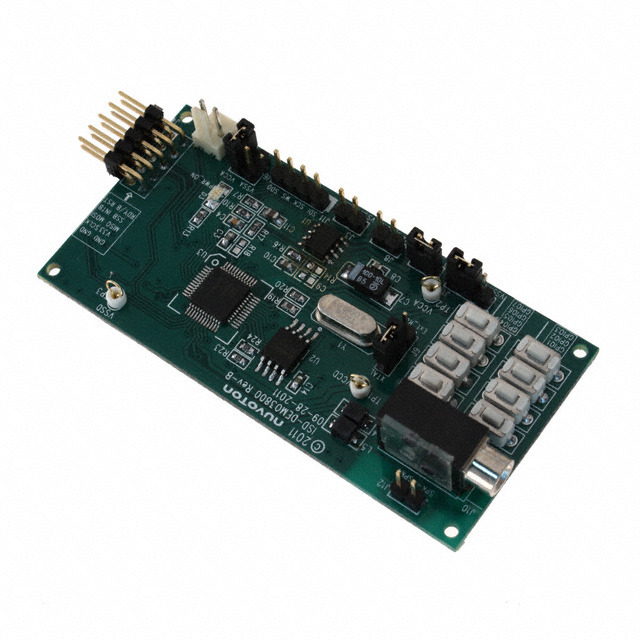
ISD-DEMO3800产品简介:
ICGOO电子元器件商城为您提供ISD-DEMO3800由Nuvoton Technology Corporation of America设计生产,在icgoo商城现货销售,并且可以通过原厂、代理商等渠道进行代购。 ISD-DEMO3800价格参考。Nuvoton Technology Corporation of AmericaISD-DEMO3800封装/规格:评估和演示板和套件, ISD3800 录音/回放 音频 Evaluation Board。您可以下载ISD-DEMO3800参考资料、Datasheet数据手册功能说明书,资料中有ISD-DEMO3800 详细功能的应用电路图电压和使用方法及教程。
Nuvoton Technology Corporation of America推出的ISD-DEMO3800是一款专为ISD系列语音芯片设计的评估与演示开发套件,主要用于快速评估和开发高质量语音录放应用。该套件广泛应用于需要嵌入式语音功能的产品研发阶段,帮助工程师测试语音录制、存储、播放及多段语音触发等核心功能。

典型应用场景包括:智能家居设备(如语音提示门铃、智能家电语音反馈)、消费类电子产品(如儿童教育玩具、电子贺卡)、工业控制系统(如设备故障语音报警)、医疗设备(如便携仪器操作提示)以及安防系统(如语音警示装置)。通过ISD-DEMO3800,开发者可便捷地验证Nuvoton ISD芯片的性能,进行音频质量评估、存储管理测试和GPIO控制逻辑调试,从而加速产品原型设计与量产进程。

该套件支持多种音频输入输出方式,配备基本按键与接口,便于用户快速上手并实现即插即用的演示效果。同时,配套软件工具简化了语音内容烧录与配置流程,适合研发初期的功能验证与客户演示。总体而言,ISD-DEMO3800是面向语音嵌入式系统开发的重要工具平台,适用于各类需要低成本、高可靠性语音解决方案的行业应用。
| 参数 | 数值 |
| 产品目录 | 编程器,开发系统 |
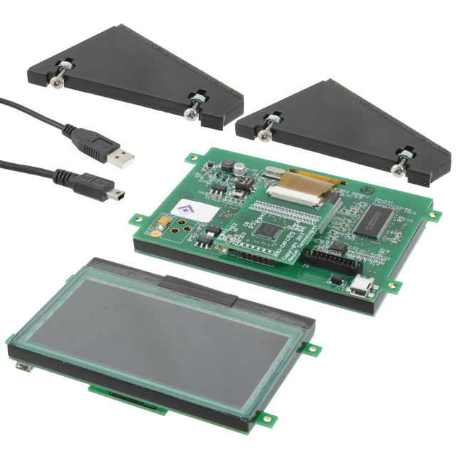
| 描述 | BOARD DEMO FOR ISD3800 |
| 产品分类 | |
| 品牌 | Nuvoton Technology Corporation of America |
| 数据手册 | |
| 产品图片 |
|
| 产品型号 | ISD-DEMO3800 |
| rohs | 无铅 / 符合限制有害物质指令(RoHS)规范要求 |
| 产品系列 | ChipCorder® |
| 主要属性 | - |
| 主要用途 | 音频,语音录制/回放 |
| 使用的IC/零件 | ISD3800 |
| 其它名称 | ISDDEMO3800 |
| 嵌入式 | 否 |
| 所含物品 | 板 |
| 标准包装 | 1 |
| 辅助属性 | - |


- 商务部:美国ITC正式对集成电路等产品启动337调查
- 曝三星4nm工艺存在良率问题 高通将骁龙8 Gen1或转产台积电
- 太阳诱电将投资9.5亿元在常州建新厂生产MLCC 预计2023年完工
- 英特尔发布欧洲新工厂建设计划 深化IDM 2.0 战略
- 台积电先进制程称霸业界 有大客户加持明年业绩稳了
- 达到5530亿美元!SIA预计今年全球半导体销售额将创下新高
- 英特尔拟将自动驾驶子公司Mobileye上市 估值或超500亿美元
- 三星加码芯片和SET,合并消费电子和移动部门,撤换高东真等 CEO
- 三星电子宣布重大人事变动 还合并消费电子和移动部门
- 海关总署:前11个月进口集成电路产品价值2.52万亿元 增长14.8%

PDF Datasheet 数据手册内容提取
ISD3800 DATASHEET ISD3800 Digital ChipCorder with Digital Audio Interface Publication Release Date: Aug 23, 2013 - 1 - Revision 1.0
ISD3800 DATASHEET TABLE OF CONTENTS 1 GENERAL DESCRIPTION .............................................................................................................. 3 2 FEATURES ...................................................................................................................................... 3 3 BLOCK DIAGRAM ........................................................................................................................... 5 4 PINOUT CONFIGURATION ............................................................................................................ 6 4.1 48L-LQFP ................................................................................................................................................ 6 5 PIN DESCRIPTION .......................................................................................................................... 7 6 ELECTRICAL CHARACTERISTICS .............................................................................................. 11 6.1 OPERATING CONDITIONS ........................................................................................................................ 11 6.2 DC PARAMETERS ................................................................................................................................... 12 6.3 AC PARAMETERS ................................................................................................................................... 13 6.3.1 Inputs ............................................................................................................................................. 13 6.3.2 Outputs ........................................................................................................................................... 15 6.3.3 SPI Timing ..................................................................................................................................... 18 6.3.4 I2S Timing ...................................................................................................................................... 19 7 APPLICATION DIAGRAM .............................................................................................................. 21 8 PACKAGE SPECIFICATION ......................................................................................................... 23 8.1 48 LEAD LQFP(7X7X1.4MM FOOTPRINT 2.0MM) .................................................................................... 23 9 ORDERING INFORMATION .......................................................................................................... 24 10 REVISION HISTORY.................................................................................................................. 25 Publication Release Date: Aug 23, 2013 - 2 - Revision 1.0
ISD3800 DATASHEET 1 GENERAL DESCRIPTION The ISD3800 is a digital ChipCorder® featuring digital compression, comprehensive memory management, and integrated analog/digital audio signal paths. The ISD3800 utilizes serial flash memory to provide non-volatile audio playback for a two-chip solution. The ISD3800 provides an I2S digital audio interface, faster digital programming, higher sampling frequency, and a signal path with SNR 80dB. The ISD3800 can take digital audio data via I2S or SPI interface. When I2S input is selected, it will replace the analog audio inputs and will support sample rates of 32, 44.1 or 48 kHz depending upon clock configuration. When SPI interface is chosen, the sample rate of the audio data sent must be one of the ISD3800 supported sample rates. The ISD3800 has inbuilt analog audio inputs, analog audio line driver, and speaker driver output. The analog audio input, Aux-in, has a fixed gain configured by SPI command. Aux-in can directly feed-through to the analog outputs; it can also mix with the DAC output and then feed-through to the analog outputs. Analog outputs are available in two forms: (1) Aux-out is an analog single-ended voltage output; (2) Class-AB BTL (bridge-tied-load) is an analog differential voltage output. Class-AB BTL delivers 1-watt output power at V = 5V. CCSPK Class-D PWM direct-drive is also available, which delivers 1-watt output power at V = 5V. CCSPK 2 FEATURES External Memory: o The ISD3800 supports the following flash: Manufacturer Winbond Numonyx MXIC Family 25X 25Q 25P 25PX 25PE 25L / 25V JEDEC ID EF 30 1X EF 40 1X 20 20 1X 20 71 1X 20 80 1X C2 20 1X o The addressing ability of ISD3800 is up to 128Mbit, which is 64-minute playback time based on 8kHz/4bit ADPCM. o Inbuilt 3V voltage regulator to provide power source to the external flash memory Fast Digital Programming o Programming rate can go up to 1Mbits/second mainly limited by the flash memory write rate. Memory Management o Store pre-recorded audio (Voice Prompts) using high quality digital compression o Use a simple index-based command for playback o Execute pre-programmed macro scripts (Voice Macros) designed to control the configuration of the device and play back Voice Prompts sequences. Sample Rate o Seven sampling frequencies are available for a given master sample rate. For example, the sampling frequencies of 4, 5.3, 6.4, 8, 12.8, 16 and 32kHz are available when the device is clocked at a 32kHz master sample rate. o For I2S operation, 32, 44.1 and 48kHz master sample rates are available with playback sampling frequencies scaling accordingly. Compression Algorithms o For Pre-Recorded Voice Prompts µ-Law: 6, 7 or 8 bits per sample Publication Release Date: Aug 23, 2013 - 3 - Revision 1.0
ISD3800 DATASHEET Differential µ-Law: 6, 7 or 8 bits per sample PCM: 8, 10 or 12 bits per sample Enhanced ADPCM: 2, 3, 4 or 5 bits per sample Variable-bit-rate optimized compression. This allows best possible compression given a metric of SNR and background noise levels. Oscillator o Internal oscillator with internal reference: 2.048 MHz with ±1% deviation o Internal oscillator with external resistor: 2.048 MHz with ±2% deviation1 o External crystal or clock input Crystals support standard audio sampling rates of 2.048, 4.096, 8.192, 12.288 and 11.2896MHz o I2S bit clock input Inputs o Aux-in: Analog input with 2-bit gain control configured by SPI command Outputs o PWM: Class-D speaker driver to directly drive an 8Ω speaker or buzzer Deliver 1-watt output power at V = 5V CCSPK o Aux-out: an analog single-ended voltage output o Class-AB BTL: an analog differential voltage output Deliver 1-watt output power at V = 5V CCSPK Class-AB BTL can directly drive an 8Ω speaker or buzzer Class-AB BTL can drive an 8Ω speaker or buzzer via an external amplifier I/Os o SPI interface: MISO, MOSI, SCLK, SSB for commands and digital audio data o I2S interface: I2S_CLK, I2S_WS, I2S_SDI, I2S_SDO for digital audio data o 8 GPIO pins: 4 GPIO pins share with I2S 4 GPIO pins share with SPI Interface GPIO pins can trigger Voice Macro for a pushbutton application 8-bit Volume Control set by SPI command for flexible mixing Operating Voltage: 2.7 ~ 5.5V Standby Current: 1uA typical Package: o Green 48L-LQFP Temperature Options: o Industrial: -40C to 85C 1 With ±1% precision 80kohm external resistor. Publication Release Date: Aug 23, 2013 - 4 - Revision 1.0
ISD3800 DATASHEET 3 BLOCK DIAGRAM B AUXIN d9 ,6 ,3 ,0 = AUXIN vA + SUM2 GPIO7 /SDI Digital Signal Path: DAC GPIO6 /SCK I2S Digital Filters AU GPIO5 /WS Interface Resampling X_ AUXOUT AUXOUT M GPIO4 /SDO Volume Control PWM U X Control S P K +_ SPK+ M De-Compression UX S P K -_ SPK- M SCLK Memory Management U SSB SPI X GPIO1 / MISO and Command Flash Memory GPIO0 / MOSI Interface GPIO3 / INTB Interpreter Controller GPIO2 / RDY/BSYB FCLKFCSBFDIFDO Figure 3-1 ISD3800 Block Diagram Publication Release Date: Aug 23, 2013 - 5 - Revision 1.0
ISD3800 DATASHEET 4 PINOUT CONFIGURATION 4.1 48L-LQFP T U N O C UXI C MID SSA CCA UX C C C C C N A N V V V A N N N N N 48 47 46 45 44 43 42 41 40 39 38 37 NC 1 36 XTALIN NC 22 35 XTALOUT NC 3 34 V CCFS I2S_SDI / GPIO7 4 33 V CCF I2S_SCK / GPIO6 5 32 V CCF I2S_WS / GPIO5 6 ISD3800 31 FCSB I2S_SDO / GPIO4 7 30 FDI NC 8 29 FCLK NC 9 28 FDO V 10 27 RESET SSD V 11 26 GPIO2 / RDY/BSYB CCD VREG 12 25 GPIO3 / INTB 13 14 15 16 17 18 19 20 21 22 23 24 GPIO1 SCLK SSB GPIO0 VCCSPK SPK+ VSSSPK SPK- VCCSPK NC NC NC O / SI / S O MI M Figure 4-1 ISD3800 48-Lead LQFP Pin Configuration. Publication Release Date: Aug 23, 2013 - 6 - Revision 1.0
ISD3800 DATASHEET 5 PIN DESCRIPTION Pin Pin Name I/O Function Number 48L- LQFP 1 NC This pin should be left unconnected. 2 NC This pin should be left unconnected. 3 NC This pin should be left unconnected. 4 GPIO7 / I/O A GPIO pin. By default this pin is a pull-high input. I2S_SDI Can be configured as Serial Data Input of the I2S interface. 5 GPIO6 / I/O A GPIO pin. By default this pin is a pull-high input. I2S_SCK Can be configured as Clock input in slave mode or clock output in master mode. This pin can be configured as an external clock buffer if I2S is not used. 6 GPIO5 / I/O A GPIO pin. By default this pin is a pull-high input. I2S_WS Can be configured as Word Select (WS) input in slave mode or WS output in master mode. 7 GPIO4 / I/O A GPIO pin. By default this pin is a pull-high input. I2S_SDO Can be configured as Serial Data Output of the I2S Interface. 8 NC This pin should be left unconnected. 9 NC This pin should be left unconnected. 10 V I Digital Ground. SSD 11 V I Digital power supply. CCD 12 V O A 1.8V regulator to supply the internal logic. A minimum 1uF REG capacitor with low ESR<0.5OHM should be connected to this pin for supply decoupling and stability. 13 MISO / O Master-In-Slave-Out. Serial output from the ISD3800 to the host. GPIO1 This pin is in tri-state when SSB=1. Can be configured as GPIO1. 14 SCLK I Serial Clock input to the ISD3800 from the host. 15 SSB I Slave Select input to the ISD3800 from the host. When SSB is low device is selected and responds to commands on the SPI interface. 16 MOSI / I Master-Out-Slave-In. Serial input to the ISD3800 from the host. GPIO0 Can be configured as GPIO0. Publication Release Date: Aug 23, 2013 - 7 - Revision 1.0
ISD3800 DATASHEET Pin Pin Name I/O Function Number 48L- LQFP 17 V I In PWM mode: Digital Power for the PWM Driver. Deliver 1-watt CCSPK output power at V = 5V. CCSPK Or, In Class-AB mode: Analog Power for the Class-AB output. Class-AB BTL delivers 1-watt output power at V = 5V. CCSPK 18 SPK+ O PWM driver positive output. This SPK+ output, together with SPK- pin, provide a differential output to drive 8Ω speaker or buzzer. During power down this pin is in tri-state. Or, can be configured as Class-AB BTL which, together with SPK- pin, provides a differential voltage output. Or, can be configured as a Class-AB single-ended output. 19 V I In PWM mode: Digital Ground for the PWM Driver. SSSPK Or, In Class-AB mode: Analog Ground for the Class-AB output. 20 SPK- O PWM driver negative output. This SPK- output, together with SPK+ pin, provides a differential output to drive 8Ω speaker or buzzer. During power down this pin is tri-state. Or, can be configured as Class-AB BTL which, together with SPK+ pin, provides a differential voltage output. Or, can be configured as a Class-AB single-ended output. 21 V I In PWM mode: Digital Power for the PWM Driver. Deliver 1-watt CCSPK output power at V = 5V. CCSPK Or, In Class-AB mode: Analog Power for the Class-AB output. Class-AB BTL delivers 1-watt output power at V = 5V. CCSPK 22 NC This pin should be left unconnected. 23 NC This pin should be left unconnected. 24 NC This pin should be left unconnected. 25 INTB / O Active low interrupt request pin. This pin is an open-drain output. GPIO3 Can be configured as GPIO3. 26 RDY/BSYB / O An output pin to report the status of data transfer on the SPI GPIO2 interface. “High” indicates that ISD3800 is ready to accept new SPI commands or data. Can be configured as GPIO2. 27 RESET I Applying power to this pin will reset the chip. (A high pulse of 50ms or more will reset the chip.) Publication Release Date: Aug 23, 2013 - 8 - Revision 1.0
ISD3800 DATASHEET Pin Pin Name I/O Function Number 48L- LQFP 28 FDO O Serial data output of the external serial flash interface. Connects to data input (DI) of external serial flash. 29 FCLK O Serial data CLK of the external serial flash interface. 30 FDI I Serial data input to external serial flash interface. Connects to data output (DO) of external flash memory. 31 FCSB O Chip Select Bar of the external serial flash interface. 32 V O Digital power supply for the external flash memory. A minimum 1uF CCF capacitor with low ESR<0.5OHM should be connected to this pin for supply decoupling and stability. Refer to the application diagram. 33 V O Digital power supply for the external flash memory. A minimum 1uF CCF capacitor with low ESR<0.5OHM should be connected to this pin for supply decoupling and stability. Refer to the application diagram. 34 V I Digital power supply for the inbuilt voltage regulator for the external CCFS flash memory. A 0.1uF capacitor should be connected to this pin for supply decoupling and stability. Refer to the application diagram. 35 XTALOUT O Crystal interface output pin. 36 XTALIN I The CLK_CFG register determines one of the following three configurations: (1) A crystal or resonator connected between the XTALOUT and XTALIN pins. (2) A resistor connected to GND as a reference current to the internal oscillator and left the XTALOUT unconnected. (3) An external clock input to the device and left the XTALOUT unconnected. 37 NC This pin should be left unconnected. 38 NC This pin should be left unconnected. 39 NC This pin should be left unconnected. 40 NC This pin should be left unconnected. 41 NC This pin should be left unconnected. 42 Aux-out O Aux Out. This pin is an analog voltage output. If AUXOUT is not used, this pin should be left unconnected. 43 V I Analog power supply pin. CCA 44 V I Analog ground pin. SSA 45 V O Middle voltage reference for the swing of analog/digital audio MID outputs. A 4.7uF capacitor should be connected to this pin for supply decoupling and stability. 46 NC This pin should be left unconnected. Publication Release Date: Aug 23, 2013 - 9 - Revision 1.0
ISD3800 DATASHEET Pin Pin Name I/O Function Number 48L- LQFP 47 Aux-in I Auxiliary input with the gain set by SPI command If Aux-in is not used, this pin should be left unconnected. 48 NC This pin should be left unconnected. Publication Release Date: Aug 23, 2013 - 10 - Revision 1.0
ISD3800 DATASHEET 6 ELECTRICAL CHARACTERISTICS 6.1 OPERATING CONDITIONS OPERATING CONDITIONS (INDUSTRIAL PACKAGED PARTS) CONDITIONS VALUES Operating temperature range (Case temperature) -40°C to +85°C Digital Supply voltage (V ) [1] +2.7V to +5.5V CCD Digital Ground voltage (V ) [2] 0V SSD Analog Supply voltage (V ) [3] +2.7V to +5.5V CCA Analog Ground voltage (V ) [2] 0V SSA Speaker Supply voltage (V ) [3] +2.7V to +5.5V CCSPK Speaker Ground voltage (V ) [2] 0V SSSPK Flash Source Supply voltage (V ) [4] – to regulate V +2.7V to +5.5V CCFS CCF Flash Source Supply voltage (V ) [4] – tied to V +2.25V to +3.6V CCFS CCF Flash Supply voltage - (V ) [4] – regulated from V +2.4V to +3.0V CCF CCFS Flash Supply voltage - (V ) [4] – tied to V +2.25V to +3.6V CCF CCFS NOTES: [1]V 2.7 ~ 5.5V; No restrictions with respect to V and V . CCD CCA CCSPK [2]V = V = V SSD SSA SSSPK [3]In Class-AB mode: V must equal V . Otherwise: V ≥ V . CCSPK CCA CCSPK CCA [4]If V is guaranteed to be below 3.6V (or upper flash supply limit), then V should be tied to V . CCFS CCF CCFS Figure 6-1 V vs. V – V is regulated internally from V [4] CCF CCFS CCF CCFS Publication Release Date: Aug 23, 2013 - 11 - Revision 1.0
ISD3800 DATASHEET 6.2 DC PARAMETERS PARAMETER SYMBOL MIN TYP MAX UNIT CONDITIONS [1] S Digital Supply Voltage V 2.7 5.5 V CCD Analog Supply Voltage V 2.7 5.5 V CCA Speaker Supply Voltage V 2.7 5.5 V CCSPK Flash Source Supply 2.7 5.5 to regulate VCCF V V Voltage CCFS 2.25 3.6 tied to V CCF V regulated from V CCFS CCFS -0.3 V = 2.7 ~ 3.3V CCFS Flash Supply Voltage V V regulated from V (refer to Figure 6-1) CCF 3.0 CCFS V = 3.3 ~ 5.5V CCFS 2.25 3.6 tied to V CCFS Input Low Voltage V V -0.3 0.3xV V IL SSD CCD Input High Voltage V 0.7xV V V IH CCD CCD Output Low Voltage V V -0.3 0.3xV V I = 1mA OL SSD CCD OL Output High Voltage V 0.7xV V V I = -1mA OH CCD CCD OH INTB Output Low Voltage V 0.4 V OH1 Playback Current I 30 mA DD_Playback Standby Current I 1 10 µA SB Input Leakage Current I 1 µA Force V IL CCD Notes: [1] Conditions V =V =V =V =3V, T =25°C unless otherwise stated CCD CCA CCSPK CCFS A Publication Release Date: Aug 23, 2013 - 12 - Revision 1.0
ISD3800 DATASHEET 6.3 AC PARAMETERS 6.3.1 Internal Oscillator Parameter Symbol Min Typ Max Units CONDITIONS Internal oscillator with internal VCCD = 3.3V. F -1% 2.048 MHz +1% MHz reference INT At room temperature. With ±1% precision Internal oscillator with external resistor, 80kohm. F -2% 2.048 MHz +2% MHz reference EXT VCCD = 3.3V. At room temperature. 6.3.2 Inputs AUX-IN: Conditions: V = 3.3V, V = V = 5V, MCLK = 16.384MHz, T = +25°C, 1kHz signal CCD CCA CCSPK A Parameter Symbol Comments/Conditions Min Typ Max Units Auxiliary Analog Inputs (AUXIN) Full scale input signal 1 Gain = 0dB 1.0 Vrms 0 dBV AUX Programmable gain 0 9 dB AUX programmable gain Guaranteed Monotonic 3 dB step size Input resistance Aux direct-to-out path, only 21 kΩ Input gain = +9.0dB 27 kΩ Input gain = +6.0dB 33 kΩ Input gain = +3.0dB 40 kΩ Input gain = 0dB Aux-in Gain Accuracy A -0.5dB +0.5dB dB AUX(GA) Conditions: V = 3.3V, V = V = 3.3V, MCLK = 16.384MHz, T = +25°C, 1kHz signal CCD CCA CCSPK A Parameter Symbol Comments/Conditions Min Typ Max Units Auxiliary Analog Inputs (AUXIN) Full scale input signal 1 Gain = 0dB 1.0 Vrms 0 dBV AUX Programmable gain 0 9 dB AUX programmable gain Guaranteed Monotonic 3 dB step size Input resistance Raux_in Aux direct-to-out path, only 21 kΩ Input gain = +9.0dB 27 kΩ Input gain = +6.0dB Publication Release Date: Aug 23, 2013 - 13 - Revision 1.0
ISD3800 DATASHEET Parameter Symbol Comments/Conditions Min Typ Max Units Input gain = +3.0dB 33 kΩ Input gain = 0dB 40 kΩ Aux-in Gain Accuracy A -0.5dB +0.5dB dB AUX(GA) Publication Release Date: Aug 23, 2013 - 14 - Revision 1.0
ISD3800 DATASHEET 6.3.3 Outputs Aux-out Conditions: V = 3.3V, V = V = 5V, MCLK = 16.384MHz, T = +25°C, 1kHz signal CCD CCA CCSPK A Parameter Symbol Comments/Conditions Min Typ Max Units Digital to Analog Converter (DAC) driving AUXOUT with 5kΩ / 100pF load Full-scale output Gain paths all at 0dB V / 3.3 V CCA rms gain Signal-to-noise ratio SNR A-weighted 85 dB Total harmonic distortion 2 THD+N R = 5kΩ; full-scale -80 dB L signal A-weighted Conditions: V = 3.3V, V = V = 3.3V, MCLK = 16.384MHz, T = +25°C, 1kHz signal CCD CCA CCSPK A Parameter Symbol Comments/Conditions Min Typ Max Units Digital to Analog Converter (DAC) driving AUXOUT with 5kΩ / 100pF load Full-scale output Gain paths all at 0dB V / 3.3 V CCA rms gain Signal-to-noise ratio SNR A-weighted 80 dB Total harmonic distortion 2 THD+N R = 5kΩ; full-scale -77 dB L signal A-weighted Publication Release Date: Aug 23, 2013 - 15 - Revision 1.0
ISD3800 DATASHEET PWM OUTPUT Conditions: V = 3.3V, V = V = 5V, MCLK = 16.384MHz, T = +25°C, 1kHz signal CCD CCA CCSPK A Parameter Symbol Comments/Conditions Min Typ Max Units Speaker PWM Output (SPK_PLUS / SPK_MINUS with 8Ω bridge-tied-load) Signal-to-noise ratio3 SNR A-weighted + Class D 65 dB Filter Total harmonic distortion 2 THD P = 1W, A-weighted + -40 dB o Class D Filter Efficiency E 8Ω bridge-tied-load 85 % PWM Pout > 0.2W Conditions: V = 3.3V, V = V = 3.3V, MCLK = 16.384MHz, T = +25°C, 1kHz signal CCD CCA CCSPK A Parameter Symbol Comments/Conditions Min Typ Max Units Speaker PWM Output (SPK_PLUS / SPK_MINUS with 8Ω bridge-tied-load) Signal-to-noise ratio3 SNR A-weighted + Class D 65 dB Filter Total harmonic distortion 2 THD A-weighted + Class D -40 dB Filter Efficiency E 8Ω bridge-tied-load 80 % PWM Pout > 0.2W Figure 6-2 PWM Power vs. V CCSPK Publication Release Date: Aug 23, 2013 - 16 - Revision 1.0
ISD3800 DATASHEET CLASS-AB BTL OUTPUT Conditions: V = 3.3V, V = V = 5V, MCLK = 16.384MHz, T = +25°C, 1kHz signal CCD CCA CCSPK A Parameter Symbol Comments/Conditions Min Typ Max Units Speaker CLASS-AB BTL Output (SPK_PLUS / SPK_MINUS with 8Ω bridge-tied-load) Full scale output Gain paths all at 0dB V / 3.3 V CCA rms gain Signal-to-noise ratio SNR A-weighted 90 dB Total harmonic distortion 2 THD P = 1W, A-weighted -60 dB o Efficiency E 8Ω bridge-tied-load 50 % AB Pout > 0.7W Conditions: V = 3.3V, V = V = 3.3V, MCLK = 16.384MHz, T = +25°C, 1kHz signal CCD CCA CCSPK A Parameter Symbol Comments/Conditions Min Typ Max Units Speaker CLASS-AB BTL Output (SPK_PLUS / SPK_MINUS with 8Ω bridge-tied-load) Full scale output Gain paths all at 0dB V / 3.3 V CCA rms gain Signal-to-noise ratio SNR A-weighted 84 dB Total harmonic distortion 2 THD A-weighted -60 dB Efficiency E 8Ω bridge-tied-load 50 % AB Pout > 0.4W Figure 6-3 Class-AB BTL Power vs. V CCSPK Notes 1. Full Scale is relative to the magnitude of VCCA and can be calculated as FS = VCCA/3.3. 2. Distortion is measured in the standard way as the combined quantity of distortion products plus noise. The signal level for distortion measurements is at 3dB below full scale, unless otherwise noted. 3. SNR measured with a -100dbFS signal at input. Publication Release Date: Aug 23, 2013 - 17 - Revision 1.0
ISD3800 DATASHEET 6.3.4 SPI Timing TSSBHI SSB TSSBS TSCK TSSBH TFALL TRISE SCLK TSCKH TSCKL MOSI TMOS TZMID TMOH TMIZD MISO TMID TCRBD TRBCD RDY/BSYB Figure 6-4 SPI Timing SYMBOL DESCRIPTION MIN TYP MAX UNIT T SCLK Cycle Time 60 --- --- ns SCK T SCLK High Pulse Width 25 --- --- ns SCKH T SCLK Low Pulse Width 25 --- --- ns SCKL T Rise Time for All Digital Signals --- --- 10 ns RISE T Fall Time for All Digital Signals --- --- 10 ns FALL T SSB Falling Edge to 1st SCLK Falling Edge Setup 30 --- --- ns SSBS Time T Last SCLK Rising Edge to SSB Rising Edge Hold 30ns --- 50us --- SSBH Time T SSB High Time between SSB Lows 20 --- --- ns SSBHI T MOSI to SCLK Rising Edge Setup Time 15 --- --- ns MOS T SCLK Rising Edge to MOSI Hold Time 15 --- --- ns MOH T Delay Time from SSB Falling Edge to MISO Active -- -- 12 ns ZMID T Delay Time from SSB Rising Edge to MISO Tri-state -- -- 12 ns MIZD Publication Release Date: Aug 23, 2013 - 18 - Revision 1.0
ISD3800 DATASHEET SYMBOL DESCRIPTION MIN TYP MAX UNIT T Delay Time from SCLK Falling Edge to MISO --- --- 12 ns MID T Delay Time from SCLK Rising Edge to RDY/BSYB -- -- 12 ns CRBD Falling Edge T Delay Time from RDY/BSYB Rising Edge to SCLK 0 -- -- ns RBCD Falling Edge 6.3.5 I2S Timing T T SCK T RISE FALL IS_SCK T T T WSH SCKH WSH TWSS TSCKL TWSS IS_WS T SDIS T SDIH IS_SDI MSB LSB MSB T SDOD IS_SDO MSB LSB MSB Figure 6-5 I2S Timing SYMBOL DESCRIPTION MIN TYP MAX UNIT T IS_SCK Cycle Time 60 --- --- ns SCK T IS_SCK High Pulse Width 25 --- --- ns SCKH T IS_SCK Low Pulse Width 25 --- --- ns SCKL T Rise Time for All Digital Signals --- --- 10 ns RISE T Fall Time for All Digital Signals --- --- 10 ns FALL Publication Release Date: Aug 23, 2013 - 19 - Revision 1.0
ISD3800 DATASHEET SYMBOL DESCRIPTION MIN TYP MAX UNIT T WS to IS_SCK Rising Edge Setup Time 20 --- --- ns WSS T IS_SCK Rising Edge to IS_WS Hold Time 20 --- --- ns WSH T IS_SDI to IS_SCK Rising Edge Setup Time 15 --- --- ns SDIS T IS_SCK Rising Edge to IS_SDI Hold Time 15 --- --- ns SDIH T Delay Time from IS_SCLK Falling Edge to IS_SDO --- --- 12 ns SDOD Publication Release Date: Aug 23, 2013 - 20 - Revision 1.0
ISD3800 DATASHEET 7 APPLICATION DIAGRAM V CCD 11 1uF 3334 VCCFS VCCD 0.1 : Digital ground; V 32 CCF uF 30 VFDCCIF VSSD10 : Analog ground; 31 FCSB 12 29 FCLK VREG 1uF : Ground for SPK; 28 CSB VCC 0.1 FDO VCCSPK DO HOLDB uF 17 WPB CLK 4 I2S_SDI / GPIO7 VCCSPK21 5 I2S_SCK / GPIO6 VCCSPK 0.1 GND FlashDIO 67 II22SS__WSDSO / G/ GPPIOIO54 VSSSPK19 uF VCCA VCCD ISD3800 SPK+ 18 VCCSPK1uH 47 1uH 13 MISO / GPIO1 SPK- 20 uF VCCD SPI Type-III 14 SCLK XTALOUT 35 0 0 15 SSB 270 36 10K 16 MOSI / GPIO0 XTALIN 25 INTB / GPIO3 data flow control26 RDY/BSYB / GPIO2 VCCA 27pF 27pF high pulse of 50ms 27 RESET V 43 CCA 10K 0.1 uF 44 V 5.6 K 0.1uF SSA 47 AUXIN 0.1uF 100 220pF 5.6 K AUXOUT 42 45 V MID 200 4.7 4.7K pF uF Figure 7-1 ISD3800 Application Diagram – V is regulated internally from V CCF CCFS Publication Release Date: Aug 23, 2013 - 21 - Revision 1.0
ISD3800 DATASHEET V CCD V CCFS 11 0.1 3334 VCCFS VCCD 0.1 : Digital ground; uF 32 VCCF uF 30 VFDCCIF VSSD10 : Analog ground; 31 FCSB 12 29 FCLK VREG 1uF : Ground for SPK; 28 CSB VCC 0.1 FDO VCCSPK DO HOLDB uF 17 WPB CLK 4 I2S_SDI / GPIO7 VCCSPK21 5 I2S_SCK / GPIO6 VCCSPK 0.1 GND FlashDIO 67 II22SS__WSDSO / G/ GPPIOIO54 VSSSPK19 uF VCCA VCCD ISD3800 SPK+ 18 VCCSPK1uH 47 1uH 13 MISO / GPIO1 SPK- 20 uF VCCD SPI Type-III 14 SCLK XTALOUT 35 0 0 15 SSB 270 10K 16 MOSI / GPIO0 XTALIN 36 25 INTB / GPIO3 data flow control26 RDY/BSYB / GPIO2 VCCA 27pF 27pF high pulse of 50ms 27 RESET V 43 CCA 10K 0.1 uF 44 V 5.6 K 0.1uF SSA 47 AUXIN 0.1uF 100 220pF 5.6 K AUXOUT 42 45 V MID 200 4.7 4.7K pF uF Figure 7-2 ISD3800 Application Diagram – V is tied to V CCF CCFS The above application examples are for references only. It makes no representation or warranty that such applications shall be suitable for the use specified. Each design has to be optimized in its own system for the best performance on voice quality, current consumption, functionalities and etc. Publication Release Date: Aug 23, 2013 - 22 - Revision 1.0
ISD3800 DATASHEET 8 PACKAGE SPECIFICATION 8.1 48 LEAD LQFP(7X7X1.4MM FOOTPRINT 2.0MM) Publication Release Date: Aug 23, 2013 - 23 - Revision 1.0
ISD3800 DATASHEET 9 ORDERING INFORMATION I3800 FYI Lead-Free Package Type F: 48L-LQFP Y: Green (RoHS Compliant) I: Industrial -40 C to 85C Publication Release Date: Aug 23, 2013 - 24 - Revision 1.0
ISD3800 DATASHEET 10 REVISION HISTORY Version Date Description 0.23 Aug 3, 2009 Initially released as the Preliminary Datasheet. 0.26 Aug 17, 2009 Update application diagram. 0.27 Sep 28, 2009 Update the list of supported Flash Memory. 0.29 Nov 18, 2009 Update: Block Diagram. Electrical Characteristics. 0.35 Feb 8, 2010 Update block diagram. 0.40 July 1, 2010 Update crystal configuration. 0.50 Aug 12, 2010 Update PWM spec. 0.60 Sep 22, 2010 Update ordering information. 1.0 Aug 23, 2013 Add internal oscillator characteristics. Publication Release Date: Aug 23, 2013 - 25 - Revision 1.0
ISD3800 DATASHEET Nuvoton products are not designed, intended, authorized or warranted for use as components in systems or equipment intended for surgical implantation, atomic energy control instruments, airplane or spaceship instruments, transportation i nstruments, traffic signal instruments, combustion control instruments, or for other applications intended to support or sustain life. Furthermore, Nuvoton products are not intended for applications wherein failure of Nuvoton products could r esult or lead to a situation wherein personal injury, death or severe property or environmental damage could occur. N uvoton customers using or selling these products for use in such applications do so at their own risk and agree to fully indemnify Nuvoton for any damages resulting from such improper use or sales. The contents of this document are provided only as a guide for the applications of Nuvoton products. Nuvoton makes no representation or warranties with respect to the accuracy or completeness of the contents of this publication and reserves the right to discontinue or make changes to specifications and product descriptions at any time without notice. N o license, whether express or implied, to any intellectual property or other right of Nuvoton or others is granted by this publication. Except as set forth in Nuvoton's Standard Terms and Conditions of Sale, Nuvoton assumes no liability whatsoever and disclaims any express or implied warranty of merchantability, fitness for a particular purpose or i nfringement of any Intellectual property. The contents of this document are provided “AS IS”, and Nuvoton assumes no liability whatsoever and disclaims any e xpress or implied warranty of merchantability, fitness for a particular purpose or infringement of any Intellectual property. In no event, shall Nuvoton be liable for any damages whatsoever (including, without limitation, damages for loss of profits, business interruption, loss of information) arising out of the use of or inability to use the contents of this d ocuments, even if Nuvoton has been advised of the possibility of such damages. Application examples and alternative uses of any integrated circuit contained in this publication are for illustration only and Nuvoton makes no representation or warranty that such applications shall be suitable for the use specified. T he 100-year retention and 100K record cycle projections are based upon accelerated reliability tests, as published in the Nuvoton Reliability Report, and are neither warranted nor guaranteed by Nuvoton. This datasheet and any future addendum to this datasheet is(are) the complete and controlling ISD® ChipCorder® p roduct specifications. In the event any inconsistencies exist between the information in this and other product documentation, or in the event that other product documentation contains information in addition to the information in this, the information contained herein supersedes and governs such other information in its entirety. This datasheet is s ubject to change without notice. Copyright© 2005, Nuvoton Technology Corporation. All rights reserved. ChipCorder® and ISD® are trademarks of Nuvoton Technology Corporation. All other trademarks are properties of their respective owners. Headquarters Nuvoton Technology Corporation America Nuvoton Technology (Shanghai) Ltd. No. 4, Creation Rd. III 2727 North First Street, San Jose, 27F, 299 Yan An W. Rd. Shanghai, Science-Based Industrial Park, CA 95134, U.S.A. 200336 China Hsinchu, Taiwan TEL: 1-408-9436666 TEL: 86-21-62365999 TEL: 886-3-5770066 FAX: 1-408-5441797 FAX: 86-21-62356998 FAX: 886-3-5665577 http://www.Nuvoton-usa.com/ http://www.Nuvoton.com.tw/ Taipei Office Nuvoton Technology Corporation Japan Nuvoton Technology (H.K.) Ltd. 9F, No. 480, Pueiguang Rd. 7F Daini-ueno BLDG. 3-7-18 Unit 9-15, 22F, Millennium City, Neihu District Shinyokohama Kohokuku, No. 378 Kwun Tong Rd., Taipei, 114 Taiwan Yokohama, 222-0033 Kowloon, Hong Kong TEL: 886-2-81777168 TEL: 81-45-4781881 TEL: 852-27513100 FAX: 886-2-87153579 FAX: 81-45-4781800 FAX: 852-27552064 Please note that all data and specifications are subject to change without notice. All the trademarks of products and companies mentioned in this datasheet belong to their respective owners. Publication Release Date: Aug 23, 2013 - 26 - Revision 1.0