ICGOO在线商城 > 开发板,套件,编程器 > 评估和演示板和套件 > SP338EER1-0A-EB
 Datasheet下载
- 型号: SP338EER1-0A-EB
- 制造商: Exar
- 库位|库存: xxxx|xxxx
- 要求:
| 数量阶梯 | 香港交货 | 国内含税 |
| +xxxx | $xxxx | ¥xxxx |
查看当月历史价格
查看今年历史价格
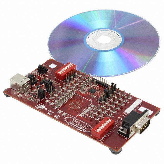
SP338EER1-0A-EB产品简介:
ICGOO电子元器件商城为您提供SP338EER1-0A-EB由Exar设计生产,在icgoo商城现货销售,并且可以通过原厂、代理商等渠道进行代购。 SP338EER1-0A-EB价格参考。ExarSP338EER1-0A-EB封装/规格:评估和演示板和套件, SP338E Transceiver, RS-232, RS-422, RS-485 Interface Evaluation Board。您可以下载SP338EER1-0A-EB参考资料、Datasheet数据手册功能说明书,资料中有SP338EER1-0A-EB 详细功能的应用电路图电压和使用方法及教程。
MaxLinear, Inc. 是一家专注于射频(RF)、混合信号集成电路和通信解决方案的半导体公司。型号为 SP338EER1-0A-EB 的产品属于其评估和演示板套件系列,主要用于评估 SP338 芯片的性能。

该评估板的主要应用场景包括:

1. 通信系统开发:SP338EER1-0A-EB 用于测试和开发基于 SP338 芯片的通信设备,该芯片通常用于高速数据传输系统,如光纤通信、无线基站和宽带接入设备。

2. 射频和光电模块设计:该评估板支持工程师在设计射频和光电模块时进行信号完整性测试、功耗评估和性能优化。

3. 研发与原型设计:工程师可以利用该评估板快速搭建原型系统,验证芯片在实际应用中的表现,缩短产品开发周期。

4. 教育与培训:高校和培训机构可使用该套件帮助学生理解高速通信芯片的工作原理和应用方法。

总之,SP338EER1-0A-EB 主要面向通信行业研发人员,用于芯片评估、系统设计验证和性能优化,适用于有线和无线通信基础设施的开发。
| 参数 | 数值 |
| 产品目录 | 编程器,开发系统嵌入式解决方案 |
| 描述 | EVAL BOARD FOR SP338EER4界面开发工具 SP338 EVAL BOARD |
| 产品分类 | |
| 品牌 | Exar Corporation |
| 产品手册 | |
| 产品图片 |
|
| 产品系列 | 模拟与数字IC开发工具,界面开发工具,Exar SP338EER1-0A-EB- |
| mouser_ship_limit | 该产品可能需要其他文件才能进口到中国。 |
| 数据手册 | http://www.exar.com/common/content/document.ashx?id=20834&languageid=1033http://www.exar.com/common/content/document.ashx?id=21297 |
| 产品型号 | SP338EER1-0A-EB |
| rohs | 无铅 / 符合限制有害物质指令(RoHS)规范要求 |
| 主要属性 | 3 驱动器,5 接收器 |
| 主要用途 | 接口,收发器,RS-232,RS-422,RS-485 |
| 产品 | Evaluation Boards |
| 产品培训模块 | http://www.digikey.cn/PTM/IndividualPTM.page?site=cn&lang=zhs&ptm=26101 |
| 产品种类 | 界面开发工具 |
| 使用的IC/零件 | SP338E |
| 其它名称 | 1016-1932 |
| 商标 | Exar |
| 嵌入式 | 否 |
| 工作电源电压 | 3.3 V to 5 V |
| 工作电源电流 | 10 mA |
| 工具用于评估 | SP338EER |
| 所含物品 | 板 |
| 接口类型 | RS-232, RS-422, RS-485 |
| 最大工作温度 | + 85 C |
| 最小工作温度 | - 40 C |
| 标准包装 | 1 |
| 类型 | RS-232, RS-422, RS-485 |
| 辅助属性 | - |


- 商务部:美国ITC正式对集成电路等产品启动337调查
- 曝三星4nm工艺存在良率问题 高通将骁龙8 Gen1或转产台积电
- 太阳诱电将投资9.5亿元在常州建新厂生产MLCC 预计2023年完工
- 英特尔发布欧洲新工厂建设计划 深化IDM 2.0 战略
- 台积电先进制程称霸业界 有大客户加持明年业绩稳了
- 达到5530亿美元!SIA预计今年全球半导体销售额将创下新高
- 英特尔拟将自动驾驶子公司Mobileye上市 估值或超500亿美元
- 三星加码芯片和SET,合并消费电子和移动部门,撤换高东真等 CEO
- 三星电子宣布重大人事变动 还合并消费电子和移动部门
- 海关总署:前11个月进口集成电路产品价值2.52万亿元 增长14.8%


PDF Datasheet 数据手册内容提取
SP338E RS-232/RS-485/RS-422 TRANSCEIVER WITH INTERNAL TERMINATION FEBRUARY 2018 REV. 1.0.1 GENERAL DESCRIPTION FEATURES The SP338 is an advanced multiprotocol transceiver Pin selectable Cable Termination supporting RS-232, RS-485, and RS-422 serial No external resistors required for RS-485/422 standards in a 40 pin QFN package. Integrated cable termination and biasing termination and four configuration modes allow all three protocols to be used interchangeably over a 3.3V or 5V Single Supply Operation single cable or connector with no additional switching Robust ESD Protection on bus pins components. Full operation requires only four external charge pump capacitors. ■ ±15kV Human Body Model (HBM) ■ ±8kV IEC 61000-4-2 (Contact) The RS-485/422 modes feature up to two drivers and four receivers (2TX/4RX) in half, full, and mixed Max Data Rate of 20Mbps in RS-485/422 Modes duplex configurations. The RS-232 mode (3TX/5RX) and up to 1Mbps in RS-232 Modes provides full support of all eight signals commonly Pin selectable 250kbps Slew Limiting used with the DB9 RS-232 connector. A dedicated diagnostic loopback mode is also provided. 3 Drivers, 5 Receivers RS-232/V.28 The high speed drivers operate up to 20Mbps in RS- 2 Drivers, 4 Receivers RS-485/422 485/422 modes, and up to 1Mbps in RS-232 mode. ■ Full, Half, and Mixed Duplex Configurations All drivers can be slew limited to 250kbps in any ■ 1/8th Unit Load, up to 256 receivers on bus mode to minimize electromagnetic interference (EMI). RS-485/422 Enhanced Failsafe for open, shorted, All transmitter outputs and receiver inputs feature or terminated but idle inputs robust electrostatic discharge (ESD) protection to ±15kV Human Body Model (HBM) and ±8kV IEC- Space saving 6mm x 6mm QFN-40 Package 61000-4-2 Contact. Each receiver output has full fail- Pin compatible with SP339E safe protection to avoid system lockup, oscillation, or indeterminate states by defaulting to logic-high output level when the inputs are open, shorted, or terminated but undriven. No external biasing resistors are required. TYPICAL APPLICATIONS The RS-232 receiver inputs include a 5k pull-down Dual Protocol Serial Ports (RS-232 or RS-485/422) to ground. The RS-485/422 receiver inputs are high Industrial Computers impedance (>96k when termination is disabled), allowing up to 256 devices on a single Industrial and Process Control Equipment communication bus (1/8th unit load). Point-Of-Sale Equipment The SP338 operates from a single power supply, Networking Equipment either 3.3V or 5V, with low idle current. The shutdown mode consumes less than 10µA for low power HVAC Controls Equipment standby operation. Building Security and Automation Equipment ORDERING INFORMATION(1) PART NUMBER OPERATING TEMPERATURE RANGE LEAD-FREE PACKAGE PACKAGING METHOD SP338EER1-L Tray -40°C to +85°C Yes(2) 40-pin QFN SP338EER1-L/TR Tape and Reel NOTE: 1. Refer to www.exar.com/SP338E for most up-to-date Ordering Information. 2. Visit www.exar.com for additional information on Environmental Rating. 1
SP338E RS-232/RS-485/RS-422 TRANSCEIVER WITH INTERNAL TERMINATION REV. 1.0.1 ABSOLUTE MAXIMUM RATINGS These are stress ratings only and functional operation of the device at these ratings or any other above those indicated in the operation sections to the specifications below is not implied. Exposure to absolute maximum rating conditions for extended periods of time may affect reliability and cause permanent damage to the device. Supply Voltage VCC -0.3V to +6.0V Receiver Input Voltage (from Ground) ±18V Driver Output Voltage (from Ground) ±18V Short Circuit Duration, TX out to Ground Continuous Voltage at TTL Input Pins -0.3V to (VCC + 0.5V) Storage Temperature Range -65°C to +150°C Lead Temperature (soldering, 10s) +300°C Power Dissipation 40-pin QFN 500mW (derate 17mW/°C above +70°C) ESD Ratings HBM - Human Body Model (Tx Output & Rx Input pins, R1-R9) ±15kV HBM - Human Body Model (All other pins) ±2kV IEC61000-4-2 Contact Discharge (Tx Output & Rx Input pins, R1-R9) ±8kV CAUTION: ESD (ElectroStatic Discharge) sensitive device. Permanent damage may occur on unconnected devices subject to high energy electrostatic fields. Unused devices must be stored in conductive foam or shunts. Personnel should be properly grounded prior to handling this device. The protective foam should be discharged to the destination socket before devices are removed. 2
SP338E REV. 1.0.1 RS-232/RS-485/RS-422 TRANSCEIVER WITH INTERNAL TERMINATION PIN DESCRIPTIONS BY MODE (MODE2, MODE1, MODE0) 000, 001, 010, 011, 100, 101, 110, 111, Pin Name Figure 1 Figure 2 Figure 3 Figure 4 Figure 5 Figure 6 Figure 7 Figure 8 1 L1 R1 Output 1 1 1 1 1 1 2 L2 R2 Output R1 Output R1 Output R1 Output R1 Output R1 Output R1 Output 3 L3 T1 Input T1 Input T1 Input T1 Input T1 Input T1 Input T1 Input 4 L4 T2 Input 5 L6 R3 Output 1 1 1 1 1 R2 Output 6 L7 T3 Input T2 Input T2 Input 7 L8 R4 Output 1 1 R2 Output 1 1 R3 Output 8 L9 R5 Output 1 1 1 1 1 R4 Output 9 VCC VCC 10 GND Ground 11 SLEW SLEW = VCC enables 250kbps slew limiting T1 Enable, T1 Enable, T1 Enable, 12 DIR1 T1 Enable T1 Enable T1 Enable R1 Disable R1 Disable R1 Disable T2 Enable, 13 DIR2 T2 Enable R2 Disable 14 MODE0 0 1 0 1 0 1 0 1 15 MODE1 0 0 1 1 0 0 1 1 16 MODE2 0 0 0 0 1 1 1 1 17 TERM Enables RS-485/422 receiver termination 18 INVDIR Inverts DIR1 and DIR2, where applicable 19 ENABLE ENABLE = VCC for operation, ENABLE = 0V for shutdown 20 VCC VCC 3
SP338E RS-232/RS-485/RS-422 TRANSCEIVER WITH INTERNAL TERMINATION REV. 1.0.1 PIN DESCRIPTIONS BY MODE (MODE2, MODE1, MODE0) 000, 001, 010, 011, 100, 101, 110, 111, Pin Name Figure 1 Figure 2 Figure 3 Figure 4 Figure 5 Figure 6 Figure 7 Figure 8 21 R9 R5 Input R2 Input B R1 Input B R4 Input B 22 R8 R4 Input R2 Input A R4 Input A 23 GND Ground R3 Input A 24 R7 T3 Output T2 Out A R1 Input A T2 Out A R3 Input B 25 R6 R3 Input T2 Out B T2 Out B 26 GND Ground R1 Input A 27 R4 T2 Output R1 Input B R1 Input B T1 Out A R2 Input B T1 Out A 28 R3 T1 Output R2 Input A R1 Input A R2 Input A 29 GND Ground R1 Input A R1 Input A 30 R2 R2 Input T1 Out A T1 Out A T1 Out A T1 Out A R1 Input B R1 Input B R1 Input B 31 R1 R1 Input T1 Out B T1 Out B T1 Out B T1 Out B T1 Out B T1 Out B 32 VCC VCC 33 VSS VSS - Charge pump negative supply, 0.1uF from ground 34 C2- C2+ - Charge pump cap 2 negative lead 35 C1- C1- - Charge pump cap 1 negative lead 36 GND Ground 37 C1+ C1+ - Charge pump cap 1 positive lead, 0.1uF 38 VCC VCC 39 C2+ C2+ - Charge pump cap 2 positive lead, 0.1uF 40 VDD VDD - Charge pump positive supply, 0.1uF to ground 4
SP338E REV. 1.0.1 RS-232/RS-485/RS-422 TRANSCEIVER WITH INTERNAL TERMINATION ELECTRICAL CHARACTERISTICS UNLESS OTHERWISE NOTED: V = +3.3V ±5% or +5.0V ±5%, C1-C4 = 0.1F; T = T to T . Typical values are at V = 3.3V, T = +25°C. CC A MIN MAX CC A SYMBOL PARAMETERS MIN. TYP. MAX. UNITS CONDITIONS DC CHARACTERISTICS ICC Supply Current (RS-232) 2 10 mA No load, idle inputs ICC Supply Current (RS-485) 4 10 mA No load, idle inputs ICC Vcc Shutdown Current 1 10 A ENABLE = 0V TRANSMITTER and LOGIC INPUT PINS: Pins 3, 4, 6, 11-19 VIH Logic Input Voltage High 2.0 V VCC = 3.3V VIH Logic Input Voltage High 2.4 V VCC = 5.0V VIL Logic Input Voltage Low 0.8 V IIL Logic Input Leakage Current Low 1 A Input Low (VIN = 0V) Input High (V = V ), IIH Logic Input Leakage Current High 1 A IN CC pins 3, 4 and 6 Input High (V = V ), IPD Logic Input Pull-down Current 50 A IN CC pins 11-19 VHYS Logic Input Hysteresis 200 mV RECEIVER OUTPUTS: Pins 1, 2, 5, 7, 8 VOH Receiver Output Voltage High VCC-0.6 V IOUT = -1.5mA VOL Receiver Output Voltage Low 0.4 V IOUT = 2.5mA IOSS Receiver Output ShortCircuit Current ±20 ±60 mA 0 VO VCC 0 V V IOZ Receiver Output Leakage Current ±0.1 ±1 A O CC, Receivers disabled 5
SP338E RS-232/RS-485/RS-422 TRANSCEIVER WITH INTERNAL TERMINATION REV. 1.0.1 ELECTRICAL CHARACTERISTICS (Continued) UNLESS OTHERWISE NOTED: V = +3.3V ±5% or +5.0V ±5%, C1-C4 = 0.1F; T = T to T . Typical values are at V = 3.3V, T = +25°C. CC A MIN MAX CC A SYMBOL PARAMETERS MIN. TYP. MAX. UNITS CONDITIONS SINGLE-ENDED RECEIVER INPUTS (RS-232) VIN Input Voltage Range -15 +15 V 0.6 1.2 V VCC = 3.3V VIL Input Threshold Low 0.8 1.5 V VCC = 5.0V 1.5 2.0 V VCC = 3.3V VIH Input Threshold High 1.8 2.4 V VCC = 5.0V VHYS Input Hysteresis 0.3 V RIN Input Resistance 3 5 7 k -15V VIN +15V SINGLE-ENDED DRIVER OUTPUTS (RS-232) ±5.0 ±5.5 V Output loaded with 3kto Gnd VO Output Voltage Swing ±7.0 V No load output ISC Short Circuit Current ±60 mA VO = 0V ROFF Power Off Impedance 300 10M VCC = 0V, VO = ±2V 6
SP338E REV. 1.0.1 RS-232/RS-485/RS-422 TRANSCEIVER WITH INTERNAL TERMINATION ELECTRICAL CHARACTERISTICS (Continued) UNLESS OTHERWISE NOTED: V = +3.3V ±5% or +5.0V ±5%, C1-C4 = 0.1F; T = T to T . Typical values are at V = 3.3V, T = +25°C. CC A MIN MAX CC A SYMBOL PARAMETERS MIN. TYP. MAX. UNITS CONDITIONS DIFFERENTIAL RECEIVER INPUTS (RS-485 / RS-422) TERM = 0V, RIN Receiver Input Resistance 96 k -7V V +12V IN Receiver Differential Threshold VTH -200 -125 -50 mV Voltage VTH Receiver Input Hysteresis 25 mV VCM = 0V 125 A VIN = +12V IIN Receiver Input Current -100 A VIN = -7V TERM = V , Figure 9 CC RTERM Termination Resistance 100 120 155 -7V V +12V CM TERM = V , Figure 9 CC RTERM Termination Resistance 100 120 140 V = 0V CM DIFFERENTIAL DRIVER OUTPUTS (RS-485 / RS-422) 2 VCC V RL = 100 (RS-422), Figure 10 1.5 VCC V RL = 54 (RS-485), Figure 10 VOD Differential Driver Output 1.5 VCC V VCM = -7V, Figure 11 1.5 VCC V VCM = +12V, Figure 11 Change In Magnitude of VOD -0.2 +0.2 V RL = 54 or 100, Figure 10 Differential Output Voltage VCM Driver CommonMode Output Voltage 3 V RL = 54 or 100, Figure 10 Change In Magnitude of VCM 0.2 V RL = 54 or 100, Figure 10 Common Mode Output Voltage IOSD Driver Output Short Circuit Current ±250 mA -7V VO +12V, Figure 12 ENABLE = 0V, or DIR1 = 0V and DIR2 = 0V in IO Driver Output Leakage Current ±100 A full duplex modes, -7V V +12V O 7
SP338E RS-232/RS-485/RS-422 TRANSCEIVER WITH INTERNAL TERMINATION REV. 1.0.1 TIMING CHARACTERISTICS UNLESS OTHERWISE NOTED: V = +3.3V ±5% or +5.0V ±5%, C1-C4 = 0.1F; T = T to T . Typical values are at V = 3.3V, T = +25°C. CC A MIN MAX CC A SYMBOL PARAMETERS MIN. TYP. MAX. UNITS CONDITIONS ALL MODES tENABLE Enable from Shutdown 1000 ns tSHUTDOWN Enable to Shutdown 1000 ns RS-232, DATA RATE = 250kbps (SLEW = Vcc), ONE TRANSMITTER SWITCHING Maximum Data Rate 250 kbps RL = 3k, CL = 1000pF tRHL, tRLH Receiver Propagation Delay 100 ns C = 150pF, Figure 13 L tRHL-tRLH Receiver Propagation Delay Skew 100 ns tDHL, tDLH Driver Propagation Delay 1400 ns RL = 3k, CL = 2500pF, tDHL-tDLH Driver Propagation Delay Skew 600 ns Figure 14 V = 3.3V, R = 3k to 7k CC L Transition Region Slew Rate from tSHL, tSLH +3.0V to -3.0V or -3.0V to +3.0V 4 30 V/s CL = 150pF to 2500pF, Figure 14 V = 3.3V, R = 3k to 7k CC L Transition Region Slew Rate from tSHL, tSLH +3.0V to -3.0V or -3.0V to +3.0V 6 30 V/s CL = 150pF to 2500pF, T = 25°C, Figure 14 A RS-232, DATA RATE = 1Mbps (SLEW = 0V), ONE TRANSMITTER SWITCHING Maximum Data Rate 1 Mbps RL = 3k, CL = 250pF tRHL, tRLH Receiver Propagation Delay 100 ns C = 150pF, Figure 13 L tRHL-tRLH Receiver Propagation Delay Skew 100 ns tDHL, tDLH Driver Propagation Delay 300 ns RL = 3k, CL = 1000pF, tDHL-tDLH Driver Propagation Delay Skew 150 ns Figure 14 V = 3.3V, R = 3k to 7k CC L Transition Region Slew Rate from tSHL, tSLH +3.0V to -3.0V or -3.0V to +3.0V 15 150 V/s CL = 150pF to 1000pF, Figure 14 V = 3.3V, R = 3k to 7k CC L Transition Region Slew Rate from tSHL, tSLH +3.0V to -3.0V or -3.0V to +3.0V 24 150 V/s CL = 150pF to 1000pF, T = 25°C, Figure 14 A 8
SP338E REV. 1.0.1 RS-232/RS-485/RS-422 TRANSCEIVER WITH INTERNAL TERMINATION TIMING CHARACTERISTICS (Continued) UNLESS OTHERWISE NOTED: V = +3.3V ±5% or +5.0V ±5%, C1-C4 = 0.1F; T = T to T . Typical values are at V = 3.3V, T = +25°C. CC A MIN MAX CC A SYMBOL PARAMETERS MIN. TYP. MAX. UNITS CONDITIONS RS-485/RS-422, DATA RATE = 250kbps (SLEW = Vcc), ONE TRANSMITTER SWITCHING Maximum Data Rate 250 kbps R = 54C = 50pF L L tRPHL, tRPLH Receiver Propagation Delay 50 150 ns C = 15pF, Figure 15 L tRPHL-tRPLH Receiver Propagation Delay Skew 20 ns tDPHL, tDPLH Driver Propagation Delay 500 1000 ns R = 54C = 50pF, tDPHL-tDPLH Driver Propagation Delay Skew 100 ns L L Figure 16 tDR, tDF Driver Rise and Fall Time 300 650 1200 ns tRZH, tRZL Receiver Output Enable Time 200 ns C = 15pF, Figure 17 L tRHZ, tRLZ Receiver Output Disable Time 200 ns tDZH, tDZL Driver Output Enable Time 1000 ns RL = 500CL = 50pF, tDHZ, tDLZ Driver Output Disable Time 200 ns Figure 18 RS-485/RS-422, DATA RATE = 20Mbps (SLEW = 0V), ONE TRANSMITTER SWITCHING Maximum Data Rate 20 Mbps RL = 54CL = 50pF tRPHL, tRPLH Receiver Propagation Delay 50 150 ns C = 15pF, Figure 15 L tRPHL-tRPLH Receiver Propagation Delay Skew 10 ns tDPHL, tDPLH Driver Propagation Delay 30 100 ns R = 54C = 50pF, tDPHL-tDPLH Driver Propagation Delay Skew 10 ns L L Figure 16 tDR, tDF Driver Rise and Fall Time 10 20 ns tRZH, tRZL Receiver Output Enable Time 200 ns C = 15pF, Figure 17 L tRHZ, tRLZ Receiver Output Disable Time 200 ns tDZH, tDZL Driver Output Enable Time 200 ns RL = 500CL = 50pF, tDHZ, tDLZ Driver Output Disable Time 200 ns Figure 18 9
SP338E RS-232/RS-485/RS-422 TRANSCEIVER WITH INTERNAL TERMINATION REV. 1.0.1 BLOCK DIAGRAM BY MODE (MODE2, MODE1, MODE0) FIGURE 1. MODE 000 - LOOPBACK 10
SP338E REV. 1.0.1 RS-232/RS-485/RS-422 TRANSCEIVER WITH INTERNAL TERMINATION FIGURE 2. MODE 001 - RS-232 11
SP338E RS-232/RS-485/RS-422 TRANSCEIVER WITH INTERNAL TERMINATION REV. 1.0.1 FIGURE 3. MODE 010 - RS-485 HALF DUPLEX #1 12
SP338E REV. 1.0.1 RS-232/RS-485/RS-422 TRANSCEIVER WITH INTERNAL TERMINATION FIGURE 4. MODE 011 - RS-485/422 FULL DUPLEX #1 13
SP338E RS-232/RS-485/RS-422 TRANSCEIVER WITH INTERNAL TERMINATION REV. 1.0.1 FIGURE 5. MODE 100 - RS-485/422 FULL DUPLEX #2 14
SP338E REV. 1.0.1 RS-232/RS-485/RS-422 TRANSCEIVER WITH INTERNAL TERMINATION FIGURE 6. MODE 101 - RS-485/422 FULL DUPLEX #3 15
SP338E RS-232/RS-485/RS-422 TRANSCEIVER WITH INTERNAL TERMINATION REV. 1.0.1 FIGURE 7. MODE 110 - RS-485 HALF DUPLEX #2 16
SP338E REV. 1.0.1 RS-232/RS-485/RS-422 TRANSCEIVER WITH INTERNAL TERMINATION FIGURE 8. MODE 111 - RS-485/422 MIXED DUPLEX 17
SP338E RS-232/RS-485/RS-422 TRANSCEIVER WITH INTERNAL TERMINATION REV. 1.0.1 TEST FIXTURES FIGURE 9. RS-485/422 RECEIVER TERMINATION RESISTANCE FIGURE 10. RS-485/422 DIFFERENTIAL DRIVER OUTPUT VOLTAGE FIGURE 11. RS-485/422 DIFFERENTIAL DRIVER OUTPUT VOLTAGE OVER COMMON MODE 18
SP338E REV. 1.0.1 RS-232/RS-485/RS-422 TRANSCEIVER WITH INTERNAL TERMINATION FIGURE 12. RS-485/422 DRIVER OUTPUT SHORT CIRCUIT CURRENT FIGURE 13. RS-232 RECEIVER PROPAGATION DELAY 19
SP338E RS-232/RS-485/RS-422 TRANSCEIVER WITH INTERNAL TERMINATION REV. 1.0.1 FIGURE 14. RS-232 DRIVER PROPAGATION DELAY FIGURE 15. RS-485/422 RECEIVER PROPAGATION DELAY 20
SP338E REV. 1.0.1 RS-232/RS-485/RS-422 TRANSCEIVER WITH INTERNAL TERMINATION FIGURE 16. RS-485/422 DRIVER PROPAGATION DELAY AND RISE/FALL TIMES FIGURE 17. RS-485/422 RECEIVER OUTPUT ENABLE/DISABLE TIMES 21
SP338E RS-232/RS-485/RS-422 TRANSCEIVER WITH INTERNAL TERMINATION REV. 1.0.1 FIGURE 18. RS-485/422 DRIVER OUTPUT ENABLE/DISABLE TIMES 22
SP338E REV. 1.0.1 RS-232/RS-485/RS-422 TRANSCEIVER WITH INTERNAL TERMINATION PRODUCT SUMMARY The SP338 is an advanced multiprotocol transceiver supporting RS-232, RS-485, and RS-422 serial standards in a 40 pin QFN package. Integrated cable termination and four configuration modes allow all three protocols to be used interchangeably over a single cable or connector with no additional switching components. The RS- 485/422 modes feature up to two drivers and four receivers (2TX/4RX) in half, full, and mixed duplex configurations. The RS-232 mode (3TX/5RX) provides full support of all eight signals commonly used with the DB9 RS-232 connector. A dedicated mode is also available for diagnostic loopback testing. INTERNALLY SWITCHED CABLE TERMINATION Enabling and disabling the RS-485/422 termination resistor is one of the largest challenges system designers face when sharing a single connector or pair of lines between multiple serial protocols. A termination resistor may be necessary for accurate RS-485/422 communication, but must be removed when the lines are used for RS-232. SP338 provides an elegant solution to this problem by integrating the termination resistor and switching control, and allowing it to be switched in and out of the circuit with a single pin. No external switching components are required. ENHANCED FAILSAFE Ordinary RS-485 differential receivers will be in an indeterminate state whenever the data bus is not being actively driven. The enhanced failsafe feature of the SP338 guarantees a logic-high receiver output when the receiver inputs are open, shorted, or terminated but idle/undriven. The enhanced failsafe interprets 0V differential as a logic high with a minimum 50mV noise margin, while maintaining compliance with the EIA/TIA- 485 standard of ±200mV. No external biasing resistors are required, further easing the usage of multiple protocols over a single connector. ±15kV ESD PROTECTION ESD protection structures are incorporated on all pins to protect against electrostatic discharges encountered during handling and assembly. The bus pins (driver outputs and receiver inputs) have extra protection structures, which have been tested up to ±15kV without damage. These structures withstand high ESD in all states: normal operation, shutdown and powered down. ESD protection is be tested in various ways. Maxlinear uses the following methods to qualify the protection structures designed into SP338: ±15kV using the Human Body Model (HBM) ±-8kV using IEC 61000-4-2 Contact Discharge The IEC 61000-4-2 standard is more rigorous than HBM, resulting in lower voltage levels compared with HBM for the same level of ESD protection. Because IEC 61000-4-2 specifies a lower series resistance, the peak current is higher than HBM. The SP338 has passed both HBM and IEC 61000-4-2 testing without damage. DIAGNOSTIC LOOPBACK MODE The SP338 includes a diagnostic digital loop back mode for system testing as shown in Figure 1. The loopback mode connects the TTL driver inputs to the TTL receiver outputs, bypassing the analog driver and receiver circuitry. The analog/bus pins are internally disconnected in this mode. 23
SP338E RS-232/RS-485/RS-422 TRANSCEIVER WITH INTERNAL TERMINATION REV. 1.0.1 MECHANICAL DIMENSIONS FIGURE 19. QFN40 TOP VIEW BOTTOM VIEW SIDE VIEW TERMINAL DETAILS Drawing No.: POD-00000041 Revision: B.1 24
SP338E REV. 1.0.1 RS-232/RS-485/RS-422 TRANSCEIVER WITH INTERNAL TERMINATION RECOMMENDED LAND PATTERN AND STENCILS FIGURE 20. QFN40 TYPICAL RECOMMEDED LAND PATTERN TYPICAL RECOMMEDED STENCIL Drawing No.: POD-00000041 Revision: B.1 25
SP338E RS-232/RS-485/RS-422 TRANSCEIVER WITH INTERNAL TERMINATION REV. 1.0.1 REVISION HISTORY DATE REVISION DESCRIPTION November 2011 1.0.0 Production Release February 2018 1.0.1 Update to MaxLinear logo. Update format and Ordering Information. Moved ESD ratings on page 2. Corporate Headquarters: High Performance Analog: 5966 LaPlace Court 1060 Rincon Circle Suite 100 San Jose, CA 95131 Carlsbad, CA 92008 Tel.:+1 (669) 265-6100 Tel.:+1 (760) 692-0711 Fax: +1 (669) 265-6101 Fax:+1 (760) 444-8598 Email: serialtechsupport@exar.com www.maxlinear.com www.exar.com The content of this document is furnished for informational use only, is subject to change without notice, and should not be construed as a commitment by MaxLinear, Inc.. MaxLinear, Inc. assumes no responsibility or liability for any errors or inaccuracies that may appear in the informational content contained in this guide. Complying with all applicable copyright laws is the responsibility of the user. Without limiting the rights under copyright, no part of this document may be reproduced into, stored in, or introduced into a retrieval system, or transmitted in any form or by any means (electronic, mechanical, photocopying, recording, or otherwise), or for any purpose, without the express written permission of MaxLinear, Inc. Maxlinear, Inc. does not recommend the use of any of its products in life support applications where the failure or malfunction of the product can reasonably be expected to cause failure of the life support system or to significantly affect its safety or effectiveness. Products are not authorized for use in such applications unless MaxLinear, Inc. receives, in writing, assur- ances to its satisfaction that: (a) the risk of injury or damage has been minimized; (b) the user assumes all such risks; (c) potential liability of MaxLinear, Inc. is adequately protected under the circumstances. MaxLinear, Inc. may have patents, patent applications, trademarks, copyrights, or other intellectual property rights covering subject matter in this document. Except as expressly provided in any written license agreement from MaxLinear, Inc., the furnishing of this document does not give you any license to these patents, trademarks, copyrights, or other intellectual property. Company and product names may be registered trademarks or trademarks of the respective owners with which they are associated. © 2011 - 2018 MaxLinear, Inc. All rights reserved 26
Mouser Electronics Authorized Distributor Click to View Pricing, Inventory, Delivery & Lifecycle Information: E xar: SP338ECR1-L SP338ECR1-L/TR SP338EER1-0A-EB SP338EER1-L SP338EER1-L/TR