ICGOO在线商城 > 集成电路(IC) > PMIC - 栅极驱动器 > IRS2186SPBF
/IRS2186SPBF.jpg)
 Datasheet下载
- 型号: IRS2186SPBF
- 制造商: International Rectifier
- 库位|库存: xxxx|xxxx
- 要求:
| 数量阶梯 | 香港交货 | 国内含税 |
| +xxxx | $xxxx | ¥xxxx |
查看当月历史价格
查看今年历史价格
IRS2186SPBF产品简介:
ICGOO电子元器件商城为您提供IRS2186SPBF由International Rectifier设计生产,在icgoo商城现货销售,并且可以通过原厂、代理商等渠道进行代购。 IRS2186SPBF价格参考。International RectifierIRS2186SPBF封装/规格:PMIC - 栅极驱动器, Half-Bridge Gate Driver IC Non-Inverting 8-SOIC。您可以下载IRS2186SPBF参考资料、Datasheet数据手册功能说明书,资料中有IRS2186SPBF 详细功能的应用电路图电压和使用方法及教程。
IRS2186SPBF是英飞凌(Infineon Technologies)推出的PMIC(电源管理集成电路)系列中的一个栅极驱动器型号。该器件主要用于驱动MOSFET或IGBT等功率开关元件,广泛应用于各种需要高效功率转换和控制的场景。以下是其主要应用场景:

 1. 电机驱动
   - IRS2186SPBF常用于无刷直流电机(BLDC)和永磁同步电机(PMSM)的驱动电路中。它能够提供高侧和低侧栅极驱动信号,支持半桥或全桥拓扑结构,适用于家电(如空调、冰箱、洗衣机)、电动工具和工业自动化设备中的电机控制。

 2. 开关电源(SMPS)
   - 在开关电源设计中,该芯片可用于驱动功率MOSFET或IGBT,实现高效的DC-DC或AC-DC转换。其高速驱动能力和良好的抗噪性能使其适合于适配器、充电器以及工业电源等应用。

 3. 太阳能逆变器
   - 在光伏系统中,IRS2186SPBF可用于驱动逆变器中的功率开关,将直流电转换为交流电。其高效驱动特性有助于提高能量转换效率,降低系统损耗。

 4. 电动车与混合动力车(EV/HEV)
   - 在电动车和混合动力车中,该芯片可应用于电池管理系统(BMS)、车载充电器(OBC)和电机控制器中,用于驱动功率器件以实现能量管理和动力输出。

 5. 不间断电源(UPS)
   - IRS2186SPBF在UPS系统中用于驱动功率开关,确保在市电中断时能够快速切换到备用电源,并稳定输出电压。

 6. 照明系统
   - 在LED照明领域,尤其是大功率LED驱动器中,该芯片可用于驱动功率级电路,提供稳定的电流输出,同时支持调光功能。

 特性总结:
IRS2186SPBF具有以下关键特性,使其适用于上述场景:
- 支持高达600V的电源电压。
- 高侧和低侧驱动通道之间的死区时间可调,防止直通。
- 内置欠压锁定保护(UVLO),增强系统可靠性。
- 高速驱动能力,降低开关损耗。
- 良好的电磁兼容性(EMC)性能,适合复杂电磁环境下的应用。

总之,IRS2186SPBF是一款高性能的栅极驱动器,适用于多种需要高效功率转换和精确控制的应用场合。
| 参数 | 数值 |
| 产品目录 | 集成电路 (IC)半导体 |
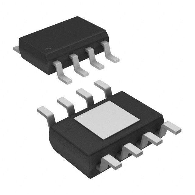
| 描述 | IC DRIVER HI/LO SIDE 600V 8-SOIC门驱动器 3-Phase Bridge DRVR 600V 10V to 20V |
| 产品分类 | PMIC - MOSFET,电桥驱动器 - 外部开关集成电路 - IC |
| 品牌 | International Rectifier |
| 产品手册 | |
| 产品图片 |
|
| rohs | 符合RoHS无铅 / 符合限制有害物质指令(RoHS)规范要求 |
| 产品系列 | 电源管理 IC,门驱动器,International Rectifier IRS2186SPbF- |
| 数据手册 | |
| 产品型号 | IRS2186SPBF |
| 上升时间 | 38 ns |
| 下降时间 | 30 ns |
| 产品 | Half-Bridge Drivers |
| 产品培训模块 | http://www.digikey.cn/PTM/IndividualPTM.page?site=cn&lang=zhs&ptm=26250 |
| 产品种类 | 门驱动器 |
| 供应商器件封装 | 8-SOIC |
| 包装 | 管件 |
| 商标 | International Rectifier |
| 安装类型 | 表面贴装 |
| 安装风格 | SMD/SMT |
| 封装 | Tube |
| 封装/外壳 | 8-SOIC(0.154",3.90mm 宽) |
| 封装/箱体 | SOIC-8 |
| 工作温度 | -40°C ~ 125°C |
| 工厂包装数量 | 95 |
| 延迟时间 | 170ns |
| 最大关闭延迟时间 | 170 ns |
| 最大功率耗散 | 625 mW |
| 最大工作温度 | + 125 C |
| 最大开启延迟时间 | 170 ns |
| 最小工作温度 | - 40 C |
| 标准包装 | 95 |
| 激励器数量 | 2 Driver |
| 电压-电源 | 10 V ~ 20 V |
| 电流-峰值 | 4A |
| 电源电压-最大 | 20 V |
| 电源电压-最小 | 10 V |
| 电源电流 | 0.24 mA |
| 类型 | High Side/Low Side |
| 输入类型 | 非反相 |
| 输出数 | 2 |
| 输出电压 | 10 V to 20 V |
| 输出电流 | 4 A |
| 输出端数量 | 2 |
| 配置 | 高端和低端,独立 |
| 配置数 | 1 |
| 高压侧电压-最大值(自举) | 600V |


- 商务部:美国ITC正式对集成电路等产品启动337调查
- 曝三星4nm工艺存在良率问题 高通将骁龙8 Gen1或转产台积电
- 太阳诱电将投资9.5亿元在常州建新厂生产MLCC 预计2023年完工
- 英特尔发布欧洲新工厂建设计划 深化IDM 2.0 战略
- 台积电先进制程称霸业界 有大客户加持明年业绩稳了
- 达到5530亿美元!SIA预计今年全球半导体销售额将创下新高
- 英特尔拟将自动驾驶子公司Mobileye上市 估值或超500亿美元
- 三星加码芯片和SET,合并消费电子和移动部门,撤换高东真等 CEO
- 三星电子宣布重大人事变动 还合并消费电子和移动部门
- 海关总署:前11个月进口集成电路产品价值2.52万亿元 增长14.8%


PDF Datasheet 数据手册内容提取
IRS2186(4)(S)PBF High and Low Side Driver Features Product Summary Floating channel designed for bootstrap operation V 600 V Fully operational to +600 V OFFSET Tolerant to negative transient voltage dV/dt immune IO+/- 4 A / 4 A Gate drive supply range from 10 V to 20 V Undervoltage lockout for both channels V 10 V – 20 V OUT 3.3 V and 5 V logic compatible Matched propagation delay for both channels Ton/off (typ.) 170 & 170 ns Logic and power ground +/- 5 V offset Lower di/dt gate driver for better noise immunity Output source/sink current 4 A / 4 A RoHS compliant Package Options Description The IRS2186(4) are high voltage, high speed power MOSFET and IGBT drivers with independent high-side and low-side referenced output channels. Proprietary HVIC and latch immune CMOS technologies enable ruggedized monolithic construction. The logic input is compatible with standard CMOS or LSTTL output, down to 3.3 V logic. The output drivers feature a high pulse current buffer stage designed for minimum driver cross-conduction. The floating 8-Lead SOIC 8-Lead PDIP channel can be used to drive an N-channel power MOSFET or IGBT in the high-side configuration which operates up to 600 V. 14-Lead SOIC 14-Lead PDIP Ordering Information Standard Pack Base Part Number Package Type Orderable Part Number Form Quantity IRS2186SPBF SO8N Tube 95 IRS2186SPBF IRS2186SPBF SO8N Tape and Reel 2500 IRS2186STRPBF IRS21864SPBF SO14N Tube 55 IRS21864SPBF IRS21864SPBF SO14N Tape and Reel 2500 IRS21864STRPBF IRS2186PBF PDIP8 Tube 50 IRS2186PBF IRS21864PBF PDIP14 Tube 25 IRS21864PBF 1 www.irf.com © 2015 International Rectifier April 30, 2015
IRS2186(4)(S)PBF Table of Contents Page Description 1 Ordering Information 1 Typical Connection Diagram 3 Absolute Maximum Ratings 4 Recommended Operating Conditions 4 Dynamic Electrical Characteristics 5 Static Electrical Characteristics 5 Functional Block Diagrams 6 Lead Definitions 7 Lead Assignments 7 Application Information and Additional Details 8 Package Details: PDIP8, SO8N 21 Package Details: PDIP14, SO14N 22 Tape and Reel Details: SO8N 23 Tape and Reel Details: SO14N 24 Part Marking Information 25 Qualification Information 27 2 www.irf.com © 2015 International Rectifier April 30, 2015
IRS2186(4)(S)PBF Typical Connection Diagram Up to 600V V V V CC CC B HIN HIN HO LIN LIN V S TO LOAD COM LO IRS2186(S) Up to 600V HO V V V CC CC B HIN HIN V S LIN LIN TO LOAD V V COM SS SS LO IRS21864(S) (Refer to Lead Assignments for correct pin configuration). These diagrams show electrical connections only. Please refer to our Application Notes and Design Tips for proper circuit board layout. 3 www.irf.com © 2015 International Rectifier April 30, 2015
IRS2186(4)(S)PBF Absolute Maximum Ratings Absolute maximum ratings indicate sustained limits beyond which damage to the device may occur. All voltage parameters are absolute voltages referenced to COM. The thermal resistance and power dissipation ratings are measured under board mounted and still air conditions. Symbol Definition Min. Max. Units V High side floating absolute voltage -0.3 620 † B VS High side floating supply offset voltage VB - 20 VB + 0.3 V High side floating output voltage V - 0.3 V + 0.3 HO S B V Low side and logic fixed supply voltage -0.3 20 † V CC VLO Low side output voltage -0.3 VCC + 0.3 V Logic input voltage (HIN & LIN) V - 0.3 V + 0.3 IN SS CC V Logic ground (IRS21864) V - 20 V + 0.3 SS CC CC dVS/dt Allowable offset supply voltage transient — 50 V/ns 8 lead PDIP — 1 Package power dissipation 8 lead SOIC — 0.625 P W D @ TA ≤ +25°C 14 lead PDIP — 1.6 14 lead SOIC — 1 8 lead PDIP — 125 Thermal resistance, junction to 8 lead SOIC — 200 °C/W Rth JA ambient 14 lead PDIP — 75 14 lead SOIC — 120 T Junction temperature — 150 J T Storage temperature -50 150 °C S T Lead temperature (soldering, 10 seconds) — 300 L Recommended Operating Conditions The input/output logic timing diagram is shown in figure 1. For proper operation the device should be used within the recommended conditions. The V and V offset rating is tested with all supplies biased at 15 V differential. S SS Symbol Definition Min. Max. Units V High side floating absolute voltage V + 10 V + 20 B S S VS High side floating supply offset voltage †† 600 VHO High side floating output voltage VS VB VCC Low side and logic fixed supply voltage 10 20 V V Low side output voltage 0 V LO CC V Logic input voltage (HIN & LIN) V V IN SS CC V Logic ground (IRS21864) -5 5 SS T Ambient temperature -40 125 °C A † All supplies are fully tested at 25 V and an internal 20 V clamp exists for each supply †† Logic operational for V of -5 V to 600 V. Logic state held for V of -5 V to –V (Please refer to the Design Tip DT97-3 S S BS for more details) 4 www.irf.com © 2015 International Rectifier April 30, 2015
IRS2186(4)(S)PBF Dynamic Electrical Characteristics V (V , V ) = 15 V, V = COM, C = 1000 pF and T = 25 °C unless otherwise specified. BIAS CC BS SS L A Symbol Definition Min. Typ. Max. Units Test Conditions t Turn-on propagation delay — 170 250 V = 0 V on S t Turn-off propagation delay — 170 250 V = 0 V or 600 V off S t Turn-on rise time — 22 38 ns r V = 0 V S t Turn-off fall time — 18 30 f MT Delay matching, HS & LS turn on/off — 0 35 Static Electrical Characteristics V (V , V ) = 15 V, V = COM, and T = 25 °C unless otherwise specified. The V , V and I BIAS CC BS SS A IL IH, IN parameters are referenced to V /COM and are applicable to the respective input leads HIN and LIN. The V , I SS O O, and R parameters are referenced to COM and are applicable to the respective output leads: HO and LO. ON Symbol Definition Min. Typ. Max. Units Test Conditions V Logic “1” input voltage 2.5 — — IH V = 10 V to 20 V CC V Logic “0” input voltage — — 0.8 IL V V High level output voltage, V - V — — 1.4 I = 0 A OH BIAS O O V Low level output voltage, V — — 0.15 I = 20 mA OL O O I Offset supply leakage current — — 50 V = V = 600 V LK B S I Quiescent V supply current 20 60 150 QBS BS V = 0 V or 5 V IN I Quiescent V supply current 50 120 240 μA QCC CC I Logic “1” input bias current — 25 60 V = 5 V IN+ IN I Logic “0” input bias current — — 5 V = 0 V IN- IN VCCUV+ VCC and VBS supply undervoltage 8 8.9 9.8 V positive going threshold BSUV+ VCCUV- VCC and VBS supply undervoltage 7.4 8.2 9 V V negative going threshold BSUV- V CCUVH Hysteresis 0.3 0.7 — V BSUVH Output high short circuit pulsed V = 0 V, I 2 4 — O O+ current PW ≤ 10 μs A Output low short circuit pulsed V = 15 V, I 2 4 — O O- current PW ≤ 10 μs 5 www.irf.com © 2015 International Rectifier April 30, 2015
IRS2186(4)(S)PBF Functional Block Diagram V B UV IRS2186(S) DETECT R Q HO R HV LEVEL PULSE SHIFTER FILTER S Q VSS/COM HIN LEVEL PULSE SHIFT GENERATOR VS V CC UV DETECT LO VSS/COM LIN LEVEL DELAY SHIFT COM V B UV IRS21864(S) DETECT R Q HO R HV LEVEL PULSE SHIFTER FILTER S Q VSS/COM HIN LEVEL PULSE SHIFT GENERATOR VS V CC UV DETECT LO VSS/COM LIN LEVEL DELAY SHIFT COM V SS 6 www.irf.com © 2015 International Rectifier April 30, 2015
IRS2186(4)(S)PBF Lead Definitions Symbol Description HIN Logic input for high side gate driver output (HO), in phase LIN Logic input for low side gate driver output (LO), in phase VSS Logic ground (IRS21864) V High side floating supply B HO High side gate drive output V High side floating supply return S V Low side and logic fixed supply CC LO Low side gate drive output COM Low side return Lead Assignments 1 HIN V 8 B I R 2 LIN S HO 7 2 1 3 COM 8 VS 6 6 ( 4 LO S VCC 5 ) 8-Lead SOIC / 8-Lead PDIP 1 HIN 14 2 LIN V 13 B I R 3 V S HO 12 SS 2 1 4 8 VS 11 6 4 5 COM ( 10 S ) 6 LO 9 7 V 8 CC 14-Lead SOIC / 14-Lead PDIP 7 www.irf.com © 2015 International Rectifier April 30, 2015
IRS2186(4)(S)PBF Application Information and Additional Details 50% 50% HIN HIN LIN LIN ton tr toff tf 90% 90% HO LO LO HO 10% 10% Figure 1. Input/Output Timing Diagram Figure 2. Switching Time Waveform Definitions 50% 50% HIN LIN LO HO 10% MT MT 90% LO HO Figure 3. Delay Matching Waveform Definitions 8 www.irf.com © 2015 International Rectifier April 30, 2015
IRS2186(4)(S)PBF Figure 4A. Turn-On Propagation Delay vs. Figure 4B. Turn-on Propagation Delay vs. Supply Temperature Voltage Figure 5A. Turn-Off Propagation Delay vs. Figure 5B. Turn-Off Propagation Delay vs. Supply Temperature Voltage 9 www.irf.com © 2015 International Rectifier April 30, 2015
IRS2186(4)(S)PBF 6A. Turn-On Rise Time vs. Temperature Figure 6B. Turn-On Rise Time vs. Supply Voltage Figure 7A. Turn-Off Fall Time vs. Temperature Figure 7B. Turn-Off Fall Time vs. Supply Voltage 10 www.irf.com © 2015 International Rectifier April 30, 2015
IRS2186(4)(S)PBF Figure 8B. Logic “1” Input Voltage vs. Supply Figure 8A. Logic “1” Input Voltage vs. Temperature Voltage Figure 9B. Logic “0” Input Voltage vs. Supply Figure 9A. Logic “0” Input Voltage vs. Temperature Voltage 11 www.irf.com © 2015 International Rectifier April 30, 2015
IRS2186(4)(S)PBF Figure 10A. High Level Output Voltage vs. Figure 10B. High Level Output Voltage vs. Supply Temperature (Io = 0mA) Voltage (Io = 0mA) Figure 11A. Low Level Output vs. Temperature Figure 11B. Low Level Output vs. Supply Voltage 12 www.irf.com © 2015 International Rectifier April 30, 2015
IRS2186(4)(S)PBF Figure 12B. Offset Supply Leakage Current vs. V Figure 12A. Offset Supply Leakage Current B Boost Voltage Figure 13B. V Supply Current vs. V Floating Figure 13A. V Supply Current vs. Temperature BS BS BS Supply Voltage 13 www.irf.com © 2015 International Rectifier April 30, 2015
IRS2186(4)(S)PBF Figure 14A. V Supply Current vs. Temperature Figure 14B. V Supply Current vs. Supply Voltage CC CC Figure 15A. Logic “1” Input Bias Current vs. Figure 15B. Logic “1” Input Bias Current vs. Temperature Supply Voltage 14 www.irf.com © 2015 International Rectifier April 30, 2015
IRS2186(4)(S)PBF Figure 16A. Logic “0” Input Bias Current vs. Figure 16B. Logic “0” Input Bias Current vs. Temperature Voltage Figure 17. V and V Undervoltage Threshold (+) Figure 18. V and V Undervoltage Threshold (-) CC BS CC BS vs. Temperature vs. Temperature 15 www.irf.com © 2015 International Rectifier April 30, 2015
IRS2186(4)(S)PBF Figure 19B. Output Source Current vs. Supply Figure 19A. Output Source Current vs. Temperature Voltage Figure 10B. Output Sink Current vs. Supply Figure 20A. Output Sink Current vs. Temperature Voltage 16 www.irf.com © 2015 International Rectifier April 30, 2015
IRS2186(4)(S)PBF Figure 21. IRS2186 vs. Frequency (IRFBC20) Figure 22. IRS2186 vs. Frequency (IRFBC30) R = 33Ω, V = 15V R = 22Ω, V = 15V gate CC gate CC Figure 23. IRS2186 vs. Frequency (IRFBC40) Figure 24. IRS2186 vs. Frequency (IRFPE50) R = 15Ω, V = 15V R = 10Ω, V = 15V gate CC gate CC 17 www.irf.com © 2015 International Rectifier April 30, 2015
IRS2186(4)(S)PBF Figure 25. IRS21864 vs. Frequency (IRFBC20) Figure 26. IRS21864 vs. Frequency (IRFBC30) R = 33Ω, V = 15V R = 22Ω, V = 15V gate CC gate CC Figure 27. IRS21864 vs. Frequency (IRFBC40) Figure 28. IRS21864 vs. Frequency (IRFPE50) R = 15Ω, V = 15V R = 10Ω, V = 15V gate CC gate CC 18 www.irf.com © 2015 International Rectifier April 30, 2015
IRS2186(4)(S)PBF Figure 29. IRS2186S vs. Frequency (IRFBC20) Figure 30. IRS2186S vs. Frequency (IRFBC30) R = 33Ω, V = 15V R = 22Ω, V = 15V gate CC gate CC Figure 31. IRS2186S vs. Frequency (IRFBC40) Figure 32. IRS2186S vs. Frequency (IRFPE50) R = 15Ω, V = 15V R = 10Ω, V = 15V gate CC gate CC 19 www.irf.com © 2015 International Rectifier April 30, 2015
IRS2186(4)(S)PBF Figure 33. IRS21864S vs. Frequency (IRFBC20) Figure 34. IRS21864S vs. Frequency (IRFBC30) R = 33Ω, V = 15V R = 22Ω, V = 15V gate CC gate CC Figure 35. IRS21864S vs. Frequency (IRFBC40) Figure 36. IRS21864S vs. Frequency (IRFPE50) R = 15Ω, V = 15V gate CC R = 10Ω, V = 15V gate CC 20 www.irf.com © 2015 International Rectifier April 30, 2015
IRS2186(4)(S)PBF Package Details: PDIP8, SO8N 21 www.irf.com © 2015 International Rectifier April 30, 2015
IRS2186(4)(S)PBF Package Details: PDIP14, SO14N 22 www.irf.com © 2015 International Rectifier April 30, 2015
IRS2186(4)(S)PBF Tape and Reel Details: SO8N LOADED TAPE FEED DIRECTION B AA H D F C NOTE : CONTROLLING DIMENSION IN MM E G CARRIER TAPE DIMENSION FOR 8SOICN Metric Imperial Code Min Max Min Max A 7.90 8.10 0.311 0.318 B 3.90 4.10 0.153 0.161 C 11.70 12.30 0.46 0.484 D 5.45 5.55 0.214 0.218 E 6.30 6.50 0.248 0.255 F 5.10 5.30 0.200 0.208 G 1.50 n/a 0.059 n/a H 1.50 1.60 0.059 0.062 F D B C A E G H REEL DIMENSIONS FOR 8SOICN Metric Imperial Code Min Max Min Max A 329.60 330.25 12.976 13.001 B 20.95 21.45 0.824 0.844 C 12.80 13.20 0.503 0.519 D 1.95 2.45 0.767 0.096 E 98.00 102.00 3.858 4.015 F n/a 18.40 n/a 0.724 G 14.50 17.10 0.570 0.673 H 12.40 14.40 0.488 0.566 23 www.irf.com © 2015 International Rectifier April 30, 2015
IRS2186(4)(S)PBF Tape and Reel Details: SO14N 24 www.irf.com © 2015 International Rectifier April 30, 2015
IRS2186(4)(S)PBF Part Marking Information Part number IRS2186 Date code YWW ? IR logo Pin 1 ? XXX X Lot Code Identifier (Prod mode – 4 digit SPN cod e) ? M ARKING CODE P Lead Free Released Assembly site code Non-Lead Free Relea sed Per SCOP 200-002 8-Lead PDIP Part number S2186 Date code YWW ? IR logo Pin 1 ? XXX X Lot Code Identifier (Prod mode – 4 digit SPN cod e) ? M ARKING CODE P Lead Free Released Assembly site code Non-Lead Free Relea sed Per SCOP 200-002 8-Lead SOIC 25 www.irf.com © 2015 International Rectifier April 30, 2015
IRS2186(4)(S)PBF Part number IRS21864 Date code YWW ? IR logo Pin 1 ? XXX X Lot Code Identifier (Prod mode – 4 digit SPN cod e) ? M ARKING CODE P Lead Free Released Assembly site code Non-Lead Free Relea sed Per SCOP 200-002 14-Lead PDIP Part number IRS21864S Date code YWW ? IR logo Pin 1 ? XXX X Lot Code Identifier (Prod mode – 4 digit SPN cod e) ? M ARKING CODE P Lead Free Released Assembly site code Non-Lead Free Relea sed Per SCOP 200-002 14-Lead SOIC 26 www.irf.com © 2015 International Rectifier April 30, 2015
IRS2186(4)(S)PBF † Qualification Information Industrial†† (per JEDEC JESD 47) Qualification Level Comments: This family of ICs has passed JEDEC’s Industrial qualification. IR’s Consumer qualification level is granted by extension of the higher Industrial level. MSL2††† SOIC8N (per IPC/JEDEC J-STD 020) Not applicable PDIP8 (non-surface mount package style) Moisture Sensitivity Level MSL2††† SOIC14N (per IPC/JEDEC J-STD 020) Not applicable PDIP14 (non-surface mount package style) RoHS Compliant Yes † Qualification standards can be found at International Rectifier’s web site http://www.irf.com/ †† Higher qualification ratings may be available should the user have such requirements. Please contact your International Rectifier sales representative for further information. ††† Higher MSL ratings may be available for the specific package types listed here. Please contact your International Rectifier sales representative for further information. The information provided in this document is believed to be accurate and reliable. However, International Rectifier assumes no responsibility for the consequences of the use of this information. International Rectifier assumes no responsibility for any infringement of patents or of other rights of third parties which may result from the use of this information. No license is granted by implication or otherwise under any patent or patent rights of International Rectifier. The specifications mentioned in this document are subject to change without notice. This document supersedes and replaces all information previously supplied. For technical support, please contact IR’s Technical Assistance Center http://www.irf.com/technical-info/ WORLD HEADQUARTERS: 233 Kansas St., El Segundo, California 90245 Tel: (310) 252-7105 27 www.irf.com © 2015 International Rectifier April 30, 2015
Mouser Electronics Authorized Distributor Click to View Pricing, Inventory, Delivery & Lifecycle Information: I nfineon: IRS21864PBF IRS21864STRPBF IRS2186PBF IRS2186STRPBF IRS21864SPbF IRS2186SPbF