 Datasheet下载
- 型号: IRAM136-1061A2
- 制造商: International Rectifier
- 库位|库存: xxxx|xxxx
- 要求:
| 数量阶梯 | 香港交货 | 国内含税 |
| +xxxx | $xxxx | ¥xxxx |
查看当月历史价格
查看今年历史价格
IRAM136-1061A2产品简介:
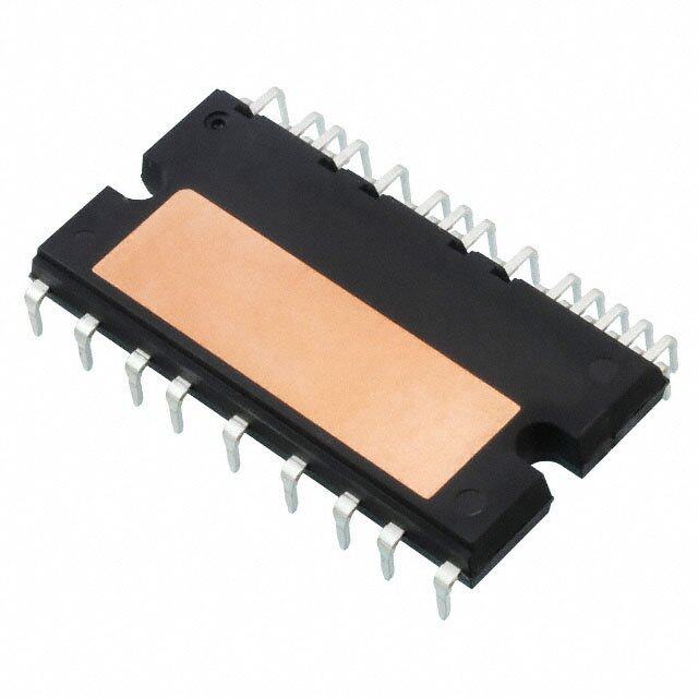
ICGOO电子元器件商城为您提供IRAM136-1061A2由International Rectifier设计生产,在icgoo商城现货销售,并且可以通过原厂、代理商等渠道进行代购。 IRAM136-1061A2价格参考。International RectifierIRAM136-1061A2封装/规格:功率驱动器模块, Power Driver Module IGBT 3 Phase 600V 12A 29-PowerSSIP Module, 21 Leads, Formed Leads。您可以下载IRAM136-1061A2参考资料、Datasheet数据手册功能说明书,资料中有IRAM136-1061A2 详细功能的应用电路图电压和使用方法及教程。
Infineon Technologies(英飞凌科技)的功率驱动器模块型号IRAM136-1061A2,是一款高度集成的智能功率模块(IPM),广泛应用于需要高效、可靠和紧凑设计的场景。以下是该型号的主要应用场景:

 1. 工业电机驱动
   - IRAM136-1061A2适用于各种工业电机驱动系统,例如伺服电机、变频器和风扇控制。其高效率和低功耗特性使其成为节能型电机驱动的理想选择。
   - 该模块支持三相逆变器拓扑结构,适合中小功率范围(通常为几百瓦到几千瓦)的电机应用。

 2. 家用电器
   - 在家用电器领域,IRAM136-1061A2常用于空调压缩机、洗衣机、冰箱等设备的电机驱动。其内置的保护功能(如过流、过热和欠压保护)可以显著提高系统的可靠性和安全性。
   - 该模块的小型化设计有助于降低家电产品的体积和重量,同时保持高性能。

 3. 新能源与绿色能源
   - 在太阳能逆变器和小型风力发电系统中,IRAM136-1061A2可用于将直流电转换为交流电(DC-AC转换)。其高效的功率转换能力和稳定的性能确保了能源的有效利用。
   - 此外,它还可用于电动汽车充电器中的功率转换部分,支持快速充电和高效能量传输。

 4. 机器人与自动化
   - 在工业机器人和自动化设备中,IRAM136-1061A2能够驱动精密电机,实现精确的位置控制和速度调节。其内置的驱动电路和保护功能简化了系统设计,降低了复杂性。
   - 该模块的高可靠性使其能够在严苛的工作环境中长时间运行。

 5. 医疗设备
   - 在某些医疗设备中(如呼吸机、泵类设备),IRAM136-1061A2可用于驱动关键部件的电机。其稳定性和低噪声特性对于医疗环境尤为重要。

 核心优势
- 集成度高:集成了IGBT、驱动电路和保护功能,减少了外部元件需求。
- 高效能:优化的热设计和低损耗特性提高了整体效率。
- 可靠性强:多重保护功能确保在异常情况下系统的安全运行。

综上所述,IRAM136-1061A2凭借其优异的性能和多功能性,适用于多种需要高效功率转换和可靠驱动的场景。
| 参数 | 数值 |
| 产品目录 | 集成电路 (IC)半导体 |
| 描述 | IC MOSFET DRIVER马达/运动/点火控制器和驱动器 10A-12A 600V ING PWR MODULE |
| 产品分类 | PMIC - 电机, 电桥式驱动器集成电路 - IC |
| 品牌 | International Rectifier |
| 产品手册 | |
| 产品图片 | |
| rohs | 符合RoHS无铅 / 符合限制有害物质指令(RoHS)规范要求 |
| 产品系列 | 电源管理 IC,马达/运动/点火控制器和驱动器,International Rectifier IRAM136-1061A2iMOTION™ |
| mouser_ship_limit | 该产品可能需要其他文件才能进口到中国。 |
| 数据手册 | |
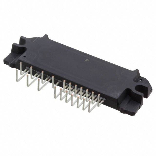
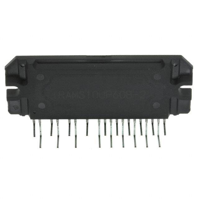
| 产品型号 | IRAM136-1061A2 |
| PCN组件/产地 | |
| 产品 | Fan / Motor Controllers / Drivers |
| 产品培训模块 | http://www.digikey.cn/PTM/IndividualPTM.page?site=cn&lang=zhs&ptm=26231http://www.digikey.cn/PTM/IndividualPTM.page?site=cn&lang=zhs&ptm=26250 |
| 产品种类 | 马达/运动/点火控制器和驱动器 |
| 供应商器件封装 | * |
| 功能 | 控制器 - 换向,方向管理 |
| 包装 | * |
| 商标 | International Rectifier |
| 安装类型 | * |
| 安装风格 | Through Hole |
| 封装 | Tube |
| 封装/外壳 | * |
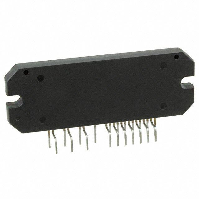
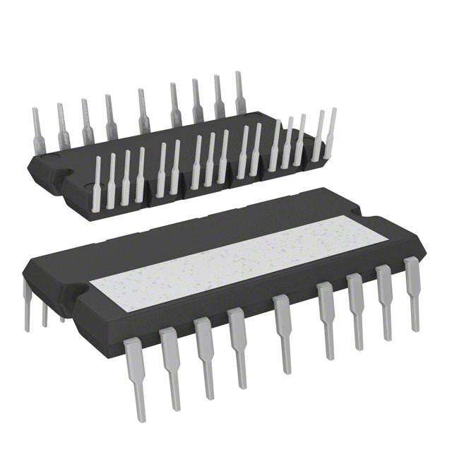
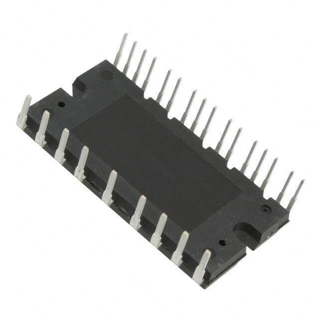
| 封装/箱体 | SIP-29 |
| 工作温度 | - 40 C to + 125 C |
| 工作电源电压 | 15 V |
| 工厂包装数量 | 80 |
| 应用 | 家电 |
| 接口 | 并联 |
| 标准包装 | 80 |
| 电压 | 600V |
| 电压-电源 | 13.5 V ~ 16.5 V |
| 电压-负载 | - |
| 电压-隔离 | 2000Vrms |
| 电机类型-AC,DC | AC, 3 相 |
| 电机类型-步进 | - |
| 电流 | 12A |
| 电流-输出 | - |
| 电源电流 | 120 uA |
| 类型 | Integrated Power Hybrid IC for Appliance Motor Drive Application |
| 输出配置 | 三相橋式, (1) 单 |
| 配置 | 3 相桥 |


- 商务部:美国ITC正式对集成电路等产品启动337调查
- 曝三星4nm工艺存在良率问题 高通将骁龙8 Gen1或转产台积电
- 太阳诱电将投资9.5亿元在常州建新厂生产MLCC 预计2023年完工
- 英特尔发布欧洲新工厂建设计划 深化IDM 2.0 战略
- 台积电先进制程称霸业界 有大客户加持明年业绩稳了
- 达到5530亿美元!SIA预计今年全球半导体销售额将创下新高
- 英特尔拟将自动驾驶子公司Mobileye上市 估值或超500亿美元
- 三星加码芯片和SET,合并消费电子和移动部门,撤换高东真等 CEO
- 三星电子宣布重大人事变动 还合并消费电子和移动部门
- 海关总署:前11个月进口集成电路产品价值2.52万亿元 增长14.8%
PDF Datasheet 数据手册内容提取
PD-97417 RevC IRAM136-1061A Series Integrated Power Hybrid IC for 10~12A, 600V Appliance Motor Drive Applications with Open Emitter Pins Description International Rectifier's IRAM136-1061A is a 10~12A, 600V Integrated Power Hybrid IC with Open Emitter pins for advanced Appliance Motor Drives applications such as energy efficient Washing Machine and Refrigerator Compressor Drivers. IR's technology offers an extremely compact, high performance AC motor- driver in a single isolated package to simplify design. This advanced HIC is a combination of IR's low V Trench IGBT technology and the industry benchmark CE (on) 3 phase high voltage, high speed driver (3.3V compatible) in a fully isolated thermally enhanced package. A built-in high precision temperature monitor and over-current protection feature, along with the short-circuit rated IGBTs and integrated under-voltage lockout function, deliver high level of protection and fail-safe operation. Using a Single in line package with full transfer mold structure and CTI>600 minimizes PCB space and resolves isolation problems to heatsink. Features (cid:2) Integrated gate drivers and bootstrap diodes (cid:2) Temperature monitor (cid:2) Protection shutdown pin (cid:2) Low V Trench IGBT technology CE (on) (cid:2) Undervoltage lockout for all channels (cid:2) Matched propagation delay for all channels (cid:2) 3.3V Schmitt-triggered input logic (cid:2) Cross-conduction prevention logic (cid:2) Motor Power range 0.25~0.75kW / 85~253 Vac (cid:2) Isolation 2000VRMS min and CTI> 600 (cid:2) RoHS Compliant (cid:2) Recognized by UL (File Number: E252584) Absolute Maximum Ratings V / V IGBT/ FW Diode Blocking Voltage 600 CES RRM V V+ Positive Bus Input Voltage 450 I @ T =25°C RMS Phase Current at F =16kHz (Note 1) 10 o C PWM I @ T =100°C RMS Phase Current at F =16kHz (Note 1) 5 o C PWM I @ T =25°C RMS Phase Current at F =6kHz (Note 1) 12 A o C PWM I @ T =100°C RMS Phase Current at F =6kHz (Note 1) 6 o C PWM I Maximum Peak Phase Current (Note 3) 15 pk F Maximum PWM Carrier Frequency 20 kHz p P Maximum Power dissipation per IGBT @ T =25°C 29 W d C V Isolation Voltage (1min) 2000 V ISO RMS T (IGBT & Diode & IC) Maximum Operating Junction Temperature +150 J T Operating Case Temperature Range -20 to +100 °C C T Storage Temperature Range -40 to +125 STG T Mounting torque Range (M3 screw) 0.8 to 1.0 Nm Note 1: Sinusoidal Modulation at V+=320V, V =15V, T=150°C, MI=0.8, PF=0.6, See Figure 4. CC J Note 2: t <100ms, V =15V, T =25°C, F =16kHz. P CC C PWM www.irf.com 1
IRAM136-1061A Internal Electrical Schematic – IRAM136-1061A V+ (13) Q1 D1 Q2 D2 Q3 D3 VRU (17) VRV (19) Q4 D4 Q5 D5 Q6 D6 VRW (21) R1 VB1 (9) C1 R2 R3 U, VS1 (10) VB2 (5) C2 V, VS2 (6) VB3 (1) C3 R4 R5 R6 W, VS3 (2) D9 D8 D7 22 21 20 19 18 17 23 VS1 VB2 HO2 VS2 VB3 HO3 VS3 LO1 16 24 HO1 R9 25 VB1 LO2 15 1 VCC Driver IC HIN1 (20) 2 HIN1 LO3 14 HIN2 (22) 3 HIN2 HIN3 (23) 4 HIN3LIN1LIN2LIN3 F ITRIP EN RCINVSSCOM 13 5 6 7 8 9 10 11 12 LIN1 (24) LIN2 (25) LIN3 (26) ITRIP (16) FLT/EN (18) R7 R8 VTH (27) C6 C5 VCC (28) C4 VSS (29) 2 www.irf.com
IRAM136-1061A Absolute Maximum Ratings (Continued) Symbol Parameter Min Max Units Conditions I Bootstrap Diode Peak Forward --- 1.0 A tP=10ms, BDF Current T=150°C, T =100°C J C Bootstrap Resistor Peak Power t=100μs, T =100°C P --- 15.0 W P C BR Peak (Single Pulse) ESR series High side floating supply offset V V - 20 V +0.3 V S1,2,3 voltage B1,2,3 B1,2,3 V High side floating supply voltage -0.3 600 V B1,2,3 Low Side and logic fixed supply V -0.3 20 V CC voltage Lower of Input voltage LIN, HIN, I , VIN FLT/EN Trip -0.3 (VSS+15V) or V VCC+0.3V Inverter Section Electrical Characteristics V (V , V )=15V, T=25ºC, unless otherwise specified. BIAS CC BS1,2,3 J Symbol Parameter Min Typ Max Units Conditions Collector-to-Emitter Breakdown V 600 --- --- V V =0V, I =250μA (BR)CES Voltage IN C Temperature Coeff. Of V =0V, I =250μA (cid:2)V / (cid:2)T --- 0.3 --- V/°C IN C (BR)CES Breakdown Voltage (25°C - 150°C) V Collector-to-Emitter Saturation --- 1.5 1.7 V IC=5A, TJ=25°C CE(ON) Voltage --- 1.7 2.1 I =5A, T=150°C C J Zero Gate Voltage Collector --- 5 80 V =0V, V+=600V I (cid:4)A IN CES Current --- 80 --- V =0V, V+=600V, T=150°C IN J -- 1.8 2.35 I=5A V Diode Forward Voltage Drop V F FM --- 1.45 1.8 I=5A, T=150°C F J V Bootstrap Diode Forward Voltage --- 1.65 1.8 V IF=1A BDFM Drop --- 1.3 --- I=1A, T=150°C F J R Bootstrap Resistor Value --- 22 --- (cid:3) T=25°C BR J (cid:2)R /R Bootstrap Resistor Tolerance --- --- ±5 % T=25°C BR BR J C V / V Capacitor Value --- 47 --- nF T=25°C 1,2,3,4 CC BS J C Itrip Capacitor Value --- 1 --- nF T=25°C 6 J www.irf.com 3
IRAM136-1061A Inverter Section Switching Characteristics V (V , V )=15V, T=25ºC, unless otherwise specified. BIAS CC BS1,2,3 J Symbol Parameter Min Typ Max Units Conditions EON Turn-On Switching Loss --- 240 400 IC=5A, V+=400V EOFF Turn-Off Switching Loss --- 65 90 VCC=15V, L=1.2mH μJ Energy losses include "tail" and E Total Switching Loss --- 305 490 TOT diode reverse recovery E Diode Reverse Recovery energy --- 15 25 REC tRR Diode Reverse Recovery time --- 115 --- ns See CT1 EON Turn-on Switching Loss --- 330 --- IC=5A, V+=400V EOFF Turn-off Switching Loss --- 105 --- VCC=15V, L=1.2mH, TJ=150°C μJ Energy losses include "tail" and E Total Switching Loss --- 435 --- TOT diode reverse recovery E Diode Reverse Recovery energy --- 40 --- REC tRR Diode Reverse Recovery time --- 150 --- ns See CT1 QG Turn-On IGBT Gate Charge --- 19 29 nC IC=8A, V+=400V, VGE=15V T=150°C, I =5A, V=600V J C P RBSOA Reverse Bias Safe Operating Area FULL SQUARE V+= 450V, V =+15V to 0V See CT3 CC T=25°C, V+= 400V, SCSOA Short Circuit Safe Operating Area 5 --- --- μs J V =+15V to 0V GE T=100°C, V+= 400V, SCSOA Short Circuit Safe Operating Area 3 --- --- μs J V =+15V to 0V GE T=150°C, V+= 360V, SCSOA Short Circuit Safe Operating Area 2 --- --- μs J V =+17.5V to 0V GE I Short Circuit Collector Current 11 --- --- A T=150°C, V = 50V, V =11V CSC J CE GE Recommended Operating Conditions Driver Function The Input/Output logic timing diagram is shown in Figure 1. For proper operation the device should be used within the recommended conditions. All voltages are absolute referenced to COM. The V offset is tested with all supplies biased at S 15V differential (Note 3) Symbol Definition Min Typ Max Units V High side floating supply voltage V+12.5 V+15 V +17.5 V B1,2,3 S S S V High side floating supply offset voltage Note 4 --- 450 V S1,2,3 V Low side and logic fixed supply voltage 13.5 15 16.5 V CC V I input voltage V --- V +5 V ITRIP TRIP SS SS V Logic input voltage LIN, HIN, FLT/EN V --- V +5 V IN SS SS HIN High side PWM pulse width 1 --- --- μs Deadtime External dead time between HIN and LIN 1 --- --- μs Note 3: For more details, see IR21364 data sheet Note 4: Logic operational for V from COM-5V to COM+600V. Logic state held for V from COM-5V to COM-V . s s BS (please refer to DT97-3 for more details) 4 www.irf.com
IRAM136-1061A Static Electrical Characteristics Driver Function V (V , V )=15V, T=25ºC, unless otherwise specified. The V and I parameters are referenced to COM and BIAS CC BS1,2,3 J IN IN are applicable to all six channels. (Note 3) Symbol Definition Min Typ Max Units V Positive going input threshold for LIN, HIN, FLT/EN 2.5 --- --- V IN,th+ V Negative going input threshold for LIN, HIN, FLT/EN --- --- 0.8 V IN,th- V V V /V supply undervoltage, Positive going threshold 10.6 11.1 11.6 V CCUV+, BSUV+ CC BS V V V /V supply undervoltage, Negative going threshold 10.4 10.9 11.4 V CCUV-, BSUV- CC BS V V V and V supply undervoltage lock-out hysteresis --- 0.2 --- V CCUVH, BSUVH CC BS I Quiescent V supply current --- --- 120 μA QBS BS I Quiescent V supply current --- --- 2.3 mA QCC CC I Offset Supply Leakage Current --- --- 50 μA LK I Input bias current V =3.3V for LIN, HIN, FLT/EN --- 100 195 μA IN+ IN I Input bias current V =0V for LIN, HIN, FLT/EN -1 -- --- μA IN- IN I I bias current V =3.3V --- 3.3 6 μA TRIP+ TRIP T/ITRIP I I bias current V =0V -1 --- --- μA TRIP- TRIP T/ITRIP V(I ) I threshold Voltage 0.44 0.49 0.54 V TRIP TRIP V(I HYS) I Input Hysteresis --- 0.07 --- V Trip, TRIP R Fault low on resistance --- 50 100 (cid:2) on_FLT Dynamic Electrical Characteristics V (V , V )=15V, T=25ºC, unless otherwise specified. Driver only timing unless otherwise specified. BIAS CC BS1,2,3 J Symbol Parameter Min Typ Max Units Conditions Input to Output propagation turn- T --- --- 1.15 μs ON on delay time (see fig.11) I =5A, V+=300V C Input to Output propagation turn- T --- --- 1.15 μs OFF off delay time (see fig. 11) T Input filter time (HIN,LIN) --- 310 --- ns V =0 or V =5V FILIN IN IN T Input filter time (FLT/EN) 100 200 --- ns V =0 or V =5V FILEN IN IN EN low to six switch turn-off T --- --- 1.35 μs V =0 or V =5V, V =0 EN propagation delay (see fig. 3) IN IN EN T I to Fault propagation delay 400 600 800 ns V =0 or V =5V, V =5V FLT TRIP IN IN ITRIP T I Blanking Time 100 150 --- ns V =0 or V =5V, V =5V BLT-ITRIP TRIP IN IN ITRIP I to six switch turn-off TITRIP pTrRoIPpagation delay (see fig. 2) --- --- 1.5 μs IC=5A, V+=300V Internal Dead Time injected by D 220 290 360 ns V =0 or V =5V T driver IN IN Matching Propagation Delay Time M --- 40 75 ns External dead time> 400ns T (On & Off) all channels T Post ITRIP to six switch turn-off 1.17 1.7 2.19 ms TC = 25°C FLT-CLR clear time (see fig. 2) 1 1.5 1.9 T = 100°C C www.irf.com 5
IRAM136-1061A Thermal and Mechanical Characteristics Symbol Parameter Min Typ Max Units Conditions R Thermal resistance, per IGBT --- 3.8 4.6 Inverter Operating Condition th(J-C) Flat, greased surface. Heatsink R Thermal resistance, per Diode --- 5.8 6.9 °C/W th(J-C) compound thermal conductivity Rth(C-S) Thermal resistance, C-S --- 0.1 --- 1W/mK CTI Comparative Tracking Index 600 --- --- V BKCurve Curvature of module backside 0 80 --- (cid:4)m Convex only I =5A , T =100°C L Maximum Load Cycle Number --- 1800 --- x1000 OUT RMS C CN T = 2s, T =8s ON OFF Internal NTC - Thermistor Characteristics Parameter Definition Min Typ Max Units Conditions R Resistance 44.65 47 49.35 k(cid:3) T = 25°C 25 C R Resistance 1.27 1.41 1.56 k(cid:3) T = 125°C 125 C B B-constant (25-50°C) 3989 4050 4111 k R = R e [B(1/T2 - 1/T1)] 2 1 Temperature Range -40 --- 125 °C Typ. Dissipation constant --- 1 --- mW/°C T = 25°C C Input-Output Logic Level Table VV++ FLT/EN I HIN1,2,3 LIN1,2,3 U,V,W TRIP 1 0 1 0 V+ HHoo HHIINN11,,22,,33 1 0 0 1 0 ((2200,,2222,,2233)) UU,,VV,,WW 1 0 0 0 Off IICC 1 0 1 1 Off DDrriivveerr ((1100,,66,,22)) LLIINN11,,22,,33 1 1 X X Off LLoo 0 X X X Off ((2244,,2255,,2266)) 6 www.irf.com
IRAM136-1061A Figure 1. Input/Output Timing Diagram HIN1,2,3 LIN1,2,3 50% 50% I TRIP T FLT 50% FLT U,V,W 50% 50% T T ITRIP FLT-CLR Figure 2. I Timing Waveform TRIP Figure 3. Output Enable Timing Diagram Note 5: The shaded area indicates that both high-side and low-side switches are off and therefore the half- bridge output voltage would be determined by the direction of current flow in the load. www.irf.com 7
IRAM136-1061A Module Pin-Out Description Pin Name Description 1 VB3 High Side Floating Supply Voltage 3 2 W,VS3 Output 3 - High Side Floating Supply Offset Voltage 3 na none 4 na none 5 VB2 High Side Floating Supply voltage 2 6 V,VS2 Output 2 - High Side Floating Supply Offset Voltage 7 na none 8 na none 9 VB1 High Side Floating Supply voltage 1 10 U,VS1 Output 1 - High Side Floating Supply Offset Voltage 11 na none 12 na none 13 V+ Positive Bus Input Voltage 14 na none 15 na none 16 I Current Protection Pin TRIP 17 VRU Low Side Emitter Connection - Phase 1 18 FLT/EN Fault Output and Enable Pin 19 VRV Low Side Emitter Connection - Phase 2 20 HIN1 Logic Input High Side Gate Driver - Phase 1 21 VRW Low Side Emitter Connection - Phase 3 22 HIN2 Logic Input High Side Gate Driver - Phase 2 23 HIN3 Logic Input High Side Gate Driver - Phase 3 24 LIN1 Logic Input Low Side Gate Driver - Phase 1 25 LIN2 Logic Input Low Side Gate Driver - Phase 2 26 LIN3 Logic Input Low Side Gate Driver - Phase 3 27 V Temperature Feedback TH 28 V +15V Main Supply CC 29 V Negative Main Supply SS 8 www.irf.com
IRAM136-1061A Typical Application Connection IRAM136-1061A 1 I R A M 1 3 6 - 1 0 6 1 A 2 9 1. Electrolytic bus capacitors should be mounted as close to the module bus terminals as possible to reduce ringing and EMI problems. Additional high frequency ceramic capacitor mounted close to the module pins will further improve performance. 2. In order to provide good decoupling between VCC-VSS and VB1,2,3-VS1,2,3 terminals, the capacitors shown connected between these terminals should be located very close to the module pins. Additional high frequency capacitors, typically 0.1μF, are strongly recommended. 3. Value of the boot-strap capacitors depends upon the switching frequency. Their selection should be made based on IR design tip DT04-4, application note AN-1044 or Figure 11. Bootstrap capacitor value must be selected to limit the power dissipation of the internal resistor in series with the VCC. (see maximum ratings Table on page 3). 4. After approx. 2ms the FAULT is reset. (see Dynamic Characteristics Table on page 5). 5. PWM generator must be disabled within Fault duration to guarantee shutdown of the system, overcurrent condition must be cleared before resuming operation. www.irf.com 9
IRAM136-1061A 12 A nt - 1101 e urr 9 C S 8 M R 7 e s a 6 h utput P 45 TTT CC=== 1 890000ºººCCC O 3 C m u 2 m xi 1 a M 0 0 2 4 6 8 10 12 14 16 18 20 PWM Switching Frequency - kHz Figure 4. Maximum Sinusoidal Phase Current vs. PWM Switching Frequency Sinusoidal Modulation, V+=400V, T=150°C, MI=0.8, PF=0.6, fmod=50Hz J 7 A nt - 6 e rr u C 5 S M R e 4 s a h P 3 F = 12kHz ut FPWM = 16kHz p PWM Out 2 FPWM = 20kHz m u m 1 xi a M 0 1 10 100 Modulation Frequency - Hz Figure 5. Maximum Sinusoidal Phase Current vs. Modulation Frequency Sinusoidal Modulation, V+=400V, T=150°C, T =100°C, MI=0.8, PF=0.6 J C 10 www.irf.com
IRAM136-1061A 100 80 W s- s 60 o L r e w Po 40 al ot T 20 I = 6A OUT I = 5A OUT I = 4A OUT 0 0 2 4 6 8 10 12 14 16 18 20 PWM Switching Frequency - kHz Figure 6. Total Power Losses vs. PWM Switching Frequency Sinusoidal Modulation, V+=400V, T=150°C, MI=0.8, PF=0.6, fmod=50Hz J 120 100 W s - 80 s o L r 60 e w o P al 40 F = 20kHz Tot FPPWWMM = 16kHz F = 12kHz 20 PWM 0 0 1 2 3 4 5 6 7 8 Output Phase Current - A RMS Figure 7. Total Power Losses vs. Output Phase Current Sinusoidal Modulation, V+=400V, T=150°C, MI=0.8, PF=0.6, fmod=50Hz J www.irf.com 11
IRAM136-1061A 160 C e - º 140 r u at er 120 p m e T e 100 s a C e F = 12kHz bl 80 PWM a F = 16kHz w PWM o F = 20kHz All 60 PWM x a M 40 0 1 2 3 4 5 6 7 8 Output Phase Current - A RMS Figure 8. Maximum Allowable Case Temperature vs. Output RMS Current per Phase Sinusoidal Modulation, V+=400V, T=150°C, MI=0.8, PF=0.6, fmod=50Hz J 160 T = 1.28 x T + 7.57 J avg Therm 150 C ° re - 140 u at r e p 130 m e T n 120 o cti n u 110 J T B G I 100 90 65 70 75 80 85 90 95 100 105 110 115 Internal Thermistor Temperature Equivalent Read Out - °C Figure 9. Estimated Maximum IGBT Junction Temperature vs. Thermistor Temperature Sinusoidal Modulation, V+=400V, Iphase=5Arms, fsw=16kHz, fmod=50Hz, MI=0.8, PF=0.6 12 www.irf.com
IRAM136-1061A 5.0 4.5 V e - g 4.0 a olt TTHERM RTHERM TTHERM RTHERM TTHERM RTHERM V °C k(cid:3) °C k(cid:3) °C k(cid:3) ut 3.5 -40 1747 25 47.00 90 3.972 O -35 1245 30 37.64 95 3.388 d- 3.0 -30 898.5 35 30.33 100 2.902 a e -25 655.8 40 24.59 105 2.494 R Pin 2.5 --2105 438640..09 4550 2106..0453 111105 21..185600 Max or -10 271.7 55 13.54 120 1.615 Avg. mist 2.0 -05 210568..52 6605 191.3.2218 112350 11..420286 Min r 5 122.3 70 7.798 135 1.076 e h 1.5 10 95.23 75 6.544 140 0.9447 T 15 74.73 80 5.518 145 0.8321 20 59.07 85 4.674 150 0.7349 1.0 -40 -30 -20 -10 0 10 20 30 40 50 60 70 80 90 100 110 120 130 Thermistor Temperature - °C Figure 10. Thermistor Readout vs. Temperature (4.7kohm pull-up resistor, 5V) and Normal Thermistor Resistance values vs. Temperature Table. 11.0 F 10(cid:3)F (cid:2) 10.0 or - 9.0 cit a 8.0 p a 6.8(cid:3)F C 7.0 p ra 6.0 st ot 5.0 4.7(cid:3)F o B d 4.0 3.3(cid:3)F e nd 3.0 e 2.2(cid:3)F m m 2.0 1.5(cid:3)F o c 1.0 e R 0.0 0 5 10 15 20 PWM Frequency - kHz Figure 11. Recommended Bootstrap Capacitor Value vs. Switching Frequency www.irf.com 13
IRAM136-1061A Figure 12. Switching Parameter Definitions Figure 12a. Input to Output propagation turn-on Figure 12b. Input to Output propagation turn-off delay time. delay time. Figure 12c. Diode Reverse Recovery. 14 www.irf.com
IRAM136-1061A V+ I Ho N Hin1,2,3 IC Driver U,V,W I O Lin1,2,3 Lo Figure CT1. Switching Loss Circuit V+ Hin1,2,3 Ho IN IC Driver U,V,W Lin1,2,3 I O Lo I o Figure CT2. S.C.SOA Circuit V+ Hin1,2,3 Ho IN IC Driver U,V,W I O Lin1,2,3 Lo I o Figure CT3. R.B.SOA Circuit www.irf.com 15
IRAM136-1061A Package Outline IRAM136-1061A missing pin : 3,4,7,8,11,12,14,15 note5 note3 (cid:2) note4 P 9DF00 IRAM136-1061A note2 (cid:4) (cid:5)(cid:6) (cid:7) note1: Unit Tolerance is +0.5mm, (cid:2)(cid:2)(cid:2) Unless Otherwise Specified. note2: Mirror Surface Mark indicates Pin1 Identification. note3: Part Number Marking. (cid:3) Characters Font in this drawing differs from (cid:2)(cid:2)(cid:2)(cid:2) Font shown on Module. note4: Lot Code Marking. Characters Font in this drawing differs from (cid:2)(cid:2)(cid:2)(cid:2) Font shown on Module. note5: "P" Character denotes Lead Free. Characters Font in this drawing differs from Font shown on Module. Dimensions in mm For mounting instruction see AN-1049 16 www.irf.com
IRAM136-1061A Package Outline IRAM136-1061A2 missing pin : 3,4,7,8,11,12,14,15 note5 note3 (cid:2) note4 P 9DF00 IRAM136-1061A2 (cid:4) (cid:5)(cid:6) note2 (cid:7) note1: Unit Tolerance is +0.5mm, (cid:2)(cid:2)(cid:2) Unless Otherwise Specified. note2: Mirror Surface Mark indicates Pin1 Identification. note3: Part Number Marking. Characters Font in this drawing differs from (cid:2)(cid:2)(cid:2)(cid:2) Font shown on Module. (cid:3) note4: Lot Code Marking. Characters Font in this drawing differs from (cid:2)(cid:2)(cid:2)(cid:2) Font shown on Module. note5: "P" Character denotes Lead Free. Characters Font in this drawing differs from Font shown on Module. Dimensions in mm For mounting instruction see AN-1049 Data and Specifications are subject to change without notice IR WORLD HEADQUARTERS: 233 Kansas St., El Segundo, California 90245, USA Tel: (310) 252-7105 TAC Fax: (310) 252-7903 Visit us at www.irf.com for sales contact information 2011-03-17 www.irf.com 17