 Datasheet下载
- 型号: FSB50450UD
- 制造商: Fairchild Semiconductor
- 库位|库存: xxxx|xxxx
- 要求:
| 数量阶梯 | 香港交货 | 国内含税 |
| +xxxx | $xxxx | ¥xxxx |
查看当月历史价格
查看今年历史价格
FSB50450UD产品简介:
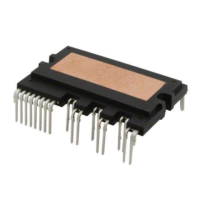
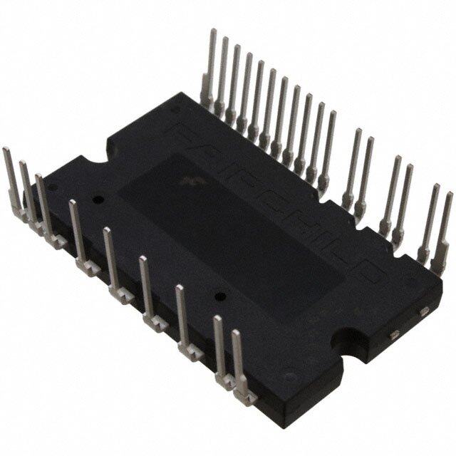
ICGOO电子元器件商城为您提供FSB50450UD由Fairchild Semiconductor设计生产,在icgoo商城现货销售,并且可以通过原厂、代理商等渠道进行代购。 FSB50450UD价格参考。Fairchild SemiconductorFSB50450UD封装/规格:功率驱动器模块, Power Driver Module MOSFET 3 Phase 500V 1.5A 23-PowerDIP Module (0.551", 14.00mm)。您可以下载FSB50450UD参考资料、Datasheet数据手册功能说明书,资料中有FSB50450UD 详细功能的应用电路图电压和使用方法及教程。
型号FSB50450UD是安森美半导体(ON Semiconductor)推出的一款功率驱动器模块,广泛应用于需要高效功率转换和电机控制的场景。该模块集成了高压栅极驱动器和高性能功率MOSFET,适用于中低功率的电机驱动、工业自动化、白色家电以及电源管理系统等领域。

其主要应用场景包括:

1. 电机控制:适用于交流感应电机、无刷直流电机(BLDC)和永磁同步电机(PMSM)的驱动控制,常见于家用电器如空调压缩机、洗衣机和风扇等。

2. 工业自动化设备:用于伺服驱动器、变频器和自动化控制系统中,提供高效、可靠的功率输出。

3. 电源系统:在UPS(不间断电源)、DC-AC逆变器及开关电源中作为功率转换模块使用。

4. 新能源应用:例如太阳能逆变器、储能系统中,用于实现高效的能量转换与管理。

FSB50450UD模块具备高集成度、良好的热性能和过流、过温保护功能,有助于提升系统效率与可靠性,同时简化电路设计,降低开发成本。
| 参数 | 数值 |
| 产品目录 | |
| 描述 | MOD SPM 500V 1.5A SPM23-HD马达/运动/点火控制器和驱动器 1.0A 500V SPM |
| 产品分类 | 功率驱动器 - 模块集成电路 - IC |
| 品牌 | Fairchild Semiconductor |
| 产品手册 | |
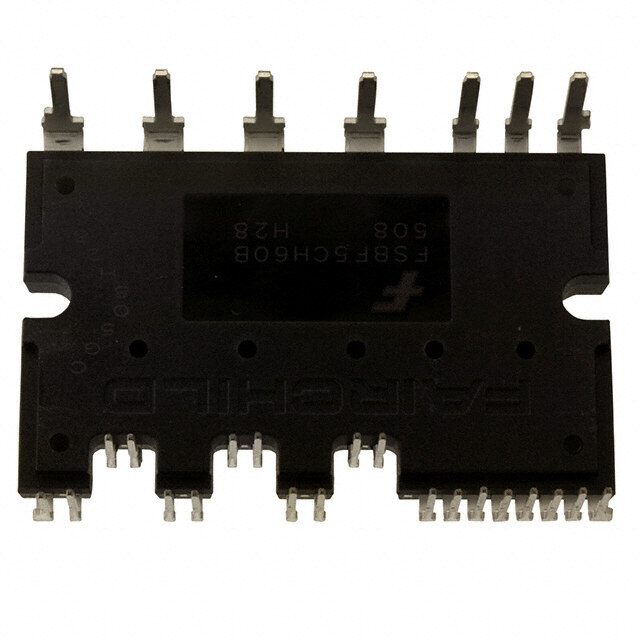
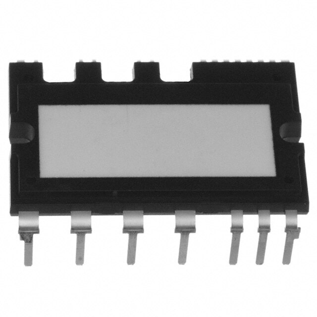
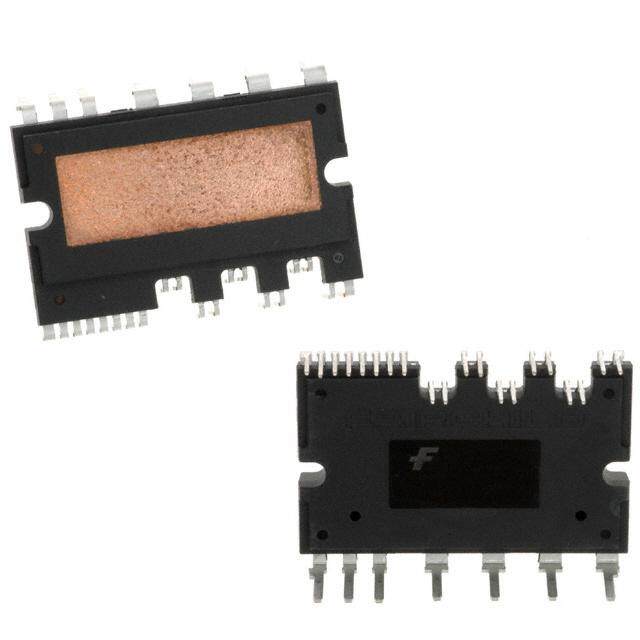
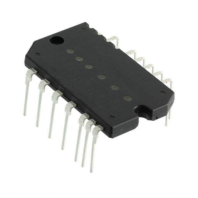
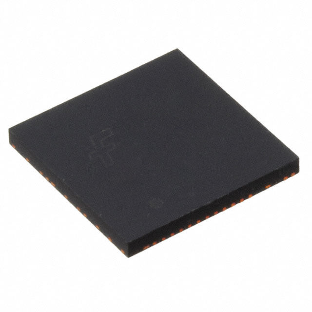
| 产品图片 |
|
| rohs | 符合RoHS无铅 / 符合限制有害物质指令(RoHS)规范要求 |
| 产品系列 | 电源管理 IC,马达/运动/点火控制器和驱动器,Fairchild Semiconductor FSB50450UDMotion-SPM® |
| 数据手册 | |
| 产品型号 | FSB50450UD |
| 产品种类 | 马达/运动/点火控制器和驱动器 |
| 单位重量 | 5.337 g |
| 商标 | Fairchild Semiconductor |
| 安装风格 | SMD/SMT |
| 封装 | Tube |
| 封装/外壳 | SPM23HD |
| 封装/箱体 | SPM23 |
| 工作温度 | - 40 C to + 125 C |
| 工作电源电压 | 15 V |
| 工厂包装数量 | 15 |
| 标准包装 | 15 |
| 电压 | 500V |
| 电压-隔离 | 1500Vrms |
| 电流 | 1.5A |
| 电源电流 | 160 uA |
| 类型 | 3 Half Bridge |
| 系列 | FSB50450 |
| 配置 | 3 相 |


- 商务部:美国ITC正式对集成电路等产品启动337调查
- 曝三星4nm工艺存在良率问题 高通将骁龙8 Gen1或转产台积电
- 太阳诱电将投资9.5亿元在常州建新厂生产MLCC 预计2023年完工
- 英特尔发布欧洲新工厂建设计划 深化IDM 2.0 战略
- 台积电先进制程称霸业界 有大客户加持明年业绩稳了
- 达到5530亿美元!SIA预计今年全球半导体销售额将创下新高
- 英特尔拟将自动驾驶子公司Mobileye上市 估值或超500亿美元
- 三星加码芯片和SET,合并消费电子和移动部门,撤换高东真等 CEO
- 三星电子宣布重大人事变动 还合并消费电子和移动部门
- 海关总署:前11个月进口集成电路产品价值2.52万亿元 增长14.8%

PDF Datasheet 数据手册内容提取
Is Now Part of To learn more about ON Semiconductor, please visit our website at www.onsemi.com Please note: As part of the Fairchild Semiconductor integration, some of the Fairchild orderable part numbers will need to change in order to meet ON Semiconductor’s system requirements. Since the ON Semiconductor product management systems do not have the ability to manage part nomenclature that utilizes an underscore (_), the underscore (_) in the Fairchild part numbers will be changed to a dash (-). This document may contain device numbers with an underscore (_). Please check the ON Semiconductor website to verify the updated device numbers. The most current and up-to-date ordering information can be found at www.onsemi.com. Please email any questions regarding the system integration to Fairchild_questions@onsemi.com. ON Semiconductor and the ON Semiconductor logo are trademarks of Semiconductor Components Industries, LLC dba ON Semiconductor or its subsidiaries in the United States and/or other countries. ON Semiconductor owns the rights to a number of patents, trademarks, copyrights, trade secrets, and other intellectual property. A listing of ON Semiconductor’s product/patent coverage may be accessed at www.onsemi.com/site/pdf/Patent-Marking.pdf. ON Semiconductor reserves the right to make changes without further notice to any products herein. ON Semiconductor makes no warranty, representation or guarantee regarding the suitability of its products for any particular purpose, nor does ON Semiconductor assume any liability arising out of the application or use of any product or circuit, and specifically disclaims any and all liability, including without limitation special, consequential or incidental damages. Buyer is responsible for its products and applications using ON Semiconductor products, including compliance with all laws, regulations and safety requirements or standards, regardless of any support or applications information provided by ON Semiconductor. “Typical” parameters which may be provided in ON Semiconductor data sheets and/or specifications can and do vary in different applications and actual performance may vary over time. All operating parameters, including “Typicals” must be validated for each customer application by customer’s technical experts. ON Semiconductor does not convey any license under its patent rights nor the rights of others. ON Semiconductor products are not designed, intended, or authorized for use as a critical component in life support systems or any FDA Class 3 medical devices or medical devices with a same or similar classification in a foreign jurisdiction or any devices intended for implantation in the human body. Should Buyer purchase or use ON Semiconductor products for any such unintended or unauthorized application, Buyer shall indemnify and hold ON Semiconductor and its officers, employees, subsidiaries, affiliates, and distributors harmless against all claims, costs, damages, and expenses, and reasonable attorney fees arising out of, directly or indirectly, any claim of personal injury or death associated with such unintended or unauthorized use, even if such claim alleges that ON Semiconductor was negligent regarding the design or manufacture of the part. ON Semiconductor is an Equal Opportunity/Affirmative Action Employer. This literature is subject to all applicable copyright laws and is not for resale in any manner.
F S B 5 0 4 January 2014 5 FSB50450UD 0 U D Motion SPM® 5 Series M o t i o Features Related Source n S • UL Certified No. E209204 (UL1557) • AN-9082 - Motion SPM5 Series Thermal Performance P by Contact Pressure M • 500 V R = 2.4 Max FRFET MOSFET 3-Phase DS(on) ® Inverter with Gate Drivers and Protection General Description 5 • Built-In Bootstrap Diodes Simplify PCB Layout S The FSB50450UD is an advanced Motion SPM® 5 e • Separate Open-Source Pins from Low-Side MOSFETs module providing a fully-featured, high-performance ri e for Three-Phase Current-Sensing inverter output stage for AC Induction, BLDC and PMSM s motors. These modules integrate optimized gate drive of • Active-HIGH Interface, Works with 3.3 / 5 V Logic, the built-in MOSFETs (FRFET® technology) to minimize Schmitt-trigger Input EMI and losses, while also providing multiple on-module • Optimized for Low Electromagnetic Interference protection features including under-voltage lockouts and • HVIC for Gate Driving and Under-Voltage Protection thermal monitoring. The built-in high-speed HVIC requires only a single supply voltage and • Isolation Rating: 1500 Vrms / min. translates the incoming logic-level gate inputs to the • RoHS Compliant high-voltage, high-current drive signals required to properly drive the module's internal MOSFETs. Applications Separate open-source MOSFET terminals are available for each phase to support the widest variety of control • 3-Phase Inverter Driver for Small Power AC Motor algorithms. Drives Package Marking & Ordering Information Device Device Marking Package Packing Type Quantity FSB50450UD FSB50450UD SPM5R-023 Rail 15 ©2010 Fairchild Semiconductor Corporation 1 www.fairchildsemi.com FSB50450UD Rev. C4
F S Absolute Maximum Ratings B 5 0 Inverter Part (each MOSFET unless otherwise specified.) 4 5 Symbol Parameter Conditions Rating Unit 0 U V Drain-Source Voltage of Each MOSFET 500 V D DSS *I Each MOSFET Drain Current, Continuous T = 25°C 1.5 A M D 25 C o *ID 80 Each MOSFET Drain Current, Continuous TC = 80°C 1.1 A t i o *I Each MOSFET Drain Current, Peak T = 25°C, PW < 100 s 3.8 A DP C n *P Maximum Power Dissipation T = 25°C, For Each MOSFET 14 W S D C P M Control Part (each HVIC unless otherwise specified.) ® 5 Symbol Parameter Conditions Rating Unit S V Control Supply Voltage Applied Between V and COM 20 V e CC CC r i V High-side Bias Voltage Applied Between V and V 20 V e BS B S s V Input Signal Voltage Applied Between IN and COM -0.3 ~ V + 0.3 V IN CC Bootstrap Diode Part (each bootstrap diode unless otherwise specified.) Symbol Parameter Conditions Rating Unit VRRMB Maximum Repetitive Reverse Voltage 500 V * I Forward Current T = 25°C 0.5 A FB C * IFPB Forward Current (Peak) TC = 25°C, Under 1ms Pulse Width 2.0 A Thermal Resistance Symbol Parameter Conditions Rating Unit Each MOSFET under Inverter Oper- R Junction to Case Thermal Resistance 8.9 °C/W JC ating Condition (1st Note 1) Total System Symbol Parameter Conditions Rating Unit T Operating Junction Temperature -40 ~ 150 °C J T Storage Temperature -40 ~ 125 °C STG 60 Hz, Sinusoidal, 1 Minute, Con- V Isolation Voltage 1500 V ISO nect Pins to Heat Sink Plate rms 1st Notes: 1. For the measurement point of case temperature TC, please refer to Figure 4. 2. Marking “ * “ is calculation value or design factor. ©2010 Fairchild Semiconductor Corporation 2 www.fairchildsemi.com FSB50450UD Rev. C4
F S Pin descriptions B 5 0 Pin Number Pin Name Pin Description 4 5 1 COM IC Common Supply Ground 0 U 2 V Bias Voltage for U Phase High Side MOSFET Driving D B(U) 3 VCC(U) Bias Voltage for U Phase IC and Low Side MOSFET Driving M 4 IN Signal Input for U Phase High-Side o (UH) t i 5 IN Signal Input for U Phase Low-Side o (UL) n 6 VS(U) Bias Voltage Ground for U Phase High Side MOSFET Driving S P 7 V Bias Voltage for V Phase High Side MOSFET Driving B(V) M 8 V Bias Voltage for V Phase IC and Low Side MOSFET Driving ® CC(V) 9 IN Signal Input for V Phase High-Side 5 (VH) S 10 IN(VL) Signal Input for V Phase Low-Side e r 11 VS(V) Bias Voltage Ground for V Phase High Side MOSFET Driving ie s 12 VB(W) Bias Voltage for W Phase High Side MOSFET Driving 13 V Bias Voltage for W Phase IC and Low Side MOSFET Driving CC(W) 14 IN Signal Input for W Phase High-Side (WH) 15 IN Signal Input for W Phase Low-Side (WL) 16 V Bias Voltage Ground for W Phase High Side MOSFET Driving S(W) 17 P Positive DC–Link Input 18 U Output for U Phase 19 N Negative DC–Link Input for U Phase U 20 N Negative DC–Link Input for V Phase V 21 V Output for V Phase 22 N Negative DC–Link Input for W Phase W 23 W Output for W Phase (1) COM (2) VB(U) (17) P (3) VCC(U) VCC VB (4) IN(UH) HIN HO (5) IN(UL) LIN VS (18) U COM LO ((67)) VVSB((VU)) (19) NU (8) VCC(V) VCC VB (20) NV (9) IN(VH) HIN HO (10) IN(VL) LIN VS (21) V COM LO (11) VS(V) (12) VB(W) (13) VCC(W) VCC VB (22) NW (14) IN(WH) HIN HO (15) IN(WL) LIN VS (23) W COM LO (16) VS(W) Figure 1. Pin Configuration and Internal Block Diagram (Bottom View) 1st Notes: 3. Source terminal of each low-side MOSFET is not connected to supply ground or bias voltage ground inside Motion SPM® 5 product. External connections should be made as indicated in Figure 3. ©2010 Fairchild Semiconductor Corporation 3 www.fairchildsemi.com FSB50450UD Rev. C4
F S Electrical Characteristics B (T = 25°C, V = V = 15 V unless otherwise specified.) J CC BS 5 0 Inverter Part (each MOSFET unless otherwise specified.) 4 5 Symbol Parameter Conditions Min Typ Max Unit 0 U Drain - Source D BVDSS Breakdown Voltage VIN = 0 V, ID = 250 A (2nd Note 1) 500 - - V M BV / Breakdown Voltage Tem- o TDJSS perature Coefficient ID = 250A, Referenced to 25°C - 0.53 - V tio Zero Gate Voltage n IDSS Drain Current VIN = 0 V, VDS = 500 V - - 250 A S P Static Drain - Source M R V = V = 15 V, V = 5 V, I = 0.5 A - 1.9 2.4 DS(on) Turn-On Resistance CC BS IN D ® Drain - Source Diode 5 V V = V = 15V, V = 0 V, I = -0.5 A - - 1.2 V SD Forward Voltage CC BS IN D S e t - 1250 - ns r ON i e tOFF VVPN = = 0 3 V00 V ,5 V VC,C I n=d VucBtSiv =e 1L5o aVd, ILD == 30 .m5 HA - 500 - ns s t Switching Times IN - 200 - ns rr High- and Low-Side MOSFET Switching EON (2nd Note 2) - 80 - J E - 10 - J OFF V = 400 V, V = V = 15 V, I = I , V = BV , Reverse Bias Safe Oper- PN CC BS D DP DS DSS RBSOA T = 150°C Full Square ating Area J High- and Low-Side MOSFET Switching (2nd Note 3) Control Part (each HVIC unless otherwise specified.) Symbol Parameter Conditions Min Typ Max Unit V = 15 V, I Quiescent V Current CC Applied Between V and COM - - 160 A QCC CC V = 0 V CC IN V = 15 V, Applied Between V - U, I Quiescent V Current BS B(U) - - 100 A QBS BS V = 0 V V - V, V - W IN B(V) B(W) UVCCD Low-Side Under-Voltage VCC Under-Voltage Protection Detection Level 7.4 8.0 9.4 V UV Protection (Figure 8) V Under-Voltage Protection Reset Level 8.0 8.9 9.8 V CCR CC UVBSD High-Side Under-Voltage VBS Under-Voltage Protection Detection Level 7.4 8.0 9.4 V UV Protection (Figure 9) V Under-Voltage Protection Reset Level 8.0 8.9 9.8 V BSR BS V ON Threshold Voltage Logic High Level 2.9 - - V IH Applied between IN and COM V OFF Threshold Voltage Logic Low Level - - 0.8 V IL I V = 5V - 10 20 A IH IN Input Bias Current Applied between IN and COM I V = 0V - - 2 A IL IN Bootstrap Diode Part (each bootstrap diode unless otherwise specified.) Symbol Parameter Conditions Min Typ Max Unit V Forward Voltage I = 0.1 A, T = 25°C (2nd Note 5) - 2.0 - V FB F C t Reverse Recovery Time I = 0.1 A, T = 25°C - 80 - ns rrB F C 2nd Notes: 1. BVDSS is the absolute maximum voltage rating between drain and source terminal of each MOSFET inside Motion SPM® 5 product. VPN should be sufficiently less than this value considering the effect of the stray inductance so that VPN should not exceed BVDSS in any case. 2. tON and tOFF include the propagation delay of the internal drive IC. Listed values are measured at the laboratory test condition, and they can be different according to the field applications due to the effect of different printed circuit boards and wirings. Please see Figure 5 for the switching time definition with the switching test circuit of Figure 6. 3. The peak current and voltage of each MOSFET during the switching operation should be included in the Safe Operating Area (SOA). Please see Figure 6 for the RBSOA test circuit that is same as the switching test circuit. 4. Built-in bootstrap diode includes around 15Ωresistance characteristic. Please refer to Figure 2. ©2010 Fairchild Semiconductor Corporation 4 www.fairchildsemi.com FSB50450UD Rev. C4
F S Recommended Operating Condition B 5 0 Symbol Parameter Conditions Min. Typ. Max. Unit 4 5 0 V Supply Voltage Applied Between P and N - 300 400 V PN U V Control Supply Voltage Applied Between V and COM 13.5 15.0 16.5 V D CC CC V High-Side Bias Voltage Applied Between V and V 13.5 15.0 16.5 V M BS B S o VIN(ON) Input ON Threshold Voltage 3.0 - VCC V t Applied Between IN and COM io V Input OFF Threshold Voltage 0 - 0.6 V IN(OFF) n Blanking Time for Preventing S tdead Arm-Short VCC = VBS = 13.5 ~ 16.5 V, TJ 150°C 1.0 - - s P M fPWM PWM Switching Frequency TJ 150°C - 15 - kHz ® 5 S e r i e Built-in Bootstrap Diode V-I Characteristic s F F 1.0 0.9 0.8 0.7 0.6 A] 0.5 [F I 0.4 0.3 0.2 0.1 0.0 0 1 2 3 4 5 6 7 8 9 10 11 12 13 14 15 V [V] F Tc=25°C Figure 2. Built-in Bootstrap Diode Characteristics (Typical) ©2010 Fairchild Semiconductor Corporation 5 www.fairchildsemi.com FSB50450UD Rev. C4
F S B 5 0 These Values Depend on PWM 4 15V Control Algorithm * Example Circuit : V phase 5 Line 0 One Leg Diagram of Motion SPM® 5 Product U VDC D P om R5 VHCINC HVOB V OInuvteprutetr H0IN L0IN OuZtput Both FNRoFteETOff Mo Mic C1 LIN VS C3 0 1 0 Low side FRFET On tio C5 COM LO N R3 1 0 VDC High side FRFET On n 1 1 Forbidden Shoot through S P 10F C2 Open Open Z Same as(0,0) M ® * Example of Bootstrap Param:ters C = C = 1 F Ceramic Capacitor 5 1 2 S e r i Figure 3. Recommended MCU Interface and Bootstrap Circuit with Parameters e s 3rd Notes: 1. Parameters for bootstrap circuit elements are dependent on PWM algorithm. For 15 kHz of switching frequency, typical example of parameters is shown above. 2. RC-coupling (R5 and C5) and C4 at each input of Motion SPM 5 product and MCU (Indicated as Dotted Lines) may be used to prevent improper signal due to surge-noise. 3. Bold lines should be short and thick in PCB pattern to have small stray inductance of circuit, which results in the reduction of surge-voltage. Bypass capacitors such as C1, C2 and C3 should have good high-frequency characteristics to absorb high-frequency ripple-current. 1144..5500mmmm 33..8800mmmm CCaassee TTeemmppeerraattuurree((TTcc)) MMOOSSFFEETT DDeetteeccttiinngg PPooiinntt Figure 4. Case Temperature Measurement 3rd Notes: 4. Attach the thermocouple on top of the heat-sink of SPM 5 package (between SPM 5 package and heatsink if applied) to get the correct temperature measurement. ©2010 Fairchild Semiconductor Corporation 6 www.fairchildsemi.com FSB50450UD Rev. C4
F S B 5 0 4 V V IN IN 5 I 0 rr 100% of ID 120% of ID UD V I DS D M o 10% of I t D i I V o D DS n S P t t t ON rr OFF M ® (a) Turn-on (b) Turn-off 5 S Figure 5. Switching Time Definitions e r i e s V One-leg Diagram of Motion SPM® 5 Product I CC D VCC VB L V HIN HO DC LIN VS + CBS COM LO V-DS Figure 6. Switching and RBSOA (Single-pulse) Test Circuit (Low-side) Input Signal UV Protection RESET DETECTION RESET Status UV Low-side Supply, V CCR CC UV CCD MOSFET Current Figure 7. Under-Voltage Protection (Low-Side) Input Signal UV Protection RESET DETECTION RESET Status UV High-side Supply, V BSR BS UV BSD MOSFET Current Figure 8. Under-Voltage Protection (High-Side) ©2010 Fairchild Semiconductor Corporation 7 www.fairchildsemi.com FSB50450UD Rev. C4
F S B 5 0 R2 4 5 0 U D (1) COM (2) VB(U) (17) P M o (3) VCC(U) VCC VB ti R5 (4) IN(UH) HIN HO (18) U on (5) IN(UL) LIN VS S C3 VDC P C5 C2 C1 COM LO M (6) VS(U) (19) NU ® (7) VB(V) 5 (8) VCC(V) VCC VB (20) NV S (9) IN(VH) e om (10) IN(VL) HLIINN HVOS (21) V M rie c s Mi C2 C1 COM LO (11) VS(V) (12) VB(W) (13) VCC(W) (22) NW VCC VB (14) IN(WH) HIN HO (23) W (15) IN(WL) LIN VS C2 C1 COM LO (16) VS(W) For 3-phase current sensing and protection R4 15-V Supply C4 R3 Figure 9. Example of Application Circuit 4th Notes: 1. About pin position, refer to Figure 1. 2. RC-coupling (R5 and C5, R4 and C6) and C4 at each input of Motion SPM® 5 product and MCU are useful to prevent improper input signal caused by surge-noise. 3. The voltage-drop across R3 affects the low-side switching performance and the bootstrap characteristics since it is placed between COM and the source terminal of the low- side MOSFET. For this reason, the voltage-drop across R3 should be less than 1 V in the steady-state. 4. Ground-wires and output terminals, should be thick and short in order to avoid surge-voltage and malfunction of HVIC. 5. All the filter capacitors should be connected close to Motion SPM 5 product, and they should have good characteristics for rejecting high-frequency ripple current. ©2010 Fairchild Semiconductor Corporation 8 www.fairchildsemi.com FSB50450UD Rev. C4
F S Detailed Package Outline Drawings B 5 0 4 5 0 U D M o t i o n S P M ® 5 S e r i e s Package drawings are provided as a service to customers considering Fairchild components. Drawings may change in any manner without notice. Please note the revision and/or data on the drawing and contact a FairchildSemiconductor representative to verify or obtain the most recent revision. Package specifications do not expand the terms of Fairchild’s worldwide therm and conditions, specifically the the warranty therein, which covers Fairchild products. Always visit Fairchild Semiconductor’s online packaging area for the most recent package drawings: http://www.fairchildsemi.com/dwg/MO/MOD23DB.pdf ©2010 Fairchild Semiconductor Corporation 9 www.fairchildsemi.com FSB50450UD Rev. C4
F S B 5 0 4 5 0 U D M o t i o n S P M ® 5 S e r i e s ©2010 Fairchild Semiconductor Corporation 10 www.fairchildsemi.com FSB50450UD Rev. C4
ON Semiconductor and are trademarks of Semiconductor Components Industries, LLC dba ON Semiconductor or its subsidiaries in the United States and/or other countries. ON Semiconductor owns the rights to a number of patents, trademarks, copyrights, trade secrets, and other intellectual property. A listing of ON Semiconductor’s product/patent coverage may be accessed at www.onsemi.com/site/pdf/Patent−Marking.pdf. ON Semiconductor reserves the right to make changes without further notice to any products herein. ON Semiconductor makes no warranty, representation or guarantee regarding the suitability of its products for any particular purpose, nor does ON Semiconductor assume any liability arising out of the application or use of any product or circuit, and specifically disclaims any and all liability, including without limitation special, consequential or incidental damages. Buyer is responsible for its products and applications using ON Semiconductor products, including compliance with all laws, regulations and safety requirements or standards, regardless of any support or applications information provided by ON Semiconductor. “Typical” parameters which may be provided in ON Semiconductor data sheets and/or specifications can and do vary in different applications and actual performance may vary over time. All operating parameters, including “Typicals” must be validated for each customer application by customer’s technical experts. ON Semiconductor does not convey any license under its patent rights nor the rights of others. ON Semiconductor products are not designed, intended, or authorized for use as a critical component in life support systems or any FDA Class 3 medical devices or medical devices with a same or similar classification in a foreign jurisdiction or any devices intended for implantation in the human body. Should Buyer purchase or use ON Semiconductor products for any such unintended or unauthorized application, Buyer shall indemnify and hold ON Semiconductor and its officers, employees, subsidiaries, affiliates, and distributors harmless against all claims, costs, damages, and expenses, and reasonable attorney fees arising out of, directly or indirectly, any claim of personal injury or death associated with such unintended or unauthorized use, even if such claim alleges that ON Semiconductor was negligent regarding the design or manufacture of the part. ON Semiconductor is an Equal Opportunity/Affirmative Action Employer. This literature is subject to all applicable copyright laws and is not for resale in any manner. PUBLICATION ORDERING INFORMATION LITERATURE FULFILLMENT: N. American Technical Support: 800−282−9855 Toll Free ON Semiconductor Website: www.onsemi.com Literature Distribution Center for ON Semiconductor USA/Canada 19521 E. 32nd Pkwy, Aurora, Colorado 80011 USA Europe, Middle East and Africa Technical Support: Order Literature: http://www.onsemi.com/orderlit Phone: 303−675−2175 or 800−344−3860 Toll Free USA/Canada Phone: 421 33 790 2910 Fax: 303−675−2176 or 800−344−3867 Toll Free USA/Canada Japan Customer Focus Center For additional information, please contact your local Email: orderlit@onsemi.com Phone: 81−3−5817−1050 Sales Representative © Semiconductor Components Industries, LLC www.onsemi.com www.onsemi.com 1
Mouser Electronics Authorized Distributor Click to View Pricing, Inventory, Delivery & Lifecycle Information: O N Semiconductor: FSB50450UD