ICGOO在线商城 > IL611-1E
 Datasheet下载
- 型号: IL611-1E
- 制造商: NVE Corporation
- 库位|库存: xxxx|xxxx
- 要求:
| 数量阶梯 | 香港交货 | 国内含税 |
| +xxxx | $xxxx | ¥xxxx |
查看当月历史价格
查看今年历史价格
IL611-1E产品简介:
ICGOO电子元器件商城为您提供IL611-1E由NVE Corporation设计生产,在icgoo商城现货销售,并且可以通过原厂、代理商等渠道进行代购。 提供IL611-1E价格参考以及NVE CorporationIL611-1E封装/规格参数等产品信息。 你可以下载IL611-1E参考资料、Datasheet数据手册功能说明书, 资料中有IL611-1E详细功能的应用电路图电压和使用方法及教程。
NVE Corp/Isolation Products 的 IL611-1E 是一款基于巨磁阻(GMR)技术的单通道数字隔离器,具有高可靠性、低功耗和强抗干扰能力。其典型应用场景包括:

- 工业自动化与控制系统:用于PLC、DCS、I/O模块中隔离微控制器与现场总线(如RS-485、CAN)或执行器接口,防止地环路噪声和高压瞬变损坏敏感电路。

- 电机驱动与变频器:隔离栅极驱动信号(如IGBT/SiC驱动),确保控制侧与高压功率侧电气隔离,满足IEC 61800-5-1等安全标准。

- 医疗电子设备:在患者连接设备(如监护仪、透析机)中实现信号链隔离,保障患者安全(符合IEC 60601-1的2×MOPP隔离要求,IL611-1E通过UL/VDE/CSA认证,隔离耐压达5kVRMS)。

- 新能源系统:用于光伏逆变器、储能BMS中隔离ADC采样信号、MCU通信(SPI/I²C)或故障反馈信号,提升系统在高dv/dt环境下的稳定性。

- 测试测量仪器:在高精度数据采集系统中隔离数字通信线路,抑制共模噪声,提高信噪比与测量准确性。

该器件工作温度范围宽(–40°C 至 +105°C),传播延迟低(典型值15 ns),支持高达100 Mbps数据速率,且无需外部电源隔离(集成隔离DC-DC转换器),简化系统设计。适用于对安全性、长期稳定性和EMC性能要求严苛的工业及医疗场景。
| 参数 | 数值 |
| 产品目录 | |
| ChannelType | 单向 |
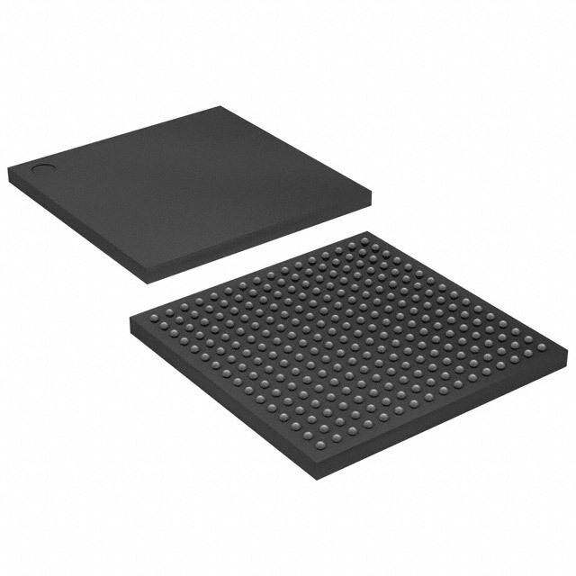
| 描述 | IC DGTL ISO 2CH CMOS 8MSOP |
| 产品分类 | |
| IsolatedPower | 无 |
| 品牌 | NVE Corp/Isolation Products |
| 数据手册 | |
| 产品图片 |
|
| 产品型号 | IL611-1E |
| PulseWidthDistortion(Max) | 5ns |
| rohs | 无铅 / 符合限制有害物质指令(RoHS)规范要求 |
| 产品系列 | IsoLoop® |
| 上升/下降时间(典型值) | 2ns, 2ns |
| 产品培训模块 | http://www.digikey.cn/PTM/IndividualPTM.page?site=cn&lang=zhs&ptm=25405 |
| 产品目录绘图 |
|
| 产品目录页面 | |
| 传播延迟tpLH/tpHL(最大值) | 15ns, 15ns |
| 供应商器件封装 | 8-MSOP |
| 共模瞬态抗扰度(最小值) | 15kV/µs |
| 其它名称 | 390-1081-5 |
| 包装 | 管件 |
| 封装/外壳 | 8-TSSOP,8-MSOP(0.118",3.00mm 宽) |
| 工作温度 | -40°C ~ 85°C |
| 技术 | GMR(大型磁阻传感) |
| 数据速率 | 100Mbps |
| 标准包装 | 100 |
| 电压-电源 | 3 V ~ 5.5 V |
| 电压-隔离 | 2500Vrms |
| 类型 | 通用 |
| 脉宽失真(最大) | 5ns |
| 输入-输入侧1/输入侧2 | 2/0 |
| 通道数 | 2 |
| 通道类型 | 单向 |
| 隔离式电源 | 无 |


- 商务部:美国ITC正式对集成电路等产品启动337调查
- 曝三星4nm工艺存在良率问题 高通将骁龙8 Gen1或转产台积电
- 太阳诱电将投资9.5亿元在常州建新厂生产MLCC 预计2023年完工
- 英特尔发布欧洲新工厂建设计划 深化IDM 2.0 战略
- 台积电先进制程称霸业界 有大客户加持明年业绩稳了
- 达到5530亿美元!SIA预计今年全球半导体销售额将创下新高
- 英特尔拟将自动驾驶子公司Mobileye上市 估值或超500亿美元
- 三星加码芯片和SET,合并消费电子和移动部门,撤换高东真等 CEO
- 三星电子宣布重大人事变动 还合并消费电子和移动部门
- 海关总署:前11个月进口集成电路产品价值2.52万亿元 增长14.8%


PDF Datasheet 数据手册内容提取
IL600 Series Isolators Passive-Input Digital Isolators – CMOS Outputs Functional Diagrams Features Up to 100 Mbps data rate VOE Flexible inputs with very wide input voltage range 5 mA input current IN1 OUT1 Failsafe output (logic high output for zero coil current) No carrier or clock for low EMI emissions and susceptibility Low power dissipation IL610 3 V to 5 V power supplies 1000 V /1500 V high voltage endurance RMS DC 44000 year barrier life IN OUT −40°C to 85°C temperature range 1 1 UL 1577 recognized; IEC 60747-5-5 (VDE 0884) certified IN OUT 8-pin MSOP, SOIC, and PDIP packages 2 2 0.15", 0.3", or True 8™ mm SOIC packages IL611 Applications CAN Bus / Device Net VDD1 Differential line receiver OUT IN 1 Optocoupler replacement 1 VDD2 SPI interface OUT 2 IN RS-485, RS-422, or RS-232 2 Digital Fieldbus IL612 Space-critical multi-channel applications Description IN1 OUT1 The IL600 Series are passive input digital signal isolators with CMOS outputs. They have a similar interface but better IN2 OUT2 performance and higher package density than optocouplers. The devices are manufactured with NVE’s patented* IN OUT 3 3 IsoLoop® spintronic Giant Magnetoresistive (GMR) technology for small size, high speed, and low power. IL613 A unique ceramic/polymer composite barrier provides excellent isolation and virtually unlimited barrier life. A resistor sets the input current; a capacitor in parallel with OUT 1 IN V 1 the current-limit resistor provides improved dynamic OE performance. IN2 OUT2 These versatile components simplify inventory requirements COIL OUT by replacing a variety of optocouplers, functioning over a 3 IN wide range of data rates, edge speeds, and power supply 3 levels. The devices are available in various packages, as well IL614 as bare die. IsoLoop is a registered trademark of NVE Corporation. REV. AC *U.S. Patent number 5,831,426; 6,300,617 and others. NVE Corporation 11409 Valley View Road, Eden Prairie, MN 55344-3617 Phone: (952) 829-9217 Fax: (952) 829-9189 www.IsoLoop.com ©NVE Corporation
IL600 Series Isolators Absolute Maximum Ratings(1) Parameters Symbol Min. Typ. Max. Units Test Conditions Storage Temperature T −55(2) 150 °C S Ambient Operating Temperature T −40(3) 85 °C A Supply Voltage V −0.5 7 V DD DC Input Current I −25 25 mA IN AC Input Current (Single-Ended I −35 35 mA Input) IN AC Input Current (Differential Input) I −75 75 mA IN Output Voltage V −0.5 V +1.5 V O DD Maximum Output Current I −10 10 mA O ESD 2 kV HBM Note 1: Operating at absolute maximum ratings will not damage the device. Parametric performance is not guaranteed at absolute maximum ratings. Note 2: -55oC applies to all except IL611-1E. -20oC applies to IL611-1E Note 3: -40oC applies to all except IL611-1E. -20oC applies to IL611-1E Recommended Operating Conditions Parameters Symbol Min. Typ. Max. Units Test Conditions Ambient Operating Temperature T −40(3) 85 °C A Supply Voltage V 3.0 5.5 V DD Output Current I −4 4 mA OUT Common Mode Input Voltage V 400 V CM RMS Insulation Specifications Parameters Symbol Min. Typ. Max. Units Test Conditions Creepage Distance (external) MSOP 3.01 mm 0.15'' SOIC 4.03 mm 0.3'' SOIC 8.03 8.3 mm Per IEC 60601 PDIP 7.08 mm Total Barrier Thickness (internal) 0.012 0.013 mm Leakage Current 0.2 μA 240 V , 60 Hz RMS Barrier Resistance R >1014 500 V IO Barrier Capacitance C 7 Ω || pF f = 1 MHz IO Comparative Tracking Index CTI ≥175 V Per IEC 60112 High Voltage Endurance AC 1000 V RMS At maximum (Maximum Barrier Voltage V IO operating temperature for Indefinite Life) DC 1500 V DC 100°C, 1000 V , 60% Barrier Life 44000 Years RMS CL activation energy 2 NVE Corporation 11409 Valley View Road, Eden Prairie, MN 55344-3617 Phone: (952) 829-9217 Fax: (952) 829-9189 www.IsoLoop.com ©NVE Corporation
IL600 Series Isolators Safety and Approvals IEC 60747-5-5 (VDE 0884) (File Number 5016933-4880-0001) Working Voltage (VIORM) 600 VRMS (848 VPK); basic insulation; pollution degree 2 Transient overvoltage (VIOTM) and surge voltage (VIOSM) 4000 VPK Each part tested at 1590 VPK for 1 second, 5 pC partial discharge limit Samples tested at 4000 VPK for 60 sec.; then 1358 VPK for 10 sec. with 5 pC partial discharge limit IEC 61010-1 (Edition 2; TUV Certificate Numbers N1502812; N1502812-101) Reinforced Insulation; Pollution Degree II; Material Group III Part No. Suffix Package Working Voltage -1 MSOP 150 VRMS -2 PDIP 300 VRMS -3 SOIC 150 VRMS None Wide-body SOIC/True 8™ 300 VRMS UL 1577 (Component Recognition Program File Number E207481) Each part other than MSOP tested at 3000 VRMS (4240 VPK) for 1 second; each lot sample tested at 2500 VRMS (3530 VPK) for 1 minute MSOP tested at 1200 VRMS (1768 VPK) for 1 second; each lot sample tested at 1500 VRMS (2121 VPK) for 1 minute Soldering Profile Per JEDEC J-STD-020C; MSL 1 Electrostatic Discharge Sensitivity This product has been tested for electrostatic sensitivity to the limits stated in the specifications. However, NVE recommends that all integrated circuits be handled with appropriate care to avoid damage. Damage caused by inappropriate handling or storage could range from performance degradation to complete failure. 3 NVE Corporation 11409 Valley View Road, Eden Prairie, MN 55344-3617 Phone: (952) 829-9217 Fax: (952) 829-9189 www.IsoLoop.com ©NVE Corporation
IL600 Series Isolators IL610 Pin Connections 1 NC No internal connection 2 IN+ Coil connection NC V DD 3 IN− Coil connection 4 NC No internal connection IN+ V OE 5 GND Ground return for VDD IN- OUT 6 OUT Data out Output enable. 7 VOE Internally held low with 100 kΩ NC GND 8 VDD Supply Voltage IL610 IL611 Pin Connections 1 IN1+ Channel 1 coil connection 2 IN1− Channel 1 coil connection IN+ V 1 DD 3 IN2+ Channel 2 coil connection 4 IN2− Channel 2 coil connection IN1- OUT1 5 GND Ground return for VDD IN+ OUT 6 OUT2 Data out, channel 2 2 2 7 OUT1 Data out, channel 1 IN- GND 8 VDD Supply Voltage 2 IL611 IL612 Pin Connections 1 IN1 Data in, channel 1 2 VDD1 Supply Voltage 1 IN OUT 3 OUT2 Data out, channel 2 1 1 4 GND1 Ground return for VDD1 VDD1 VDD2 5 GND2 Ground return for VDD2 OUT IN 6 IN2 Data in, channel 2 2 2 7 VDD2 Supply Voltage 2 GND GND 8 OUT1 Data out, channel 1 1 2 IL612 IL613 Pin Connections 1 IN1+ Channel 1 coil connection No connection 2 NC IN+ V (internally connected to pin 8) 1 DD 3 IN1− Channel 1 coil connection NC GND* 4 IN2+ Channel 2 coil connection 5 IN2− Channel 2 coil connection IN1- OUT1 6 IN3+ Channel 3 coil connection IN+ OUT 7 IN3− Channel 3 coil connection 2 2 No connection 8 NC IN- V (internally connected to pin 2) 2 DD 9 GND Ground return for VDD IN3+ NC (internally connected to pin 15) 10 OUT3 Data out, channel 3 IN3- OUT3 11 NC No connection NC GND Supply Voltage. Pin 12 and pin 16 12 VDD must be connected externally IL613 13 OUT2 Data out, channel 2 14 OUT1 Data out, channel 1 15 GND Ground return for VDD Note: Pins 12 and 16 must be connected externally. (internally connected to pin 9) Supply Voltage. Pin 12 and pin 16 16 VDD must be connected externally 4 NVE Corporation 11409 Valley View Road, Eden Prairie, MN 55344-3617 Phone: (952) 829-9217 Fax: (952) 829-9189 www.IsoLoop.com ©NVE Corporation
IL600 Series Isolators IL614 Pin Connections 1 VDD1 Supply Voltage 1 2 GND1 G(inroteurnnda lrleyt ucornn nfoerc tVedD Dto1 pin 8) VDD1 IN1- 3 OUT1 Data out, channel 1 GND GND Channel 1 data output enable. 1 2 4 VOE Internally held low with 100 kΩ OUT IN+ 1 1 5 IN2 Data in, channel 2 Supply connection for V OUT 6 Vcoil channel 2 and channel 3 coils OE 2 7 IN3 Data in, channel 3 IN2 VDD2 8 GND1 G(inroteurnnda lrleyt ucornn nfoerc tVedD Dto1 pin 2) VCOIL OUT3 9 GND2 G(inroteurnnda lrleyt ucornn nfoerc tVedD Dto2 pin 15) IN3 NC 10 NC No Connection GND GND 1 2 11 OUT3 Data out, channel 3 12 VDD2 Supply Voltage 2 IL614 13 OUT2 Data out, channel 2 14 IN1+ Coil connection 15 GND2 G(inroteurnnda lrleyt ucornn nfoerc tVedD Dto2 pin 9) 16 IN1− Coil connection 5 NVE Corporation 11409 Valley View Road, Eden Prairie, MN 55344-3617 Phone: (952) 829-9217 Fax: (952) 829-9189 www.IsoLoop.com ©NVE Corporation
IL600 Series Isolators Operating Specifications Input Specifications (VDD = 3 V − 5.5 V; T = −40°C(2) − 85°C unless otherwise stated) Parameters Symbol Min. Typ. Max. Units Test Conditions 47 85 112 Ω T = 25°C Coil Input Resistance RCOIL 31 85 128 Ω T = −40°C − 85°C Coil Resistance Temperature Coefficient TC RCOIL 0.2 0.25 Ω/°C Coil Inductance LCOIL 9 nH DC Input Threshold (5 V) IINH-DC 0.5 1 mA Test Circuit 1; IINL-DC 3.5 5 mA VDD = 4.5 V − 5.5 V IINH-DC 0.3 0.5 mA Test Circuit 1; DC Input Threshold (3 V) VDD = 3V − 3.6 V; IINL-DC 5 8 mA no boost cap IINH-BOOST 0.5 1 mA VDD = 3V − 3.6 V; Dynamic Input Threshold (3 V) tIR = tIF = 3 ns; IINL-BOOST 3.5 5 mA CBOOST = 16 pF Test Circuit 2; Differential Input Threshold IINH-DIFF 0.5 1 mA VDD = 3V − 5.5 V; input current reverses; IINL-DIFF 3.5 5 mA boost cap not required Failsafe Input Current(1) (5 V) IFS-HIGH −25 0.5 mA Test Circuit 1; IFS-LOW 5 25 mA VDD = 4.5 V − 5.5 V Failsafe Input Current(1) (3 V) IFS-HIGH −25 0.3 mA Test Circuit 1; IFS-LOW 8 25 mA VDD = 3 V − 3.6 V Input Signal Rise and Fall Times t , t 1 μs IR IF Common Mode Transient Immunity |CMH|,|CML| 15 20 kV/μs VT = 300 Vpeak Notes: 1.Failsafe Operation is defined as the guaranteed output state which will be achieved if the DC input current falls between the input levels specified (see Test Circuit 1 for details). Note if Failsafe to Logic Low is required, the DC current supplied to the coil must be at least 8 mA using 3.3 V supplies versus 5 mA for 5 V supplies. 2.-20oC for IL611-1E +V VDD +V VDD 10 nF 10 nF C Rlimit boost IL610 8 R IL610 8 7 limit 7 3 3 - 6 - 6 2 + 2 + 5 5 15 pF 15 pF 11KK 1K GGNNDD111 GND22 GND1 GND2 Test Circuit 1 (Single-Ended) Test Circuit 2 (Differential) 6 NVE Corporation 11409 Valley View Road, Eden Prairie, MN 55344-3617 Phone: (952) 829-9217 Fax: (952) 829-9189 www.IsoLoop.com ©NVE Corporation
IL600 Series Isolators 5 V Electrical Specifications (VDD = 4.5 V − 5.5 V; T = −40°C(5) − 85°C unless otherwise stated) Parameters Symbol Min. Typ. Max. Units Test Conditions Quiescent Supply Current IL610 IDD 2 3 IL611 IDD 4 6 IL612 IDD1 2 3 IL612 IDD2 2 3 mA VDD = 5 V, IIN = 0 IL613 IDD 6 9 IL614 IDD1 2 3 IL614 IDD2 4 6 Logic High Output Voltage VOH 44..90 45.8 VV VVDDDD == 55 VV,, IIOO == 42 0m μAA Logic Low Output Voltage VOL 00.2 00..81 VV VVDDDD == 55 VV,, IIOO == −−420 m μAA Logic Output Drive Current |IO| 7 10 mA 5 V Switching Specifications (VDD = 4.5 V − 5.5 V; T = −40°C(5) − 85°C unless otherwise stated) Parameters Symbol Min. Typ. Max. Units Test Conditions Data Rate 100 Mbps Minimum Pulse Width(1) PW 10 ns Propagation Delay Input to Output (High-to-Low) tPHL 8 15 ns Propagation Delay Input to Output (Low to High) tPLH 8 15 ns Test Circuit 1; APuvlesrea Wgei dPtrho pDaigsatotirotino nD e|tlay− Dtrif|t( 2) PtWPLHD 130 5 psn/°sC CtIBRO =O StITF == 136 n ps;F PHL PLH Pulse Jitter(3) tJ 100 ps Propagation Delay Skew(4) tPSK −2 2 ns Output Rise Time (10–90%) tR 2 4 ns Output Fall Time (10–90%) tF 2 4 ns Notes: 1.Minimum Pulse Width is the shortest pulse width at which the specified PWD is guaranteed. 2.PWD is defined as | t t |. PHL − PLH 3.66,535-bit pseudo-random binary signal (PRBS) NRZ bit pattern with no more than five consecutive 1s or 0s; 800 ps transition time. 4.t is equal to the magnitude of the worst case difference in t and/or t that will be seen between units at 25°C. PSK PHL PLH 5.-20oC for IL611-1E 7 NVE Corporation 11409 Valley View Road, Eden Prairie, MN 55344-3617 Phone: (952) 829-9217 Fax: (952) 829-9189 www.IsoLoop.com ©NVE Corporation
IL600 Series Isolators 3.3 V Electrical Specifications (VDD = 3 V − 3.6 V; T = −40°C(4) − 85°C unless otherwise stated) Parameters Symbol Min. Typ. Max. Units Test Conditions Quiescent Supply Current IL610 IDD 1.3 2 IL611 IDD 2.6 4 IL612 IDD1 1.3 2 IL612 IDD2 1.3 2 mA VDD = 3.3 V, IIN = 0 IL613 IDD 4 6 IL614 IDD1 1.3 2 IL614 IDD2 2.6 4 Logic High Output Voltage VOH 33..02 33..13 VV VVDDDD == 33..33 VV,, IIOO == 42 0m μAA Logic Low Output Voltage VOL 00.2 00..81 VV VVDDDD == 33..33 VV,, IIOO == −−42 0m μAA Logic Output Drive Current |IO| 7 10 mA 3.3 V Switching Specifications (VDD = 3 V − 3.6 V; T = −40°C(4) − 85°C unless otherwise stated) Data Rate 100 Mbps Minimum Pulse Width(1) PW 10 ns Propagation Delay Input to Output (High to Low) tPHL 12 18 ns Propagation Delay Input to Output Test Circuit 1; (Low to High) tPLH 12 18 ns tIR = tIF = 3 ns; Average Propagation Delay Drift tPLH 10 ps/°C CBOOST = 16 pF Pulse Width Distortion |t −t | (2) PWD 3 5 ns PHL PLH Propagation Delay Skew(3) tPSK −2 2 ns Output Rise Time (10–90%) tR 3 5 ns Output Fall Time (10–90%) tF 3 5 ns Notes: 1.The Minimum Pulse Width is the shortest pulse width at which the specified PWD is guaranteed. 2.PWD is defined as | t t |. PHL − PLH 3.t is equal to the magnitude of the worst case difference in t and/or t that will be seen between units at 25°C. PSK PHL PLH 4.-20oC for IL611-1E 8 NVE Corporation 11409 Valley View Road, Eden Prairie, MN 55344-3617 Phone: (952) 829-9217 Fax: (952) 829-9189 www.IsoLoop.com ©NVE Corporation
IL600 Series Isolators Applications Information IL600-Series Isolators are current mode devices. Changes in current flow into the input coil result in logic state changes at the output. As shown in Figure 1, output logic high is the zero input current state. Coil Polarity Coil Current The device switches to logic low if current flows from (In−) to (In+). mA Note that the designations “In−“ and “In+” refer to logic levels, not current flow. Positive values of current mean current flow into 5 the In− input. 3.5 Input Resistor Selection 1.5 Logic State t Resistors set the coil input current (see Figure 2). There is no limit to input voltages because there are no semiconductor input structures. High Worst-case logic low threshold current is 8 mA, which is for single- ended operation with a 3 V supply. In differential mode, where the Low input current reverses, the logic low threshold current is 5 mA for the range of supplies. A “boost capacitor” creates current reversals at edge t transitions, reducing the input logic low threshold current to the differential level of 5 mA. Figure 1. Typical IL600-Series Transfer Function Typical Resistor Values V 0.125W, 5% Resistor The table shows typical COIL I values for the external COIL 3.3 V 510 resistor for 5 mA coil VINH 5 V 820 R1 current. The values are approximate and should be adjusted for temperature or other application specifics. If the expected temperature range is large, 1% 85 Input tolerance resistors may provide additional design margin. Coil Single-Ended or Differential Input The IL610, IL611, IL613, and channel 1 of the IL614 can be run with VINL single-ended or differential inputs (see Test Circuits on page 5). In the differential mode, current will naturally flow through the coil in both directions without a boost capacitor, although the capacitor can still be used for increased external field immunity or improved PWD. Figure 2. Limiting Resistor Calculation Absolute Maximum recommended coil current in single-ended mode Equivalent Circuit is 25 mA while differential mode allows up to ±75 mA to flow. The difference in specifications is due to the risk of electromigration of coil metals under constant current flow. In single ended mode, long-term DC current flow above 25 mA can cause erosion of the coil metal. In differential mode, erosion takes place in both directions as each current cycle reverses and has a net effect of zero up to the absolute maximum current. An advantage over optocouplers and other high-speed couplers in differential mode is that no reverse bias protection for the input structure is required for a differential signal. One of the more common applications is for an isolated Differential Line Receiver. For example, RS-485 can drive an IL610 directly for a fraction of the cost of an isolated RS-485 node (see Illustrative Applications). 9 NVE Corporation 11409 Valley View Road, Eden Prairie, MN 55344-3617 Phone: (952) 829-9217 Fax: (952) 829-9189 www.IsoLoop.com ©NVE Corporation
IL600 Series Isolators Non-inverting and Inverting Configurations IL600-Series Isolators can be configured in non- inverting and inverting configurations (see Figure 3). +5 V V DD In a typical non-inverting circuit, the In− terminal is connected via a 1 kΩ input resistor to the supply rail, C boo(cid:0)(cid:0)st 8 and the input is connected to the In+ terminal. The 820R (cid:0)(cid:0)IL610 7 C supply voltage is +5 V and the input signal is a 5 V 3 1 - 6 CMOS signal. When a logic high (+5 V) is applied to 2 + Data Out the input, the current through the coil is zero. When 5 the input is a logic low (0 V), at least 5 mA flows through the coil from the In− side to the In+ side. Data In The inverting configuration is similar to standard logic. In the inverting configuration, the signal into the coil is differential with respect to ground. The GND1 GND2 designer must ensure that the difference between the logic low voltage and the coil ground is such that the Non-Inverting Circuit Note: C is 47 nF ceramic. 11 residual coil current is less than 0.5 mA. The IL612 and IL614 devices have some inputs that +5 V VDD do not offer inverting operation. The IL612 coil In− isnuppuptl yis; thhaerrdewfoirreed i ti nist eirmnpalolryt atno tt htoe ednesvuircee tphoew iseorl ator Cboo(cid:0)st IL610(cid:0) 78 C 3 1 psuopwpelry stuop tphley siosu artc teh oe fs tahme ei nvpoultt algoeg iacs stihgen aplo. wTehre Data In 820R 2 +- 6 Data Out IL614 has a common coil In− for two inputs. This (cid:0) 5 pin should be connected to the power supply for the logic driving channels 2 and 3, and the channels run should be run in non-inverting mode. Both single ended and differential inputs can be handled without reverse bias protection. GND1 GND2 Inverting Circuit Note: C is 47 nF ceramic. 1 Figure 3. Non-inverting and inverting circuits Boost Capacitor The boost capacitor in parallel with the current-limiting resistor boosts the instantaneous coil current at the signal transition. This ensures switching and reduces propagation delay and reduces pulse-width distortion. Select the value of the boost capacitor based on the rise and fall times of the signal driving the inputs. The instantaneous boost capacitor current is proportional to input edge speeds ( C d V ) . Select a dt 11000000 capacitor value based on the rise and fall times of the input signal to be SSiiggnnaall isolated that provides approximately 20 mA of additional “boost” RRiissee//FFaallll TTiimmee ((nnss)) current. Figure 4 is a guide to boost capacitor selection. For high-speed 550000 logic signals (tr,tf < 10 ns), a 16 pF capacitor is recommended. The capacitor value is generally not critical; if in doubt, choose a higher value. 33 1166 22550000 55000000 CC ((ppFF)) BBoooosstt Figure 4. C Selector boost 10 NVE Corporation 11409 Valley View Road, Eden Prairie, MN 55344-3617 Phone: (952) 829-9217 Fax: (952) 829-9189 www.IsoLoop.com ©NVE Corporation
IL600 Series Isolators Dynamic Power Consumption Power consumption is proportional to duty cycle, not data rate. The use of NRZ coding minimizes power dissipation since no additional power is consumed when the output is in the high state. In differential mode, where the logic high condition may still require a current to be forced through the coil, power consumption will be higher than a typical NRZ single ended configuration. Power Supply Decoupling 47 nF low-ESR ceramic capacitors are recommended to decouple the power supplies. The capacitors should be placed as close as possible to the appropriate V pin. DD Maintaining Creepage Creepage distances are often critical in isolated circuits. In addition to meeting JEDEC standards, NVE isolator packages have unique creepage specifications. Standard pad libraries often extend under the package, compromising creepage and clearance. Similarly, ground planes, if used, should be spaced to avoid compromising clearance. Package drawings and recommended pad layouts are included in this datasheet. Electromagnetic Compatibility and Magnetic Field Immunity Because IL600-Series Isolators are completely static, they have the lowest emitted noise of any non-optical isolators. IsoLoop Isolators operate by imposing a magnetic field on a GMR sensor, which translates the change in field into a change in logic state. A magnetic shield and a Wheatstone Bridge configuration provide good immunity to external magnetic fields. Immunity to external magnetic fields can be enhanced by proper orientation of the device with respect to the field direction, the use of differential signaling, and boost capacitors. 1.Orientation of the device with respect to the field direction An applied field in the “H1” direction is the worst case for magnetic immunity. In this case the external field is in the same NC V DD direction as the applied internal field. In one direction it will IN+ V H1 tend to help switching; in the other it will hinder switching. OE H2 This can cause unpredictable operation. IN- OUT An applied field in direction “H2” has considerably less effect NC GND and results in higher magnetic immunity. 2.Differential Signaling and Boost Capacitors Regardless of orientation, driving the coil differentially improves magnetic immunity. This is because the logic high state is driven by an applied field instead of zero field, as is the case with single-ended operation. The higher the coil current, the higher the internal field, and the higher the immunity to external fields. Optimal magnetic immunity is achieved by adding the boost capacitor. Method Approximate Immunity Immunity Description A DC current of 16 A flowing in a conductor Field applied in H1 direction ±20 Gauss 1 cm from the device could cause disturbance. A DC current of 56 A flowing in a conductor Field applied in H2 direction ±70 Gauss 1 cm from the device could cause disturbance. Field applied in any direction but with boost A DC current of 200 A flowing in a conductor ±250 Gauss capacitor (16 pF) in circuit 1 cm from the device could cause disturbance. Data Rate and Magnetic Field Immunity It is easier to disrupt an isolated DC signal with an external magnetic field than it is to disrupt an isolated AC signal. Similarly, a DC magnetic field will have a greater effect on the device than an AC magnetic field of the same effective magnitude. For example, signals with pulses longer than 100 μs are more susceptible to magnetic fields than shorter pulse widths. 11 NVE Corporation 11409 Valley View Road, Eden Prairie, MN 55344-3617 Phone: (952) 829-9217 Fax: (952) 829-9189 www.IsoLoop.com ©NVE Corporation
IL600 Series Isolators Illustrative Applications VDD1 VDD VDD1 VDD2 8 IL610 8 ISL8485 1 ISL8490 7 RE 2 + 6 47nF R R 1 3 - 5 47nF 47nF IL610 8 GND2 B 7 RE D 4 76 32 +- 6 47nF R D 3 65 ZY 1177RR IL610 78 VRDDE3 5 A 5 4 32 +- 6 47nF R 5 GND11 GND22 GND11 GND3 Isolated RS-485 and RS-422 Receivers Using IL610s Number of Current Limit IL610s can be used as simple isolated RS-485 or RS-422 receivers, terminating signals at Nodes Resistors () the IL610 for a fraction of the cost of an isolated node. Cabling is simplified by eliminating 1 None the need to power the input side of the receiving board. No current-limiting resistor is 2 17 needed for a single receiver because it will draw less current than the driver maximum. 3 22 Current limiting resistors allow at least eight nodes without exceeding the maximum load of 4 27 the transceiver. Placement of the current-limiting resistors on both lines provides better 5 27 dynamic signal balance. There is generally no need for line termination resistors below data 6 27 rates of approximately 10 Mbps because the IL610 coil resistance of approximately 85 Ω is close to the characteristic impedance of most cables. The circuit is intrinsically open-circuit 7 30 failsafe because the IL610 is guaranteed to switch to the high state when the coil input 8 33 current is less than 0.5 mA. 12 NVE Corporation 11409 Valley View Road, Eden Prairie, MN 55344-3617 Phone: (952) 829-9217 Fax: (952) 829-9189 www.IsoLoop.com ©NVE Corporation
IL600 Series Isolators V V DD1 DD2 SJA1000 1 8 TXD Rs 22 V 1 DD1 8 2 7 8 VSS1 VSS2 21 2 VDD1 7 C6 GND CANH RRXX10 1290 C3444 VDD2 56 C5 Cboost 34 RVXccD CVArNeLf 56 C1 V 18 IL612 1K PCA82C250 DD2 12 VDD3 C3 13 TX0 C2 14 15 TX1 V SS3 C boost 1K Rs GND GND 1 2 Notes: C is 16 pF ceramic boost All other capacitors are 47 nF ceramic Isolated CAN Bus Low pulse width distortion is critical for CAN bus, and IL600 Isolators are specified for just 3 ns typical pulse width distortion. Their fail-safe output (logic high output for zero coil current) ensures proper power-on. The speed of IL600 isolators easily supports the maximum CAN bus transfer speed of 1 Mbps. 13 NVE Corporation 11409 Valley View Road, Eden Prairie, MN 55344-3617 Phone: (952) 829-9217 Fax: (952) 829-9189 www.IsoLoop.com ©NVE Corporation
IL600 Series Isolators V V DD1 DD2 8 C1 1 16 ISL8487E C3 R 23 - 15 390R Cboost 4 RREE + 14 Cboost 1 R DE 7 1K 5 + 13 B - 2 RE 6 12 C - 11 C2 3 DE 220R boost D 7 + 10 1K 8 9 6 A IL614 4 D 390R 5 GND GND 1 2 Notes: Cboost is 16 pF All other capacitors are 47 nF ceramic Isolated RS-485 – Fractional Load The unique IL614 three-channel isolator can be used as part of a multi-chip design with a variety of non-isolated transceivers. The IL614 provides 2.5 kV isolation (1 minute) and 20 kV/µs transient immunity. The IL614-3 is in a narrow-body RMS (0.15 inch-wide) package when board space is critical. 14 NVE Corporation 11409 Valley View Road, Eden Prairie, MN 55344-3617 Phone: (952) 829-9217 Fax: (952) 829-9189 www.IsoLoop.com ©NVE Corporation
IL600 Series Isolators +5 V 10-20 V 600 V max.. 2 1 LM309H 3 8 IL610 1 IR2102 8 V V 3 C11 CC B Hi-Drive 1K 2 ++-- 6 2 7 CAPP HIN HO C 5 boost 8 IL610 3 6 LIN VS ToLoad 3 C 22 -- 6 Lo-Drive 1K 2 ++ 4 COM LO 55 5 C bboooosstt GND1 GND2 Notes: Cboost is 16 pF CAPP is application specific All other capacitors are 47 nF ceramic Single-Phase Power Control The fail-safe output (logic high output for zero coil current) of IL600 Isolators ensures power FETs will be off on power-up. The IL600 inputs can be configured for inverting or non-inverting operation (see Applications Information). V DD2 CBOOST IL610 8 16 pF 7 47 nF 3 (+_(cid:0)1R0xV) 2 -+ 6 Vo 5 GND 1 GND 2 Notes: CBOOST is 16pF ceramic C1 and C2 are 47 nF ceramic Isolated RS-232 Receiver Using IL610 An IL610 can be used as a simple isolated RS-232 receiver. Most RS-232 nodes have at least 5 mA drive capability to switch the IL610. Cabling is simplified by eliminating the need to power the input side of the receiving board. A similar circuit can be used for RS-422/RS-485, LVDS, or other differential networks. The IL610-1 is a unique MSOP isolator when board space is critical. 15 NVE Corporation 11409 Valley View Road, Eden Prairie, MN 55344-3617 Phone: (952) 829-9217 Fax: (952) 829-9189 www.IsoLoop.com ©NVE Corporation
IL600 Series Isolators Package Drawings 8-pin MSOP (-1 suffix) Dimensions in inches (mm); scale = approx. 5X 0.114 (2.90) 0.122 (3.10) 0.016 (0.40) 0.027 (0.70) 0.189 (4.80) 0.114 (2.90) 0.032 (0.80) 0.197 (5.00) 0.122 (3.10) 0.043 (1.10) 0.024 (0.60) 0.002 (0.05) 0.028 (0.70) 0.006 (0.15) 0.005 (0.13) 0.010 (0.25) 0.009 (0.23) 0.016 (0.40) NOTE:Pin spacing is a BASIC dimension; tolerances do not accumulate 8-pin SOIC Package (-3 suffix) 8-pin PDIP (-2 suffix) Dimensions in inches (mm); scale = approx. 2.5X 0.13 (3.30) 0.28 (7.1) 0.24 (6.1) 0.30 (7.6) 0.17 (4.32) 0.33 (8.4) 0.27 (6.9) 0.38 (9.7) NOTE: Pin spacing is a BASIC 0.015 (0.38) dimension; tolerances 0.040 (1.02) do not accumulate 0.030 (0.76) 0 0.09 (2.3) 0.345 (8.76) 0.045 (1.14) 10 0.11 (2.8) 0.40 (10.2) 0.014 (0.36) 0.055 (1.40) 0.008 (0.2) 0.045 (1.14) 0.023 (0.58) 0.065 (1.65) 0.015 (0.4) 0.070 (1.78) 16 NVE Corporation 11409 Valley View Road, Eden Prairie, MN 55344-3617 Phone: (952) 829-9217 Fax: (952) 829-9189 www.IsoLoop.com ©NVE Corporation
IL600 Series Isolators 0.15" 16-pin SOIC Package (-3 suffix) Dimensions in inches (mm); scale = approx. 5X 0.013 (0.3) NOM 0.020 (0.5) 0.007 (0.2) 0.016 (0.4) 0.013 (0.3) 0.050 (1.3) 0.386 (9.8) 0.394 (10.0) Pin 1 identified by either an 0.055 (1.40) 0.054 (1.4) indent or a 0.062 (1.58) 0.072 (1.8) marked dot 0.150 (3.81) 0.049 (1.24) 0.004 (0.1) 0.157 (3.99) 0.051 (1.30) 0.012 (0.3) 0.228 (5.8) NOTE:Pin spacing is a BASIC dimension; tolerances 0.244 (6.2) do not accumulate 0.3" 16-pin SOIC Package (no suffix) Dimensions in inches (mm); scale = approx. 5X 0.033 (0.85)* 0.260 (6.60)* 0.043 (1.10) 0.280 (7.11) 0.013 (0.3) 0.020 (0.5) 0.007 (0.2) 0.007 (0.18)* 0.016 (0.4) 0.397 (10.08) 0.013 (0.3) 0.010 (0.25) 0.050 (1.3) 0.413 (10.49) 0.092 (2.34) Pin 1 identified by 0.105 (2.67) either an indent or a marked dot 0.017 (0.43)* 0.08 (2.0) 0.022 (0.56) 0.10 (2.5) 0.292 (7.42)* 0.049 (1.24) 0.004 (0.1) 0.299 (7.59) 0.051 (1.30) 0.012 (0.3) 0.394 (10.00) NOTE:Pin spacing is a BASIC 0.419 (10.64) dimension; tolerances do not accumulate *Specified for True 8™ package to guarantee 8 mm creepage per IEC 60601. 17 NVE Corporation 11409 Valley View Road, Eden Prairie, MN 55344-3617 Phone: (952) 829-9217 Fax: (952) 829-9189 www.IsoLoop.com ©NVE Corporation
IL600 Series Isolators Ordering Information and Valid Part Numbers IL 610 - 1 E TR13 IL610 Valid IL612 Valid Part Numbers Part Numbers Bulk Packaging IL610-1E IL612-2E Blank = Tube IL610-2E IL612-3E IL610-3E TR7 = 7'' Tape and Reel TR13 = 13'' Tape and Reel IL610-5 IL613 Valid Part Numbers Package IL611 Valid E = RoHS Compliant Part Numbers IL613E IL613-3E Package Type IL611-1E Blank = 0.3" SOIC IL611-2E IL614 Valid -1 = MSOP IL611-3E Part Numbers -2 = PDIP -3 = 0.15'' SOIC IL614E -5 = Bare die IL614-3E Base Part Number All MSOP and SOIC part types are 610 = Single Channel available on tape and reel. 611 = 2 Drive Channels 612 = 1 Drive Channel, 1 Receive Channel 613 = 3 Drive Channels 614 = 2 Drive Channels, 1 Receive Channel Product Family IL = Isolators RoHS COMPLIANT 18 NVE Corporation 11409 Valley View Road, Eden Prairie, MN 55344-3617 Phone: (952) 829-9217 Fax: (952) 829-9189 www.IsoLoop.com ©NVE Corporation
IL600 Series Isolators Revision History ISB-DS-001-IL600-AC Changes March 2017 Corrected 8-pin SOC Package outline dimensions. Changed low temperature specification for IL611-1E to -20oC. ISB-DS-001-IL600-AB Changes IEC 60747-5-5 (VDE 0884) certification. Upgraded from MSL 2 to MSL 1. Rearranged input threshold specifications so maximum is more than minimum. ISB-DS-001-IL600-AA Changes Added VDE 0884 pending. Updated package drawings. Added recommended solder pad layouts. Clarified circuit polarities. ISB-DS-001-IL600-Z Changes Detailed isolation and barrier specifications. Cosmetic changes. ISB-DS-001-IL600-Y Changes Clarified Test Circuit 2 differential operation diagram (p.5). ISB-DS-001-IL600-X Changes Separated and clarified Input Specifications. Added minimum/maximum coil resistance specifications. Merged and simplified “Operation” and “Applications” sections. ISB-DS-001-IL600-W Changes Update terms and conditions. ISB-DS-001-IL600-V Changes Additional changes to pin spacing specification on MSOP drawing. ISB-DS-001-IL600-U Changes Changed pin spacing specification on MSOP drawing. ISB-DS-001-IL600-T Changes Added typical jitter specification at 5V. ISB-DS-001-IL600-S Changes P. 2—Deleted MSOP IEC61010 approval. ISB-DS-001-IL600-R Changes Added EMC details. ISB-DS-001-IL600-Q Changes IEC 61010 approval for MSOP versions. 19 NVE Corporation 11409 Valley View Road, Eden Prairie, MN 55344-3617 Phone: (952) 829-9217 Fax: (952) 829-9189 www.IsoLoop.com ©NVE Corporation
IL600 Series Isolators ISB-DS-001-IL600-P Changes Specified coil resistance as typical only. Revised section on calculating limiting resistors. 20 NVE Corporation 11409 Valley View Road, Eden Prairie, MN 55344-3617 Phone: (952) 829-9217 Fax: (952) 829-9189 www.IsoLoop.com ©NVE Corporation
IL600 Series Isolators Datasheet Limitations The information and data provided in datasheets shall define the specification of the product as agreed between NVE and its customer, unless NVE and customer have explicitly agreed otherwise in writing. All specifications are based on NVE test protocols. In no event however, shall an agreement be valid in which the NVE product is deemed to offer functions and qualities beyond those described in the datasheet. Limited Warranty and Liability Information in this document is believed to be accurate and reliable. However, NVE does not give any representations or warranties, expressed or implied, as to the accuracy or completeness of such information and shall have no liability for the consequences of use of such information. In no event shall NVE be liable for any indirect, incidental, punitive, special or consequential damages (including, without limitation, lost profits, lost savings, business interruption, costs related to the removal or replacement of any products or rework charges) whether or not such damages are based on tort (including negligence), warranty, breach of contract or any other legal theory. Right to Make Changes NVE reserves the right to make changes to information published in this document including, without limitation, specifications and product descriptions at any time and without notice. This document supersedes and replaces all information supplied prior to its publication. Use in Life-Critical or Safety-Critical Applications Unless NVE and a customer explicitly agree otherwise in writing, NVE products are not designed, authorized or warranted to be suitable for use in life support, life-critical or safety-critical devices or equipment. NVE accepts no liability for inclusion or use of NVE products in such applications and such inclusion or use is at the customer’s own risk. Should the customer use NVE products for such application whether authorized by NVE or not, the customer shall indemnify and hold NVE harmless against all claims and damages. Applications Applications described in this datasheet are illustrative only. NVE makes no representation or warranty that such applications will be suitable for the specified use without further testing or modification. Customers are responsible for the design and operation of their applications and products using NVE products, and NVE accepts no liability for any assistance with applications or customer product design. It is customer’s sole responsibility to determine whether the NVE product is suitable and fit for the customer’s applications and products planned, as well as for the planned application and use of customer’s third party customers. Customers should provide appropriate design and operating safeguards to minimize the risks associated with their applications and products. NVE does not accept any liability related to any default, damage, costs or problem which is based on any weakness or default in the customer’s applications or products, or the application or use by customer’s third party customers. The customer is responsible for all necessary testing for the customer’s applications and products using NVE products in order to avoid a default of the applications and the products or of the application or use by customer’s third party customers. NVE accepts no liability in this respect. Limiting Values Stress above one or more limiting values (as defined in the Absolute Maximum Ratings System of IEC 60134) will cause permanent damage to the device. Limiting values are stress ratings only and operation of the device at these or any other conditions above those given in the recommended operating conditions of the datasheet is not warranted. Constant or repeated exposure to limiting values will permanently and irreversibly affect the quality and reliability of the device. Terms and Conditions of Sale In case an individual agreement is concluded only the terms and conditions of the respective agreement shall apply. NVE hereby expressly objects to applying the customer’s general terms and conditions with regard to the purchase of NVE products by customer. No Offer to Sell or License Nothing in this document may be interpreted or construed as an offer to sell products that is open for acceptance or the grant, conveyance or implication of any license under any copyrights, patents or other industrial or intellectual property rights. Export Control This document as well as the items described herein may be subject to export control regulations. Export might require a prior authorization from national authorities. Automotive Qualified Products Unless the datasheet expressly states that a specific NVE product is automotive qualified, the product is not suitable for automotive use. It is neither qualified nor tested in accordance with automotive testing or application requirements. NVE accepts no liability for inclusion or use of non-automotive qualified products in automotive equipment or applications. In the event that customer uses the product for design-in and use in automotive applications to automotive specifications and standards, customer (a) shall use the product without NVE’s warranty of the product for such automotive applications, use and specifications, and (b) whenever customer uses the product for automotive applications beyond NVE’s specifications such use shall be solely at customer’s own risk, and (c) customer fully indemnifies NVE for any liability, damages or failed product claims resulting from customer design and use of the product for automotive applications beyond NVE’s standard warranty and NVE’s product specifications. 21 NVE Corporation 11409 Valley View Road, Eden Prairie, MN 55344-3617 Phone: (952) 829-9217 Fax: (952) 829-9189 www.IsoLoop.com ©NVE Corporation
IL600 Series Isolators An ISO 9001 Certified Company NVE Corporation 11409 Valley View Road Eden Prairie, MN 55344-3617 USA Telephone: (952) 829-9217 Fax: (952) 829-9189 www.nve.com e-mail: iso-info@nve.com ©NVE Corporation All rights are reserved. Reproduction in whole or in part is prohibited without the prior written consent of the copyright owner. ISB-DS-001-IL600-AC March 2017 22 NVE Corporation 11409 Valley View Road, Eden Prairie, MN 55344-3617 Phone: (952) 829-9217 Fax: (952) 829-9189 www.IsoLoop.com ©NVE Corporation