
 Datasheet下载
- 型号: HSMP-3814-TR1G
- 制造商: Avago Technologies
- 库位|库存: xxxx|xxxx
- 要求:
| 数量阶梯 | 香港交货 | 国内含税 |
| +xxxx | $xxxx | ¥xxxx |
查看当月历史价格
查看今年历史价格
HSMP-3814-TR1G产品简介:
ICGOO电子元器件商城为您提供HSMP-3814-TR1G由Avago Technologies设计生产,在icgoo商城现货销售,并且可以通过原厂、代理商等渠道进行代购。 HSMP-3814-TR1G价格参考¥询价-¥询价。Avago TechnologiesHSMP-3814-TR1G封装/规格:二极管 - 射频, RF Diode PIN - 1 Pair Common Cathode 100V 1A SOT-23-3。您可以下载HSMP-3814-TR1G参考资料、Datasheet数据手册功能说明书,资料中有HSMP-3814-TR1G 详细功能的应用电路图电压和使用方法及教程。
HSMP-3814-TR1G是由Broadcom Limited(现为Avago Technologies)生产的一款表面贴装射频肖特基二极管,属于HSMP-38xx系列。该器件主要用于高频、低功率信号检测和混频应用。

典型应用场景包括:
1. 射频检波与功率检测:适用于无线通信系统中的信号强度检测(RSSI),如蜂窝基站、Wi-Fi设备和物联网模块,能够对微弱射频信号进行高效整流与检测。
2. 混频器电路:在低功率混频应用中,利用其非线性特性实现频率转换,常用于接收机前端的下变频电路。
3. 幅移键控(ASK)解调:适用于远程无钥匙进入系统(RKE)、遥控器等短距离无线通信设备中的解调电路。
4. 测试与测量设备:用于矢量网络分析仪、频谱仪等仪器中的射频信号采样与监测。

HSMP-3814-TR1G具有低正向电压、快速响应时间和优良的高频性能(工作频率可达数GHz),适合高频小信号处理。其小型化封装(SOD-323)节省PCB空间,适用于高密度布局的便携式电子设备。此外,该器件可靠性高,适合工业级和汽车级应用环境。

综上,HSMP-3814-TR1G广泛应用于通信、消费电子、工业控制及汽车电子中的射频信号检测与处理场景。
| 参数 | 数值 |
| 产品目录 | |
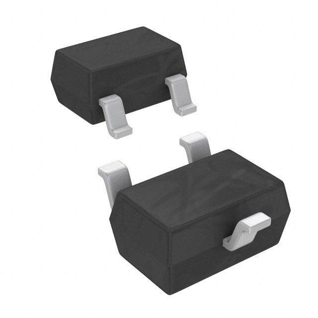
| 描述 | DIODE PIN ATTENUATOR 100V SOT-23PIN 二极管 100 VBR 0.35 pF |
| 产品分类 | RF 二极管分离式半导体 |
| 品牌 | Avago Technologies US Inc. |
| 产品手册 | http://www.avagotech.com/search/results.jsp?src=&siteCriteria=HSMP3814 |
| 产品图片 |
|
| rohs | 符合RoHS无铅 / 符合限制有害物质指令(RoHS)规范要求 |
| 产品系列 | 二极管与整流器,PIN 二极管,Avago Technologies HSMP-3814-TR1G- |
| 数据手册 | http://www.avagotech.com/docs/AV02-0402EN |
| 产品型号 | HSMP-3814-TR1G |
| 不同 If、F时的电阻 | 3 欧姆 @ 100mA,100MHz |
| 不同 Vr、F时的电容 | 0.35pF @ 50V,1MHz |
| 二极管类型 | PIN - 1 对共阴极 |
| 产品目录绘图 |
|
| 产品目录页面 | |
| 产品种类 | PIN 二极管 |
| 供应商器件封装 | SOT-23-3 |
| 其它名称 | 516-1800-2 |
| 功率耗散(最大值) | - |
| 包装 | 带卷 (TR) |
| 反向电压 | 50 V |
| 商标 | Avago Technologies |
| 安装风格 | SMD/SMT |
| 封装 | Reel |
| 封装/外壳 | TO-236-3,SC-59,SOT-23-3 |
| 封装/箱体 | SOT-23 |
| 工厂包装数量 | 3000 |
| 恢复时间 | 300 ns |
| 最大串联电阻(中频最大时) | 3 Ohms at 100 mA |
| 最大串联电阻(中频最小时) | 53 Ohms at 1 mA |
| 最大二极管电容 | 0.35 pF at 50 V |
| 最大工作温度 | + 150 C |
| 最小工作温度 | - 65 C |
| 标准包装 | 3,000 |
| 正向电流 | 1 A |
| 电压-峰值反向(最大值) | 100V |
| 电流-最大值 | 1A |
| 类型 | Attenuator |
| 载流子寿命 | 1.5 us |
| 配置 | Common Anode |


- 商务部:美国ITC正式对集成电路等产品启动337调查
- 曝三星4nm工艺存在良率问题 高通将骁龙8 Gen1或转产台积电
- 太阳诱电将投资9.5亿元在常州建新厂生产MLCC 预计2023年完工
- 英特尔发布欧洲新工厂建设计划 深化IDM 2.0 战略
- 台积电先进制程称霸业界 有大客户加持明年业绩稳了
- 达到5530亿美元!SIA预计今年全球半导体销售额将创下新高
- 英特尔拟将自动驾驶子公司Mobileye上市 估值或超500亿美元
- 三星加码芯片和SET,合并消费电子和移动部门,撤换高东真等 CEO
- 三星电子宣布重大人事变动 还合并消费电子和移动部门
- 海关总署:前11个月进口集成电路产品价值2.52万亿元 增长14.8%

PDF Datasheet 数据手册内容提取
HSMP-381x, 481x Surface Mount RF PIN Low Distortion Attenuator Diodes Data Sheet Description/Applications Features The HSMP-381x series is specifically designed for low dis- (cid:2) Diodes Optimized for: tortion attenuator applications. The HSMP-481x products – Low Distortion Attenuating feature ultra low parasitic inductance in the SOT-23 and – Microwave Frequency Operation SOT-323 packages. They are specifically designed for use (cid:2) Surface Mount Packages at frequencies which are much higher than the upper limit – Single and Dual Versions for conventional diodes. – Tape and Reel Options Available A SPICE model is not available for PIN diodes as SPICE (cid:2) Low Failure in Time (FIT) Rate[1] does not provide for a key PIN diode characteristic, carrier lifetime. (cid:2) Lead free Note: 1. For more information see the Surface Mount PIN Reliability Data Sheet. Package Lead Code Identification, Package Lead Code Identification, SOT-23 SOT-323 (Top View) (Top View) SINGLE SERIES SINGLE SERIES 3 3 1 2 1 2 #0 #2 B C COMMON COMMON COMMON COMMON ANODE CATHODE ANODE CATHODE 3 3 1 2 1 2 #3 #4 E F REVERSE DUAL SERIES CATHODE DUAL CATHODE 3 3 1 2 1 2 #5 4810 481B
Absolute Maximum Ratings[1] T = +25°C C Symbol Parameter Unit SOT-23 SOT-323 I Forward Current (1 μs Pulse) Amp 1 1 f P Peak Inverse Voltage V Same as V Same as V IV BR BR T Junction Temperature °C 150 150 j T Storage Temperature °C -65 to 150 -65 to 150 stg (cid:3) Thermal Resistance [2] °C/W 500 150 jc Notes: 1. Operation in excess of any one of these conditions may result in permanent damage to the device. 2. T = +25°C, where T is defined to be the temperature at the package pins where contact is made to the circuit board. C C Electrical Specifications T = +25°C (Each Diode) C Conventional Diodes Minimum Maximum Maximum Minimum Maximum Resistance Resistance Resistance Resistance Part Package Breakdown Total at at at at Number Marking Lead Voltage V Capacitance I = 0.01mA, I = 20mA, I = 100mA, I = 1mA, BR F F F F HSMP- Code Code Configuration (V) C (pF) RH (Ω) R (Ω) RT (Ω) R (Ω) T L M 3810 E0 0 Single 3812 E2 2 Series 3813 E3 3 Common Anode 3814 E4 4 Common Cathode 3815 E5 5 Reverse Series 100 0.35 1500 10 3.0 48 to 70 381B E0 B Single 381C E2 C Series 381E E3 E Common Anode 381F E4 F Common Cathode Test Conditions V = V V = 50V I = 0.01mA I = 20mA I = 100mA I = 1mA R BR R F F F F Measure f = 1MHz f = 100MHz f = 100MHz f = 100MHz f = 100MHz I≤ 10uA R High Frequency (Low Inductance, 500 MHz – 3 GHz) PIN Diodes Minimum Maximum Series Typical Maximum Typical Part Package Breakdown Series Resistance Total Total Total Number Marking Lead Voltage Resistance I = 1mA, Capacitance Capacitance Inductance F HSMP- Code Code Configuration V (V) R (Ω) R (Ω) C (pF) C (pF) L (nH) BR S M T T T 4810 EB B Dual Cathode 100 3 48 - 70 0.35 0.4 1 481B EB B Dual Cathode Test Conditions V = V I = 100mA I = 1mA V = 50V V = 50V f = R BR F F R R Measure f = f = 100MHz f = 1MHz f = 1MHz 500MHz I ≤ 10μA 100MHz - 3GHz R 2
Typical Parameters at T = 25°C C Total Part Number Series Resistance Carrier Lifetime Reverse Recovery Time Capacitance HSMP- R (Ω) (cid:4) (ns) T (ns) C (pF) S rr T 381x 53 1500 300 0.27 @ 50 V Test Conditions I = 1 mA I = 50 mA V = 10 V f = 1 MHz F F R f = 100 MHz I = 250 mA I = 20 mA R F 90% Recovery Typical Parameters at T = 25°C (unless otherwise noted), Single Diode C 0.45 10000 120 Diode Mounted as a CITANCE (pF) 000...334050 1 MHz NCE (OHMS)1010000 TTTAAA === ++–825555 CCC EPT POINT (dBm) 1110980000 Sianne adri e5Ts0e sAOttehtdemn a uMt a1itc2or3ro MstHrizp A A C P T R A S E 70 TOTAL C 00..2250 3fr0e qMuHezncy>100 MHz RF RESI 10 NPUT INT 6500 I 0.15 1 40 0 2 4 6 8 10 12 14 16 18 20 0.01 0.1 1 10 100 1000 100 10 REVERSE VOLTAGE (V) IF – FORWARD BIAS CURRENT (mA) DIODE RF RESISTANCE (OHMS) Figure 1. RF Capacitance vs. Reverse Figure 2. RF Resistance vs. Forward Figure 3. 2nd Harmonic Input Bias. Bias Current, f = 100MHz Intercept Point vs. Diode RF Resistance. 100 Typical Applications for Multiple Diode Products A) m T ( 10 VARIABLE BIAS N E R R U C D 1 R A W OR 0.1 INPUT RF IN/OUT F – F I 125 C 25 C –50 C 0.01 0 0.2 0.4 0.6 0.8 1.0 1.2 VF – FORWARD VOLTAGE (mA) Figure 4. Forward Current vs. Forward Voltage. FIXED BIAS VOLTAGE Figure 5. Four Diode π Attenuator. See Application Note 1048 for Details. Notes: 3. Typical values were derived using limited samples during initial product characterization and may not be representative of the overall distribution. 3
Typical Applications for HSMP-481x Low Inductance Series Microstrip Series Connection for HSMP-481x Series In order to take full advantage of the low inductance of the HSMP-481x series when using them in series applications, both lead 1 and lead 2 should be connected together, as shown in Figure 7. 3 1 2 HSMP-481x Figure 6. Internal Connections. Figure 7. Circuit Layout. Microstrip Shunt Connections for HSMP-481x Series In Figure 8, the center conductor of the microstrip line is interrupted and leads 1 and 2 of the HSMP-481x series diode are placed across the resulting gap. This forces the 1.5 nH lead inductance of leads 1 and 2 to appear as part of a low pass filter, reducing the shunt parasitic inductance and increasing the maximum available attenuation. The 0.3 nHof shunt inductance external to the diode is created by the via holes, and is a good estimate for 0.032" thick material. 1.5 nH 1.5 nH 50 OHM MICROSTRIP LINES Rj 0.3 pF 0.3 nH 0.08 PAD CONNECTED TO Rj Ib0.9+ 2.5 0.3 nH GROUND BY TWO VIA HOLES Figure 8. Circuit Layout. Figure 9. Equivalent Circuit. 4
Typical Applications for HSMP-481x Low Inductance Series (continued) Co-Planar Waveguide Shunt Connection for HSMP-481x Equivalent Circuit Model Series HSMP-381x Chip* Co-Planar waveguide, with ground on the top side of the printed circuit board, is shown in Figure 10. Since it elimi- Rs Rj nates the need for via holes to ground, it offers lower shunt parasitic inductance and higher maximum attenuation 2.5 Ω when compared to microstrip circuit. Cj RT = 2.5 + Rj Co-Planar Waveguide CT = CP + Cj 0.18 pF* Groundplane 80 * Measured at -20 V Center Conductor Rj = I0.9 Ω Groundplane I = Forward Bias Current in mA *See AN1124 for package models. Figure 10. Circuit Layout. Rj 0.3 pF 0.75 nH Figure 11. Equivalent Circuit. 5
Assembly Information SMT Assembly SOT-323 PCB Footprint Reliable assembly of surface mount components is a A recommended PCB pad layout for the miniature SOT-323 complex process that involves many material, process, and (SC-70) package is shown in Figure 12 (dimensions are in equipment factors, including: method of heating (e.g., IR inches). This layout provides ample allowance for package or vapor phase reflow, wave soldering, etc.) circuit board placement by automated assembly equipment without material, conductor thickness and pattern, type of solder adding parasitics that could impair the performance. alloy, and the thermal conductivity and thermal mass of components. Components with a low mass, such as the SOT-323/-23 package, will reach solder reflow tempera- 0.026 tures faster than those with a greater mass. After ramping up from room temperature, the circuit board with components attached to it (held in place with solder 0.079 paste) passes through one or more preheat zones. The preheat zones increase the temperature of the board and 0.039 components to prevent thermal shock and begin evaporat- ing solvents from the solder paste. The reflow zone briefly 0.022 elevates the temperature sufficiently to produce a reflow of the solder. Dimensions in inches Figure 12. Recommended PCB Pad Layout The rates of change of temperature for the ramp-up and for Avago’s SC70 3L/SOT-323 Products. cool-down zones are chosen to be low enough to not cause deformation of the board or damage to components SOT-23 PCB Footprint due to thermal shock. The maximum temperature in the 0.039 reflow zone (T ) should not exceed 260°C. 0.039 1 MAX 1 These parameters are typical for a surface mount assembly process for Avago diodes. As a general guideline, the circuit board and components should be exposed only to the 0.079 minimum temperatures and times necessary to achieve a 2.0 uniform reflow of solder. 0.035 0.9 0.031 0.8 inches Dimensions in mm Figure 13. Recommended PCB Pad Layout for Avago’s SOT-23 Products. 6
Package Dimensions Outline 23 (SOT-23) Outline SOT-323 (SC-70) e2 e1 e1 E XXX E1 E XXX E1 e L e L B C D DIMENSIONS (mm) B C SYMBOL MIN. MAX. A 0.80 1.00 D DIMENSIONS (mm) A A1 0.00 0.10 SYMBOL MIN. MAX. B 0.15 0.40 A 0.79 1.20 C 0.08 0.25 A1 0.000 0.100 A1 D 1.80 2.25 A B 0.30 0.54 E1 1.10 1.40 C 0.08 0.20 e 0.65 typical A1 D 2.73 3.13 Notes: e1 1.30 typical E1 1.15 1.50 XXX-package marking E 1.80 2.40 e 0.89 1.02 Drawings are not to scale L 0.26 0.46 e1 1.78 2.04 Notes: e2 0.45 0.60 XXX-package marking E 2.10 2.70 Drawings are not to scale L 0.45 0.69 Package Characteristics Lead Material ....................................................Copper (SOT-323); Alloy 42 (SOT-23) Lead Finish .........................................................................Tin 100% (Lead-free option) Maximum Soldering Temperature ............................................260°C for 5 seconds Minimum Lead Strength ...........................................................................2 pounds pull Typical Package Inductance ......................................................................................2 nH Typical Package Capacitance ..............................................0.08 pF (opposite leads) Ordering Information Specify part number followed by option. For example: HSMP - 381x - XXX Bulk or Tape and Reel Option Part Number; x = Lead Code Surface Mount PIN Option Descriptions -BLKG = Bulk, 100 pcs. per antistatic bag -TR1G = Tape and Reel, 3000 devices per 7" reel -TR2G = Tape and Reel, 10,000 devices per 13" reel Tape and Reeling conforms to Electronic Industries RS-481, “Taping of Surface Mounted Components for Automated Placement.” 7
Device Orientation For Outlines SOT-23/323 TOP VIEW END VIEW REEL 4 mm 8 mm ABC ABC ABC ABC CARRIER TAPE USER Note: "AB" represents package marking code. FEED "C" represents date code. DIRECTION COVER TAPE Tape Dimensions and Product Orientation For Outline SOT-23 P D P2 E P0 F W t1 D1 9(cid:1) MAX Ko 8(cid:1) MAX 13.5(cid:1) MAX A0 B0 DESCRIPTION SYMBOL SIZE (mm) SIZE (INCHES) CAVITY LENGTH A0 3.15 ± 0.10 0.124 ± 0.004 WIDTH B0 2.77 ± 0.10 0.109 ± 0.004 DEPTH K0 1.22 ± 0.10 0.048 ± 0.004 PITCH P 4.00 ± 0.10 0.157 ± 0.004 BOTTOM HOLE DIAMETER D1 1.00 + 0.05 0.039 ± 0.002 PERFORATION DIAMETER D 1.50 + 0.10 0.059 + 0.004 PITCH P0 4.00 ± 0.10 0.157 ± 0.004 POSITION E 1.75 ± 0.10 0.069 ± 0.004 CARRIER TAPE WIDTH W 8.00 + 0.30 - 0.10 0.315 + 0.012 - 0.004 THICKNESS t1 0.229 ± 0.013 0.009 ± 0.0005 DISTANCE CAVITY TO PERFORATION F 3.50 ± 0.05 0.138 ± 0.002 BETWEEN (WIDTH DIRECTION) CENTERLINE CAVITY TO PERFORATION P2 2.00 ± 0.05 0.079 ± 0.002 (LENGTH DIRECTION) 8
Tape Dimensions and Product Orientation For Outline SOT-323 P D P2 P0 E F W C D1 t1 (CARRIER TAPE THICKNESS) Tt (COVER TAPE THICKNESS) An K0 An A0 B0 DESCRIPTION SYMBOL SIZE (mm) SIZE (INCHES) CAVITY LENGTH A0 2.40 ±(cid:1) 0.10 0.094 ±(cid:1) 0.004 WIDTH B0 2.40 ±(cid:1) 0.10 0.094 ±(cid:1) 0.004 DEPTH K0 1.20 ±(cid:1) 0.10 0.047 ±(cid:1) 0.004 PITCH P 4.00 ±(cid:1) 0.10 0.157 ±(cid:1) 0.004 BOTTOM HOLE DIAMETER D1 1.00 + 0.25 0.039 + 0.010 PERFORATION DIAMETER D 1.55 ±(cid:1) 0.05 0.061 ±(cid:1) 0.002 PITCH P0 4.00 ±(cid:1) 0.10 0.157 ±(cid:1) 0.004 POSITION E 1.75 ±(cid:1) 0.10 0.069 ±(cid:1) 0.004 CARRIER TAPE WIDTH W 8.00 ±(cid:1) 0.30 0.315 ±(cid:1) 0.012 THICKNESS t1 0.254 ±(cid:1) 0.02 0.0100 ±(cid:1) 0.0008 COVER TAPE WIDTH C 5.4 ±(cid:1) 0.10 0.205 ±(cid:1) 0.004 TAPE THICKNESS Tt 0.062 ±(cid:1) 0.001 0.0025 ±(cid:1) 0.00004 DISTANCE CAVITY TO PERFORATION F 3.50 ±(cid:1) 0.05 0.138 ±(cid:1) 0.002 (WIDTH DIRECTION) CAVITY TO PERFORATION P2 2.00 ±(cid:1) 0.05 0.079 ±(cid:1) 0.002 (LENGTH DIRECTION) ANGLE FOR SOT-323 (SC70-3 LEAD) An 8(cid:1)C MAX FOR SOT-363 (SC70-6 LEAD) 10(cid:1)C MAX For product information and a complete list of distributors, please go to our web site: www.avagotech.com Avago, Avago Technologies, and the A logo are trademarks of Avago Technologies in the United States and other countries. Data subject to change. Copyright © 2005-2009 Avago Technologies. All rights reserved. Obsoletes AV01-0378EN AV02-0402EN - December 22, 2009