ICGOO在线商城 > 集成电路(IC) > 时钟/计时 - 时钟发生器,PLL,频率合成器 > HEF4046BT,653

 Datasheet下载
- 型号: HEF4046BT,653
- 制造商: NXP Semiconductors
- 库位|库存: xxxx|xxxx
- 要求:
| 数量阶梯 | 香港交货 | 国内含税 |
| +xxxx | $xxxx | ¥xxxx |
查看当月历史价格
查看今年历史价格
HEF4046BT,653产品简介:
ICGOO电子元器件商城为您提供HEF4046BT,653由NXP Semiconductors设计生产,在icgoo商城现货销售,并且可以通过原厂、代理商等渠道进行代购。 HEF4046BT,653价格参考。NXP SemiconductorsHEF4046BT,653封装/规格:时钟/计时 - 时钟发生器,PLL,频率合成器, 。您可以下载HEF4046BT,653参考资料、Datasheet数据手册功能说明书,资料中有HEF4046BT,653 详细功能的应用电路图电压和使用方法及教程。
HEF4046BT 是 Nexperia USA Inc. 生产的一款时钟/计时器件,属于时钟发生器、PLL(锁相环)和频率合成器类别。该型号的应用场景主要集中在需要信号生成、频率转换和同步的电子系统中。以下是其主要应用场景及功能描述:

1. 振荡器和信号生成
   HEF4046BT 可用作振荡器的核心组件,用于生成稳定的时钟信号。它适用于需要精确频率控制的场景,例如音频设备、通信模块或测试仪器中的信号源。

2. 频率合成与倍频/分频
   该芯片支持频率合成功能,能够通过 PLL 技术实现输入信号的倍频或分频操作。这使其适合应用于无线通信系统、射频电路以及数字信号处理设备中,用于生成所需的载波或本地振荡信号。

3. 时钟恢复与同步
   在数据传输系统中,HEF4046BT 可用于从输入信号中提取时钟信息,并将其与其他系统组件同步。这种能力在光纤通信、以太网或其他高速数据链路中尤为重要。

4. 消费电子产品中的应用
   HEF4046BT 的小型化设计和低功耗特性使其成为消费电子产品的理想选择,如电视、音响设备、家用自动化控制器等。它可以为这些设备提供稳定的时钟信号,确保系统的正常运行。

5. 工业控制与测量设备
   在工业领域,该芯片可用于精密测量仪器、电机控制单元或自动化系统中,为传感器接口、数据采集模块和其他子系统提供可靠的时钟信号。

6. 汽车电子系统
   HEF4046BT 还可应用于汽车电子领域,例如车载娱乐系统、导航设备或发动机控制单元(ECU)。它能够满足汽车环境中对稳定性和可靠性的严格要求。

综上所述,HEF4046BT 的应用场景涵盖了通信、消费电子、工业控制和汽车电子等多个领域。其核心优势在于提供高精度的时钟信号、灵活的频率转换能力和良好的稳定性,能够满足多样化的设计需求。
| 参数 | 数值 |
| 产品目录 | 集成电路 (IC)半导体 |
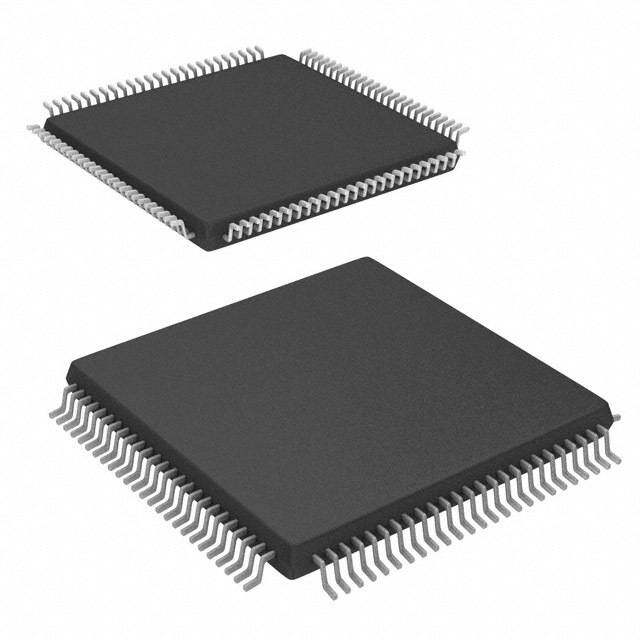
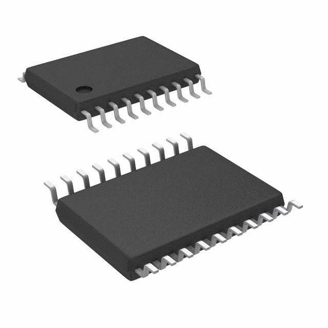
| 描述 | IC PHASE LOCK LOOP W/VCO 16SOIC锁相环 - PLL PHASE LOCKED LOOP |
| 产品分类 | |
| 品牌 | NXP Semiconductors |
| 产品手册 | |
| 产品图片 |
|
| rohs | 符合RoHS无铅 / 符合限制有害物质指令(RoHS)规范要求 |
| 产品系列 | RF集成电路,锁相环 - PLL,NXP Semiconductors HEF4046BT,653HE4000B |
| 数据手册 | |
| 产品型号 | HEF4046BT,653 |
| PCN封装 | |
| PCN组件/产地 | |
| PLL | 是 |
| 产品种类 | 锁相环 - PLL |
| 供应商器件封装 | 16-SO |
| 其它名称 | 568-8231-1 |
| 分频器/倍频器 | 无/无 |
| 包装 | 剪切带 (CT) |
| 商标 | NXP Semiconductors |
| 安装类型 | 表面贴装 |
| 安装风格 | SMD/SMT |
| 封装 | Reel |
| 封装/外壳 | 16-SOIC(0.154",3.90mm 宽) |
| 封装/箱体 | SO-16 |
| 工作温度 | -40°C ~ 85°C |
| 工作电源电压 | 3.3 V, 5 V, 9 V, 12 V |
| 工厂包装数量 | 2500 |
| 差分-输入:输出 | 无/无 |
| 最大工作温度 | + 85 C |
| 最小工作温度 | - 40 C |
| 标准包装 | 1 |
| 比率-输入:输出 | 1:4 |
| 电压-电源 | 3 V ~ 15 V |
| 电源电压-最大 | 15 V |
| 电源电压-最小 | 3 V |
| 电路数 | 1 |
| 电路数量 | 1 |
| 类型 | PLL |
| 输入 | 时钟 |
| 输出 | 时钟 |
| 零件号别名 | HEF4046BTD-T |
| 频率-最大值 | 2.7MHz |


- 商务部:美国ITC正式对集成电路等产品启动337调查
- 曝三星4nm工艺存在良率问题 高通将骁龙8 Gen1或转产台积电
- 太阳诱电将投资9.5亿元在常州建新厂生产MLCC 预计2023年完工
- 英特尔发布欧洲新工厂建设计划 深化IDM 2.0 战略
- 台积电先进制程称霸业界 有大客户加持明年业绩稳了
- 达到5530亿美元!SIA预计今年全球半导体销售额将创下新高
- 英特尔拟将自动驾驶子公司Mobileye上市 估值或超500亿美元
- 三星加码芯片和SET,合并消费电子和移动部门,撤换高东真等 CEO
- 三星电子宣布重大人事变动 还合并消费电子和移动部门
- 海关总署:前11个月进口集成电路产品价值2.52万亿元 增长14.8%


PDF Datasheet 数据手册内容提取
HEF4046B Phase-locked loop Rev. 6 — 24 March 2016 Product data sheet 1. General description The HEF4046B is a phase-locked loop circuit that consists of a linear Voltage Controlled Oscillator (VCO) and two different phase comparators with a common signal input amplifier and a common comparator input. A 7V regulator (Zener) diode is provided for supply voltage regulation if necessary. For a functional description see Section6. It operates over a recommended V power supply range of 3V to 15V referenced to V DD SS (usually ground). Unused inputs must be connected to V , V , or another input. DD SS 2. Features and benefits Fully static operation 5 V, 10 V, and 15 V parametric ratings Standardized symmetrical output characteristics Specified from 40 C to +85 C Complies with JEDEC standard JESD 13-B 3. Ordering information Table 1. Ordering info rmation All types operate from 40C to +85C. Type number Package Name Description Version HEF4046BT SO16 plastic small outline package; 16 leads; body width 3.9mm SOT109-1
HEF4046B Nexperia Phase-locked loop 4. Functional diagram (cid:51)(cid:43)(cid:36)(cid:54)(cid:40)(cid:3) (cid:38)(cid:50)(cid:48)(cid:51)(cid:36)(cid:53)(cid:36)(cid:55)(cid:50)(cid:53)(cid:3)(cid:20) (cid:20)(cid:23) (cid:54)(cid:44)(cid:42)(cid:66)(cid:44)(cid:49) (cid:21) (cid:51)(cid:38)(cid:20)(cid:66)(cid:50)(cid:56)(cid:55) (cid:38)(cid:50)(cid:48)(cid:3) (cid:51)(cid:66)(cid:44)(cid:49) (cid:22) (cid:20)(cid:22) (cid:51)(cid:38)(cid:21)(cid:66)(cid:50)(cid:56)(cid:55) (cid:51)(cid:43)(cid:36)(cid:54)(cid:40)(cid:3) (cid:53)(cid:22) (cid:183)(cid:3)(cid:49) (cid:38)(cid:50)(cid:48)(cid:51)(cid:36)(cid:53)(cid:36)(cid:55)(cid:50)(cid:53)(cid:3)(cid:21) (cid:20) (cid:51)(cid:38)(cid:51) (cid:57)(cid:38)(cid:50)(cid:66)(cid:50)(cid:56)(cid:55) (cid:23) (cid:28) (cid:57)(cid:38)(cid:50)(cid:66)(cid:44)(cid:49) (cid:47)(cid:50)(cid:58)(cid:16)(cid:51)(cid:36)(cid:54)(cid:54)(cid:3) (cid:41)(cid:44)(cid:47)(cid:55)(cid:40)(cid:53) (cid:38)(cid:20)(cid:36) (cid:25) (cid:38)(cid:21) (cid:38)(cid:20) (cid:38)(cid:20)(cid:37) (cid:26) (cid:54)(cid:50)(cid:56)(cid:53)(cid:38)(cid:40)(cid:3) (cid:20)(cid:19) (cid:54)(cid:41)(cid:66)(cid:50)(cid:56)(cid:55) (cid:57)(cid:38)(cid:50) (cid:41)(cid:50)(cid:47)(cid:47)(cid:50)(cid:58)(cid:40)(cid:53) (cid:57)(cid:54)(cid:54) (cid:53)(cid:20) (cid:53)(cid:20) (cid:20)(cid:20) (cid:53)(cid:54)(cid:41) (cid:57)(cid:54)(cid:54) (cid:53)(cid:21) (cid:53)(cid:21) (cid:20)(cid:21) (cid:57)(cid:54)(cid:54) (cid:24) (cid:44)(cid:49)(cid:43) (cid:57)(cid:54)(cid:54)(cid:3) (cid:20)(cid:24) (cid:61)(cid:40)(cid:49)(cid:40)(cid:53) (cid:11)(cid:83)(cid:76)(cid:81)(cid:3)(cid:27)(cid:12) (cid:19)(cid:19)(cid:20)(cid:68)(cid:68)(cid:72)(cid:25)(cid:21)(cid:25) Fig 1. Functional diagram 5. Pinning information 5.1 Pinning (cid:43)(cid:40)(cid:41)(cid:23)(cid:19)(cid:23)(cid:25)(cid:37) (cid:51)(cid:38)(cid:51)(cid:66)(cid:50)(cid:56)(cid:55) (cid:20) (cid:20)(cid:25) (cid:57)(cid:39)(cid:39) (cid:51)(cid:38)(cid:20)(cid:66)(cid:50)(cid:56)(cid:55) (cid:21) (cid:20)(cid:24) (cid:61)(cid:40)(cid:49)(cid:40)(cid:53) (cid:38)(cid:50)(cid:48)(cid:51)(cid:66)(cid:44)(cid:49) (cid:22) (cid:20)(cid:23) (cid:54)(cid:44)(cid:42)(cid:66)(cid:44)(cid:49) (cid:57)(cid:38)(cid:50)(cid:66)(cid:50)(cid:56)(cid:55) (cid:23) (cid:20)(cid:22) (cid:51)(cid:38)(cid:21)(cid:66)(cid:50)(cid:56)(cid:55) (cid:44)(cid:49)(cid:43) (cid:24) (cid:20)(cid:21) (cid:53)(cid:21) (cid:38)(cid:20)(cid:36) (cid:25) (cid:20)(cid:20) (cid:53)(cid:20) (cid:38)(cid:20)(cid:37) (cid:26) (cid:20)(cid:19) (cid:54)(cid:41)(cid:66)(cid:50)(cid:56)(cid:55) (cid:57)(cid:54)(cid:54) (cid:27) (cid:28) (cid:57)(cid:38)(cid:50)(cid:66)(cid:44)(cid:49) (cid:19)(cid:19)(cid:20)(cid:68)(cid:68)(cid:72)(cid:25)(cid:21)(cid:26) Fig 2. Pin configuration HEF4046B All information provided in this document is subject to legal disclaimers. © Nexperia B.V. 2017. All rights reserved Product data sheet Rev. 6 — 24 March 2016 2 of 19
HEF4046B Nexperia Phase-locked loop 5.2 Pin description Table 2. Pin descripti on Symbol Pin Description PCP_OUT 1 phase comparator pulse output PC1_OUT 2 phase comparator 1 output COMP_IN 3 comparator input VCO_OUT 4 VCO output INH 5 inhibit input C1A 6 capacitor C1 connection A C1B 7 capacitor C1 connection B V 8 ground supply voltage SS VCO_IN 9 VCO input SF_OUT 10 source-follower output R1 11 resistor R1 connection R2 12 resistor R2 connection PC2_OUT 13 phase comparator 2 output SIG_IN 14 signal input ZENER 15 Zener diode input for regulated supply V 16 supply voltage DD 6. Functional description 6.1 VCO control The VCO requires an external capacitor (C1) and resistor (R1) with an optional resistor (R2). Resistor R1 and capacitor C1 determine the frequency range of the VCO, while resistor R2 enables the VCO to have a frequency off-set if required. The high input impedance of the VCO simplifies the design of low-pass filters; it permits the designer a wide choice of resistor/capacitor ranges. In order not to load the low-pass filter, a source-follower output of the VCO input voltage is provided at SF_OUT (pin 10). If this is used, a load resistor (R ) should be connected from SF_OUT to V ; if unused, SF_OUT L SS should be left open. The VCO output (pin 4) can either be connected directly to the comparator input COMP_IN (pin 3) or via a frequency divider. A LOW-level at the inhibit input INH_IN (pin 5) enables the VCO and the source follower, while a HIGH-level turns both off to minimize standby power consumption. 6.2 Phase comparators The phase-comparator signal input SIG_IN (pin 14) can be direct-coupled, provided the signal swing is between the standard HE4000B family input logic levels. The signal must be capacitively coupled to the self-biasing amplifier at the signal input with smaller swings. Phase comparator 1 is an EXCLUSIVE-OR network. The signal and comparator input frequencies must have a 50 % duty factor to obtain the maximum lock range. The average output voltage of the phase comparator is equal to 0.5V when there is no signal or noise DD at the signal input. The average voltage to the VCO input VCO_IN is supplied by the low-pass filter connected to the output of phase comparator 1. This also causes the VCO to oscillate at the center frequency (f ). The frequency capture range (2f ) is defined as 0 C HEF4046B All information provided in this document is subject to legal disclaimers. © Nexperia B.V. 2017. All rights reserved Product data sheet Rev. 6 — 24 March 2016 3 of 19
HEF4046B Nexperia Phase-locked loop the frequency range of input signals on which the PLL will lock if it was initially out of lock. The frequency lock range (2f ) is defined as the frequency range of input signals on which L the loop will stay locked if it was initially in lock. The capture range is smaller or equal to the lock range. With phase comparator 1, the range of frequencies over which the PLL can acquire lock (capture range) depends on the low-pass filter characteristics and this range can be made as large as the lock range. Phase comparator 1 enables the PLL system to remain in lock in spite of high amounts of noise in the input signal. A typical behavior of this type of phase comparator is that it may lock onto input frequencies that are close to harmonics of the VCO center frequency. Another typical behavior is that the phase angle between the signal and comparator input varies between 0 and 180, and is 90at the center frequency. Figure3 shows the typical phase-to-output response characteristic. Figure4 shows the typical waveforms for a PLL with a f locked phase comparator 1. 0 (cid:57)(cid:39)(cid:39)(cid:11)(cid:20)(cid:12) (cid:19)(cid:17)(cid:24)(cid:57)(cid:39)(cid:39) (cid:19) (cid:19)(cid:131)(cid:3) (cid:28)(cid:19)(cid:131)(cid:3) (cid:20)(cid:27)(cid:19)(cid:131)(cid:3) (cid:19)(cid:19)(cid:20)(cid:68)(cid:68)(cid:72)(cid:25)(cid:21)(cid:27) (1) Average output voltage. Fig 3. Signal-to-comparator inputs phase difference for comparator 1 (cid:54)(cid:44)(cid:42)(cid:66)(cid:44)(cid:49) (cid:38)(cid:50)(cid:48)(cid:51)(cid:66)(cid:44)(cid:49)(cid:3) (cid:57)(cid:38)(cid:50)(cid:66)(cid:50)(cid:56)(cid:55)(cid:3) (cid:3) (cid:3) (cid:51)(cid:38)(cid:20)(cid:66)(cid:50)(cid:56)(cid:55) (cid:57)(cid:39)(cid:39) (cid:57)(cid:38)(cid:50)(cid:66)(cid:44)(cid:49) (cid:57)(cid:54)(cid:54) (cid:19)(cid:19)(cid:20)(cid:68)(cid:68)(cid:72)(cid:25)(cid:21)(cid:28) Fig 4. Typical waveforms for phase-locked loop with a f locked phase comparator 1 0 HEF4046B All information provided in this document is subject to legal disclaimers. © Nexperia B.V. 2017. All rights reserved Product data sheet Rev. 6 — 24 March 2016 4 of 19
HEF4046B Nexperia Phase-locked loop Phase comparator 2 is an edge-controlled digital memory network. It consists of four flip-flops, control gating and a 3-state output circuit comprising p and n-type drivers with a common output node. When the p-type or n-type drivers are ON, they pull the output up to V or down to V respectively. This type of phase comparator only acts on the DD SS positive-going edges of the signals at SIG_INand COMP_IN. Therefore, the duty factors of these signals are not of importance. If the signal input frequency is higher than the comparator input frequency, the p-type output driver is maintained ON most of the time, and both the n and p-type drivers are OFF (3-state) the remainder of the time. If the signal input frequency is lower than the comparator input frequency, the n-type output driver is maintained ON most of the time, and both the n and p-type drivers are OFF the remainder of the time. If the signal input and comparator input frequencies are equal, but the signal input lags the comparator input in phase, the n-type output driver is maintained ON for a time corresponding to the phase difference. If the comparator input lags the signal input in phase, the p-type output driver is maintained ON for a time corresponding to the phase difference. Subsequently, the voltage at the capacitor of the low-pass filter connected to this phase comparator is adjusted until the signal and comparator inputs are equal in both phase and frequency. At this stable point, both p and n-type drivers remain OFF and thus the phase comparator output becomes an open circuit and keeps the voltage at the capacitor of the low-pass filter constant. Moreover, the signal at the phase comparator pulse output (PCP_OUT) is a HIGH level, which can be used for indicating a locked condition. Thus, for phase comparator 2, no phase difference exists between the signal and comparator inputs over the full VCO frequency range. Moreover, the power dissipation due to the low-pass filter is reduced when this type of phase comparator is used, because both p and n-type output drivers are OFF for most of the signal input cycle. It should be noted that the PLL lock range for this type of phase comparator is equal to the capture range, independent of the low-pass filter. With no signal present at the signal input, the VCO is adjusted to its lowest frequency for phase comparator 2. Figure5 shows typical waveforms for a PLL employing this type of locked phase comparator. (cid:54)(cid:44)(cid:42)(cid:66)(cid:44)(cid:49) (cid:38)(cid:50)(cid:48)(cid:51)(cid:66)(cid:44)(cid:49)(cid:3) (cid:57)(cid:38)(cid:50)(cid:66)(cid:50)(cid:56)(cid:55)(cid:3) (cid:3) (cid:3) (cid:57)(cid:39)(cid:39) (cid:51)(cid:38)(cid:21)(cid:66)(cid:50)(cid:56)(cid:55) (cid:75)(cid:76)(cid:74)(cid:75)(cid:3)(cid:76)(cid:80)(cid:83)(cid:72)(cid:71)(cid:68)(cid:81)(cid:70)(cid:72)(cid:3)(cid:50)(cid:41)(cid:41)(cid:16)(cid:86)(cid:87)(cid:68)(cid:87)(cid:72) (cid:57)(cid:54)(cid:54) (cid:57)(cid:38)(cid:50)(cid:66)(cid:44)(cid:49) (cid:51)(cid:38)(cid:51)(cid:66)(cid:50)(cid:56)(cid:55) (cid:19)(cid:19)(cid:20)(cid:68)(cid:68)(cid:72)(cid:25)(cid:22)(cid:19) Fig 5. Typical waveforms for phase-locked loop with a locked phase comparator 2 HEF4046B All information provided in this document is subject to legal disclaimers. © Nexperia B.V. 2017. All rights reserved Product data sheet Rev. 6 — 24 March 2016 5 of 19
HEF4046B Nexperia Phase-locked loop Figure6 shows the state diagram for phase comparator 2. Each circle represents a state of the comparator. The number at the top, inside each circle, represents the state of the comparator, while the logic state of the signal and comparator inputs are represented by a ‘0’ for a logic LOW or a ‘1’ for a logic HIGH, and they are shown in the left and right bottom of each circle. The transitions from one to another result from either a logic change at the signal input (S representing SIG_IN) or the comparator input (C representing COMP_IN). A positive- going and a negative-going transition are shown by an arrow pointing up or down respectively. The state diagram assumes, that only one transition on either the signal input or comparator input occurs at any instant. • States 3, 5, 9 and 11 represent the output condition when the p-type driver is ON. • States 2, 4, 10 and 12 determine the condition when the n-type driver is ON. • States 1, 6, 7 and 8 represent the condition when the output is in its high-impedance OFF state; i.e. both p and n-type drivers are OFF, and the PCP_OUToutput is HIGH. The condition at output PCP_OUT for all other states is LOW. (cid:20) (cid:19) (cid:19) (cid:38) (cid:54) (cid:54) (cid:38) (cid:54) (cid:38) (cid:23) (cid:21) (cid:22) (cid:24) (cid:19) (cid:19) (cid:19) (cid:20) (cid:20) (cid:19) (cid:19) (cid:19) (cid:38) (cid:54) (cid:54) (cid:38) (cid:54) (cid:38) (cid:27) (cid:38) (cid:25) (cid:54) (cid:26) (cid:20) (cid:19) (cid:20) (cid:20) (cid:19) (cid:20) (cid:54) (cid:54) (cid:38) (cid:38) (cid:38) (cid:54) (cid:38) (cid:54) (cid:20)(cid:19) (cid:20)(cid:21) (cid:20)(cid:20) (cid:28) (cid:20) (cid:20) (cid:20) (cid:19) (cid:19) (cid:20) (cid:20) (cid:20) (cid:38) (cid:54) (cid:81)(cid:16)(cid:87)(cid:92)(cid:83)(cid:72)(cid:3)(cid:71)(cid:85)(cid:76)(cid:89)(cid:72)(cid:85)(cid:3)(cid:50)(cid:49) (cid:83)(cid:16)(cid:87)(cid:92)(cid:83)(cid:72)(cid:3)(cid:71)(cid:85)(cid:76)(cid:89)(cid:72)(cid:85)(cid:3)(cid:50)(cid:49) (cid:86)(cid:87)(cid:68)(cid:87)(cid:72)(cid:3)(cid:81)(cid:88)(cid:80)(cid:69)(cid:72)(cid:85)(cid:3)(cid:82)(cid:73)(cid:3) (cid:87)(cid:75)(cid:72)(cid:3)(cid:70)(cid:82)(cid:80)(cid:83)(cid:68)(cid:85)(cid:68)(cid:87)(cid:82)(cid:85) (cid:81)(cid:3)(cid:68)(cid:81)(cid:71)(cid:3)(cid:83)(cid:16)(cid:87)(cid:92)(cid:83)(cid:72)(cid:3) (cid:81) (cid:71)(cid:85)(cid:76)(cid:89)(cid:72)(cid:85)(cid:86)(cid:3)(cid:68)(cid:85)(cid:72)(cid:3)(cid:50)(cid:41)(cid:41) (cid:19) (cid:19) (cid:79)(cid:82)(cid:74)(cid:76)(cid:70)(cid:3)(cid:86)(cid:87)(cid:68)(cid:87)(cid:72)(cid:3)(cid:82)(cid:73)(cid:3) (cid:70)(cid:82)(cid:80)(cid:83)(cid:68)(cid:85)(cid:68)(cid:87)(cid:82)(cid:85)(cid:3)(cid:76)(cid:81)(cid:83)(cid:88)(cid:87)(cid:3)(cid:11)(cid:83)(cid:76)(cid:81)(cid:3)(cid:22)(cid:12) (cid:19)(cid:19)(cid:20)(cid:68)(cid:68)(cid:72)(cid:25)(cid:22)(cid:20) (cid:79)(cid:82)(cid:74)(cid:76)(cid:70)(cid:3)(cid:86)(cid:87)(cid:68)(cid:87)(cid:72)(cid:3)(cid:82)(cid:73)(cid:3) (cid:86)(cid:76)(cid:74)(cid:81)(cid:68)(cid:79)(cid:3)(cid:76)(cid:81)(cid:83)(cid:88)(cid:87)(cid:3)(cid:11)(cid:83)(cid:76)(cid:81)(cid:3)(cid:20)(cid:23)(cid:12) S : 0 to 1 transition at the signal input SIG_IN. C : 1 to 0 transition at the comparator input COMP_IN. Fig 6. State diagram for comparator 2 HEF4046B All information provided in this document is subject to legal disclaimers. © Nexperia B.V. 2017. All rights reserved Product data sheet Rev. 6 — 24 March 2016 6 of 19
HEF4046B Nexperia Phase-locked loop 7. Limiting values Table 3. Limiting valu es In accordance with the Absolute Maximum Rating System (IEC 60134). Symbol Parameter Conditions Min Max Unit V supply voltage 0.5 +18 V DD I input clamping current V <0.5V or V >V + 0.5 V - 10 mA IK I I DD V input voltage 0.5 V + 0.5 V I DD I output clamping current V <0.5V or V >V + 0.5 V - 10 mA OK O O DD I input/output current - 10 mA I/O I supply current - 50 mA DD T storage temperature 65 +150 C stg T ambient temperature 40 +85 C amb P total power dissipation SO16 package [1] - 500 mW tot P power dissipation per output - 100 mW [1] For SO16 package: Ptot derates linearly with 8 mW/K above 70 C. 8. Recommended operating conditions Table 4. Recommend ed operating conditions Symbol Parameter Conditions Min Typ Max Unit V supply voltage 3 - 15 V DD as fixed oscillator only 3 - 15 V phase-lockedloop operation 5 - 15 V V input voltage 0 - V V I DD T ambient temperature in free air 40 - +85 C amb t/V input transition rise and fall rate for INH input V = 5 V - - 3.75 s/V DD V = 10 V - - 0.5 s/V DD V = 15 V - - 0.08 s/V DD HEF4046B All information provided in this document is subject to legal disclaimers. © Nexperia B.V. 2017. All rights reserved Product data sheet Rev. 6 — 24 March 2016 7 of 19
HEF4046B Nexperia Phase-locked loop 9. Static characteristics Table 5. Static charac teristics V = 0 V; V = V or V unless otherwise specified. SS I SS DD Symbol Parameter Conditions V T = 40 C T = 25 C T = 85 C Unit DD amb amb amb Min Max Min Max Min Max V HIGH-level I < 1 A 5V 3.5 - 3.5 - 3.5 - V IH O inputvoltage 10V 7.0 - 7.0 - 7.0 - V 15V 11.0 - 11.0 - 11.0 - V V LOW-level I < 1 A 5V - 1.5 - 1.5 - 1.5 V IL O inputvoltage 10V - 3.0 - 3.0 - 3.0 V 15V - 4.0 - 4.0 - 4.0 V V HIGH-level I < 1 A 5 V 4.95 - 4.95 - 4.95 - V OH O outputvoltage 10 V 9.95 - 9.95 - 9.95 - V 15 V 14.95 - 14.95 - 14.95 - V V LOW-level I < 1 A 5 V - 0.05 - 0.05 - 0.05 V OL O outputvoltage 10 V - 0.05 - 0.05 - 0.05 V 15 V - 0.05 - 0.05 - 0.05 V I HIGH-level V = 2.5 V 5 V - 1.7 - 1.4 - 1.1 mA OH O outputcurrent V = 4.6 V 5 V - 0.52 - 0.44 - 0.36 mA O V = 9.5 V 10 V - 1.3 - 1.1 - 0.9 mA O V = 13.5 V 15 V - 3.6 - 3.0 - 2.4 mA O I LOW-level output V = 0.4 V 5 V 0.52 - 0.44 - 0.36 - mA OL O current V = 0.5 V 10 V 1.3 - 1.1 - 0.9 - mA O V = 1.5 V 15 V 3.6 - 3.0 - 2.4 - mA O I input leakage current 15 V - 0.3 - 0.3 - 1.0 A I I OFF-state output HIGH and 15 V - 1.6 - 1.6 - 12.0 A OZ outputcurrent returned to V DD output LOW and 15 V - 1.6 - 1.6 - 12.0 A returned to V SS I supply current I = 0A 5 V [1] - - 20 - - - A DD O 10 V [1] - - 300 - - - A 15 V [1] - - 750 - - - A 5 V [2] - 20 - 20 - 150 A 10 V [2] - 40 - 40 - 300 A 15 V [2] - 80 - 80 - 600 A C input capacitance for INH input - - - 7.5 - - pF I [1] Pin 15 open; pin 5 at V ; pins 3 and 9 at V ; pin 14 open. DD SS [2] Pin 15 open; pin 5 at V ; pins 3 and 9 at V ; pin 14 at V ;input current pin 14 not included. DD SS DD HEF4046B All information provided in this document is subject to legal disclaimers. © Nexperia B.V. 2017. All rights reserved Product data sheet Rev. 6 — 24 March 2016 8 of 19
HEF4046B Nexperia Phase-locked loop 10. Dynamic characteristics Table 6. Dynamic cha racteristics V = 0 V; T = 25 C; C = 50 pF; input transition times 20 ns. SS amb L Symbol Parameter Conditions V Min Typ Max Unit DD Phase comparators R input resistance SIG_IN input; atself-biasoperatingpoint 5 V - 750 - k I 10 V - 220 - k 15 V - 140 - k V input voltage SIG_IN input A.C. coupled; peak-to-peak 5 V - 150 - mV i(sens) sensitivity values; R1=10 k; R2=; C1=100pF; 10 V - 150 - mV independentofthelockrange 15 V - 200 - mV V LOW-level input SIG_IN and COMP_IN inputs, DC 5 V - - 1.5 V IL voltage coupled LOW; full temperature range 10 V - - 3.0 V 15 V - - 4.0 V V HIGH-level input SIG_IN and COMP_IN inputs, D.C. 5 V 3.5 - - V IH voltage coupled HIGH; full temperature range 10 V 7.0 - - V 15 V 11.0 - - V I HIGH-level input SIG_IN input; at V 5 V - 7 - A IH DD current 10 V - 30 - A 15 V - 70 - A I LOW-level input SIG_IN input; at V 5 V - 3 - A IL SS current 10 V - 18 - A 15 V - 45 - A VCO P power dissipation f = 10 kHz; R1 = 1 M; R2 = ; 5 V - 150 - W 0 VCO_INat 0.5 V ; seeFigure10to12 DD 10 V - 2500 - W 15 V - 9000 - W f maximum frequency VCO_IN at V ; 5 V 0.5 1.0 - MHz max DD R1=10k;R2=;C1=50pF 10 V 1.0 2.0 - MHz 15 V 1.3 2.7 - MHz f/T frequency variation no frequency offset (f = 0 Hz) 5 V [1] - 0.22 to - %Hz/C min with temperature 0.30 10 V [1] - 0.04 to - %Hz/C 0.05 15 V [1] - 0.01 to - %Hz/C 0.05 with frequency offset (f > 0 Hz) 5 V [1] - 0 to - %Hz/C min 0.22 10 V [1] - 0 to - %Hz/C 0.04 15 V [1] - 0 to - %Hz/C 0.01 HEF4046B All information provided in this document is subject to legal disclaimers. © Nexperia B.V. 2017. All rights reserved Product data sheet Rev. 6 — 24 March 2016 9 of 19
HEF4046B Nexperia Phase-locked loop Table 6. Dynamic characteristics …continued V = 0 V; T = 25 C; C = 50 pF; input transition times 20 ns. SS amb L Symbol Parameter Conditions V Min Typ Max Unit DD f/f relative frequency for VCO see Figure13 and 14 variation R1 > 10 k 5 V - 0.50 - %Hz R1 > 400 k 10 V - 0.25 - %Hz R1 = M 15 V - 0.25 - %Hz duty factor VCO _OUT output 5 V - 50 - % 10 V - 50 - % 15 V - 50 - % R input resistance for pin VCO_IN 10 M in Source follower V offset voltage R = 10k; VCO_IN at 0.5V 5 V [2] - 1.7 - V offset L DD 10 V - 2.0 - V 15 V - 2.1 - V R = 50 k; VCO_IN at 0.5V 5 V - 1.5 - V L DD 10 V - 1.7 - V 15 V - 1.8 - V f/f relative frequency VCO output; R > 50k; see Figure13 5 V - 0.3 - % L variation 10 V - 1.0 - % 15 V - 1.3 - % Zener diode V working voltage I = 50A - - 7.3 - V Z Z R dynamic resistance For internal Zener diode; I = 1mA - - 25 - dyn Z [1] Over the recommended component range. [2] The offset voltage is equal to the input voltage on pin VCO_IN minus the output voltage on pin SF_OUT. 11. Design information Table 7. Design infor mation Test Using phase comparator 1 Using phase comparator 2 VCO adjusts with no signal on SIG_IN VCO in PLL system adjusts VCO in PLL system adjusts to tocenterfrequency (f ) minimum frequency (f ) 0 min Phase angle between SIG_INand COMP_IN 90 at center frequency (f ), always 0 in lock 0 approaching 0 and 180 at the (positive-goingedges) endsof the lock range (2f ) L Locks on harmonics of center frequency yes no Signal input noise rejection high low Lock frequency range (2f ) the frequency range of the input signal on which the loop will stay locked if it L was initially in lock; 2f =full VCO frequency range =f f L max min Capture frequency range (2f ) the frequency range of the input signal on which the loop will lock if it was c initially out of lock depends on low-pass 2f = 2f c L filtercharacteristics; 2f < 2f c L Center frequency (f ) the frequency of the VCO when VCO_INat 0.5V 0 DD HEF4046B All information provided in this document is subject to legal disclaimers. © Nexperia B.V. 2017. All rights reserved Product data sheet Rev. 6 — 24 March 2016 10 of 19
HEF4046B Nexperia Phase-locked loop 11.1 VCO component selection Recommended range for R1 and R2: 10 kto 1M; for C1: 50pF to any practical value. 1. VCO without frequency offset (R2=). a. Given f : use f with Figure7 to determine R1 and C1. 0 0 b. Given f : calculate f from f =0.5f ; use f with Figure7 to determine R1 and max 0 0 max 0 C1. 2. VCO with frequency offset. a. Given f and 2f : calculate f from the equation f =f 2f ; use f with 0 L min min 0 L min f Figure8 to determine R2 and C1; calculate --m----a----x from the equation f min f f +2f f --m----a----x = --0--------------L--; use --m----a----x with Figure9 to determine the ratio R2/R1 to obtain f f –2f f min 0 L min R1. f b. Given f and f : use f with Figure8 to determine R2 and C1; calculate --m----a---x- ; min max min f min f use --m----a---x- with Figure9 to determine R2/R1 to obtain R1. f min (cid:20)(cid:19)(cid:26) (cid:19)(cid:19)(cid:20)(cid:68)(cid:68)(cid:72)(cid:25)(cid:22)(cid:21) (cid:20)(cid:19)(cid:26) (cid:19)(cid:19)(cid:20)(cid:68)(cid:68)(cid:72)(cid:25)(cid:22)(cid:22) (cid:73)(cid:82)(cid:3) (cid:73)(cid:80)(cid:76)(cid:81)(cid:3) (cid:11)(cid:43)(cid:93)(cid:12) (cid:11)(cid:43)(cid:93)(cid:12) (cid:20)(cid:19)(cid:25) (cid:20)(cid:19)(cid:25) (cid:20)(cid:19)(cid:24) (cid:11)(cid:20)(cid:12)(cid:3) (cid:20)(cid:19)(cid:24) (cid:11)(cid:11)(cid:20)(cid:21)(cid:12)(cid:12)(cid:3)(cid:3) (cid:11)(cid:21)(cid:12)(cid:3) (cid:11)(cid:22)(cid:12)(cid:3) (cid:20)(cid:19)(cid:23) (cid:11)(cid:11)(cid:22)(cid:23)(cid:12)(cid:12)(cid:3)(cid:3) (cid:20)(cid:19)(cid:23) (cid:11)(cid:11)(cid:23)(cid:24)(cid:12)(cid:12)(cid:3)(cid:3) (cid:11)(cid:24)(cid:12)(cid:3) (cid:11)(cid:25)(cid:12)(cid:3) (cid:11)(cid:25)(cid:12)(cid:3) (cid:3) (cid:20)(cid:19)(cid:22) (cid:3) (cid:20)(cid:19)(cid:22) (cid:11)(cid:26)(cid:12)(cid:3) (cid:20)(cid:19)(cid:21) (cid:11)(cid:26)(cid:12)(cid:3) (cid:20)(cid:19)(cid:21) (cid:11)(cid:27)(cid:12)(cid:3) (cid:11)(cid:27)(cid:12)(cid:3) (cid:11)(cid:28)(cid:12) (cid:11)(cid:28)(cid:12) (cid:20)(cid:19) (cid:20)(cid:19) (cid:20) (cid:20) (cid:20)(cid:19) (cid:20)(cid:19)(cid:21) (cid:20)(cid:19)(cid:22) (cid:20)(cid:19)(cid:23) (cid:20)(cid:19)(cid:24) (cid:20)(cid:19)(cid:25) (cid:20)(cid:19)(cid:26) (cid:20)(cid:19) (cid:20)(cid:19)(cid:21) (cid:20)(cid:19)(cid:22) (cid:20)(cid:19)(cid:23) (cid:20)(cid:19)(cid:24) (cid:20)(cid:19)(cid:25) (cid:20)(cid:19)(cid:26) (cid:38)(cid:20)(cid:3)(cid:11)(cid:83)(cid:41)(cid:12) (cid:38)(cid:20)(cid:3)(cid:11)(cid:83)(cid:41)(cid:12) Tamb = 25 C; VCO_IN at 0.5VDD; Tamb = 25 C; VCO_IN at VSS; INH_IN at VSS; R1 = . INH_INatVSS;R2=. Lines (1), (4), and (7): VDD=15 V; Lines (1), (4), and (7): VDD=15 V; Lines (2), (5), and (8): VDD=10 V; Lines (2), (5), and (8): VDD=10 V; Lines (3), (6), and (9): VDD=5 V; Lines (3), (6), and (9): VDD=5 V; Lines (1), (2), and (3): R2=10 k; Lines (1), (2), and (3): R1=10 k; Lines (4), (5), and (6): R2=100 k; Lines (4), (5), and (6): R1=100 k; Lines (7), (8), and (9): R2=1 M. Lines (7), (8), and (9): R1=1 M. Fig 7. Typical center frequency as a function of Fig 8. Typical frequency offset as a function of capacitor C1 capacitor C1 HEF4046B All information provided in this document is subject to legal disclaimers. © Nexperia B.V. 2017. All rights reserved Product data sheet Rev. 6 — 24 March 2016 11 of 19
HEF4046B Nexperia Phase-locked loop (cid:20)(cid:19)(cid:21) (cid:19)(cid:19)(cid:20)(cid:68)(cid:68)(cid:72)(cid:25)(cid:22)(cid:23) (cid:20)(cid:19)(cid:24) (cid:19)(cid:19)(cid:20)(cid:68)(cid:68)(cid:72)(cid:25)(cid:22)(cid:24) (cid:53)(cid:21)(cid:3) (cid:51)(cid:3) (cid:53)(cid:20) (cid:11)(cid:151)(cid:58)(cid:12) (cid:11)(cid:20)(cid:12) (cid:11)(cid:20)(cid:12) (cid:11)(cid:21)(cid:12) (cid:20)(cid:19) (cid:20)(cid:19)(cid:23) (cid:11)(cid:21)(cid:12) (cid:11)(cid:22)(cid:12) (cid:11)(cid:23)(cid:12) (cid:20) (cid:20)(cid:19)(cid:22) (cid:11)(cid:24)(cid:12) (cid:11)(cid:25)(cid:12) (cid:20)(cid:19)(cid:16)(cid:20) (cid:20)(cid:19)(cid:21) (cid:20)(cid:19)(cid:16)(cid:21) (cid:20)(cid:19) (cid:20) (cid:20)(cid:19) (cid:20)(cid:19)(cid:21) (cid:20)(cid:19)(cid:22) (cid:20) (cid:20)(cid:19) (cid:20)(cid:19)(cid:21) (cid:20)(cid:19)(cid:22) (cid:73)(cid:80)(cid:68)(cid:91)(cid:18)(cid:73)(cid:80)(cid:68)(cid:91) (cid:53)(cid:20)(cid:3)(cid:11)(cid:78)(cid:525)(cid:12) Line (1): VDD=5 V; R2 = ; VCO_IN at 0.5VDD; CL = 50 pF. Line (2): V =10 V, 15V. Lines (1) and (2): V =15 V; DD DD Lines (3) and (4): VDD=10 V; Lines (5) and (6): VDD=5 V; Lines (1), (3), and (5): C1=50 pF; Lines (2), (4), and (6): C1=1 F. Fig 9. Typical ratio of R2/R1 as a function of the ratio Fig 10. Power dissipation as a function of R1 f /f max min (cid:20)(cid:19)(cid:25) (cid:19)(cid:19)(cid:20)(cid:68)(cid:68)(cid:72)(cid:25)(cid:22)(cid:25) (cid:20)(cid:19)(cid:23) (cid:19)(cid:19)(cid:20)(cid:68)(cid:68)(cid:72)(cid:25)(cid:22)(cid:26) (cid:51)(cid:3) (cid:51)(cid:3) (cid:11)(cid:151)(cid:58)(cid:12) (cid:11)(cid:151)(cid:58)(cid:12) (cid:20)(cid:19)(cid:24) (cid:20)(cid:19)(cid:22) (cid:11)(cid:20)(cid:12) (cid:11)(cid:21)(cid:12) (cid:11)(cid:20)(cid:12) (cid:20)(cid:19)(cid:23) (cid:11)(cid:21)(cid:12) (cid:20)(cid:19)(cid:21) (cid:11)(cid:22)(cid:12) (cid:11)(cid:22)(cid:12) (cid:11)(cid:23)(cid:12) (cid:20)(cid:19)(cid:22) (cid:20)(cid:19) (cid:11)(cid:24)(cid:12) (cid:11)(cid:25)(cid:12) (cid:20)(cid:19)(cid:21) (cid:20) (cid:20) (cid:20)(cid:19) (cid:20)(cid:19)(cid:21) (cid:20)(cid:19)(cid:22) (cid:20) (cid:20)(cid:19) (cid:20)(cid:19)(cid:21) (cid:20)(cid:19)(cid:22) (cid:53)(cid:21)(cid:3)(cid:11)(cid:78)(cid:525)(cid:12) (cid:53)(cid:54)(cid:41)(cid:3)(cid:11)(cid:78)(cid:525)(cid:12) R1 = ; VCO_IN at VSS (0 V); CL = 50 pF. VCO_IN at 0.5VDD; R1 = ; R2 = . Lines (1) and (2): VDD=15 V; Line (1): VDD=15 V; Lines (3) and (4): V =10 V; Line (2): V =10 V; DD DD Lines (5) and (6): VDD=5 V; Line (3): VDD=5 V. Lines (1), (3), and (5): C1=50 pF; Lines (2), (4), and (6): C1=1 F. Fig 11. Power dissipation as a function of R2 Fig 12. Power dissipation of source follower as a function of R L HEF4046B All information provided in this document is subject to legal disclaimers. © Nexperia B.V. 2017. All rights reserved Product data sheet Rev. 6 — 24 March 2016 12 of 19
HEF4046B Nexperia Phase-locked loop (cid:73) (cid:73)(cid:80)(cid:68)(cid:91) (cid:73)(cid:21) (cid:73)(cid:82) (cid:73)(cid:82)(cid:10) (cid:73)(cid:20) (cid:507)(cid:57) (cid:507)(cid:57) (cid:20)(cid:18)(cid:21)(cid:57)(cid:39)(cid:39) (cid:57)(cid:39)(cid:39) (cid:57)(cid:57)(cid:38)(cid:50)(cid:3)(cid:44)(cid:49) (cid:19)(cid:19)(cid:20)(cid:68)(cid:68)(cid:72)(cid:25)(cid:22)(cid:27) See Section10. For VCO linearity: f +f f = --1-----------2- 0 2 f –f linearity = ----0----------0--100 % f 0 This figure and the above formula also apply to source follower linearity: substitute VO at SF_OUT for f. V = 0.3 V at VDD = 5 V; V = 2.5 V at VDD = 10 V; V = 5.0 V at VDD = 15 V. Fig 13. Definition of linearity HEF4046B All information provided in this document is subject to legal disclaimers. © Nexperia B.V. 2017. All rights reserved Product data sheet Rev. 6 — 24 March 2016 13 of 19
HEF4046B Nexperia Phase-locked loop (cid:19)(cid:19)(cid:20)(cid:68)(cid:68)(cid:72)(cid:25)(cid:22)(cid:28) (cid:19)(cid:19)(cid:20)(cid:68)(cid:68)(cid:72)(cid:25)(cid:23)(cid:19) (cid:19)(cid:17)(cid:24) (cid:24) (cid:11)(cid:20)(cid:12) (cid:79)(cid:76)(cid:81)(cid:3) (cid:79)(cid:76)(cid:81)(cid:3) (cid:11)(cid:8)(cid:12) (cid:11)(cid:21)(cid:12) (cid:11)(cid:8)(cid:12) (cid:11)(cid:20)(cid:12) (cid:19) (cid:19) (cid:11)(cid:21)(cid:12) (cid:11)(cid:22)(cid:12) (cid:11)(cid:22)(cid:12) (cid:11)(cid:23)(cid:12) (cid:11)(cid:23)(cid:12) (cid:16)(cid:19)(cid:17)(cid:24) (cid:16)(cid:24) (cid:16)(cid:20) (cid:16)(cid:20)(cid:19) (cid:20)(cid:19) (cid:20)(cid:19)(cid:21) (cid:20)(cid:19)(cid:22) (cid:20)(cid:19) (cid:20)(cid:19)(cid:21) (cid:20)(cid:19)(cid:22) (cid:53)(cid:20)(cid:3)(cid:11)(cid:78)(cid:525)(cid:12) (cid:53)(cid:20)(cid:3)(cid:11)(cid:78)(cid:525)(cid:12) a. V = 5 V b. V = 10 V DD DD (cid:19)(cid:19)(cid:20)(cid:68)(cid:68)(cid:72)(cid:25)(cid:23)(cid:20) (cid:24) (cid:79)(cid:76)(cid:81)(cid:3) (cid:11)(cid:8)(cid:12) (cid:19) (cid:11)(cid:20)(cid:12) (cid:11)(cid:21)(cid:12) (cid:11)(cid:22)(cid:12) (cid:11)(cid:23)(cid:12) (cid:16)(cid:24) (cid:16)(cid:20)(cid:19) (cid:20)(cid:19) (cid:20)(cid:19)(cid:21) (cid:20)(cid:19)(cid:22) (cid:53)(cid:20)(cid:3)(cid:11)(cid:78)(cid:525)(cid:12) c. V = 15 V DD R2 = ; Line (1): C1=1 F; Line (2): C1=1 nF; Line (3): C1=100 pF; Line (4): C1=50 pF. Fig 14. VCO frequency linearity as a function of R1 HEF4046B All information provided in this document is subject to legal disclaimers. © Nexperia B.V. 2017. All rights reserved Product data sheet Rev. 6 — 24 March 2016 14 of 19
HEF4046B Nexperia Phase-locked loop 12. Package outline (cid:54)(cid:50)(cid:20)(cid:25)(cid:29)(cid:3)(cid:83)(cid:79)(cid:68)(cid:86)(cid:87)(cid:76)(cid:70)(cid:3)(cid:86)(cid:80)(cid:68)(cid:79)(cid:79)(cid:3)(cid:82)(cid:88)(cid:87)(cid:79)(cid:76)(cid:81)(cid:72)(cid:3)(cid:83)(cid:68)(cid:70)(cid:78)(cid:68)(cid:74)(cid:72)(cid:30)(cid:3)(cid:20)(cid:25)(cid:3)(cid:79)(cid:72)(cid:68)(cid:71)(cid:86)(cid:30)(cid:3)(cid:69)(cid:82)(cid:71)(cid:92)(cid:3)(cid:90)(cid:76)(cid:71)(cid:87)(cid:75)(cid:3)(cid:22)(cid:17)(cid:28)(cid:3)(cid:80)(cid:80)(cid:3) (cid:54)(cid:50)(cid:55)(cid:20)(cid:19)(cid:28)(cid:16)(cid:20)(cid:3) (cid:39)(cid:3) (cid:40)(cid:3) (cid:36)(cid:3) (cid:59)(cid:3) (cid:70)(cid:3) (cid:92)(cid:3) (cid:43)(cid:3)(cid:40)(cid:3) (cid:89)(cid:3)(cid:48)(cid:3) (cid:36)(cid:3) (cid:61)(cid:3) (cid:20)(cid:25)(cid:3) (cid:28)(cid:3) (cid:52)(cid:3) (cid:36)(cid:3)(cid:21)(cid:3)(cid:36)(cid:3)(cid:20)(cid:3) (cid:11)(cid:36)(cid:3)(cid:22)(cid:3)(cid:3)(cid:12)(cid:3) (cid:36)(cid:3) (cid:83)(cid:76)(cid:81)(cid:3)(cid:20)(cid:3)(cid:76)(cid:81)(cid:71)(cid:72)(cid:91)(cid:3) (cid:537)(cid:3) (cid:47)(cid:3)(cid:83)(cid:3) (cid:20)(cid:3) (cid:27)(cid:3) (cid:47)(cid:3) (cid:72)(cid:3) (cid:90)(cid:3)(cid:48)(cid:3) (cid:71)(cid:72)(cid:87)(cid:68)(cid:76)(cid:79)(cid:3)(cid:59)(cid:3) (cid:69)(cid:3)(cid:83)(cid:3) (cid:19)(cid:3) (cid:21)(cid:17)(cid:24)(cid:3) (cid:24)(cid:3)(cid:80)(cid:80)(cid:3) (cid:86)(cid:70)(cid:68)(cid:79)(cid:72)(cid:3) (cid:39)(cid:44)(cid:48)(cid:40)(cid:49)(cid:54)(cid:44)(cid:50)(cid:49)(cid:54)(cid:3)(cid:11)(cid:76)(cid:81)(cid:70)(cid:75)(cid:3)(cid:71)(cid:76)(cid:80)(cid:72)(cid:81)(cid:86)(cid:76)(cid:82)(cid:81)(cid:86)(cid:3)(cid:68)(cid:85)(cid:72)(cid:3)(cid:71)(cid:72)(cid:85)(cid:76)(cid:89)(cid:72)(cid:71)(cid:3)(cid:73)(cid:85)(cid:82)(cid:80)(cid:3)(cid:87)(cid:75)(cid:72)(cid:3)(cid:82)(cid:85)(cid:76)(cid:74)(cid:76)(cid:81)(cid:68)(cid:79)(cid:3)(cid:80)(cid:80)(cid:3)(cid:71)(cid:76)(cid:80)(cid:72)(cid:81)(cid:86)(cid:76)(cid:82)(cid:81)(cid:86)(cid:12)(cid:3) (cid:56)(cid:49)(cid:44)(cid:55)(cid:3) (cid:80)(cid:36)(cid:68)(cid:91)(cid:3)(cid:17)(cid:3) (cid:36)(cid:3)(cid:20)(cid:3) (cid:36)(cid:3)(cid:21)(cid:3) (cid:36)(cid:3)(cid:22)(cid:3) (cid:69)(cid:3)(cid:83)(cid:3) (cid:70)(cid:3) (cid:39)(cid:3)(cid:11)(cid:20)(cid:12)(cid:3) (cid:40)(cid:3)(cid:11)(cid:20)(cid:12)(cid:3) (cid:72)(cid:3) (cid:43)(cid:3)(cid:40)(cid:3) (cid:47)(cid:3) (cid:47)(cid:3)(cid:83)(cid:3) (cid:52)(cid:3) (cid:89)(cid:3) (cid:90)(cid:3) (cid:92)(cid:3) (cid:61)(cid:3)(cid:11)(cid:20)(cid:12)(cid:3) (cid:537)(cid:3) (cid:80)(cid:80)(cid:3) (cid:20)(cid:17)(cid:26)(cid:24)(cid:3) (cid:19)(cid:17)(cid:21)(cid:24)(cid:3) (cid:20)(cid:17)(cid:23)(cid:24)(cid:3) (cid:19)(cid:17)(cid:21)(cid:24)(cid:3) (cid:19)(cid:17)(cid:23)(cid:28)(cid:3) (cid:19)(cid:17)(cid:21)(cid:24)(cid:3) (cid:20)(cid:19)(cid:17)(cid:19)(cid:3) (cid:23)(cid:17)(cid:19)(cid:3) (cid:20)(cid:17)(cid:21)(cid:26)(cid:3) (cid:25)(cid:17)(cid:21)(cid:3) (cid:20)(cid:17)(cid:19)(cid:3)(cid:24)(cid:3) (cid:20)(cid:17)(cid:19)(cid:3) (cid:19)(cid:17)(cid:26)(cid:3) (cid:19)(cid:17)(cid:21)(cid:3)(cid:24)(cid:3) (cid:19)(cid:17)(cid:21)(cid:24)(cid:3) (cid:19)(cid:17)(cid:20)(cid:3) (cid:19)(cid:17)(cid:26)(cid:3) (cid:19)(cid:17)(cid:20)(cid:19)(cid:3) (cid:20)(cid:17)(cid:21)(cid:24)(cid:3) (cid:19)(cid:17)(cid:22)(cid:25)(cid:3) (cid:19)(cid:17)(cid:20)(cid:28)(cid:3) (cid:28)(cid:17)(cid:27)(cid:3) (cid:22)(cid:17)(cid:27)(cid:3) (cid:24)(cid:17)(cid:27)(cid:3) (cid:19)(cid:17)(cid:23)(cid:3) (cid:19)(cid:17)(cid:25)(cid:3) (cid:19)(cid:17)(cid:22)(cid:3) (cid:27)(cid:3)(cid:82)(cid:3) (cid:19)(cid:17)(cid:19)(cid:20)(cid:19)(cid:3) (cid:19)(cid:17)(cid:19)(cid:24)(cid:26)(cid:3) (cid:19)(cid:17)(cid:19)(cid:20)(cid:28)(cid:3)(cid:19)(cid:17)(cid:19)(cid:20)(cid:19)(cid:19)(cid:3) (cid:19)(cid:17)(cid:22)(cid:28)(cid:3) (cid:19)(cid:17)(cid:20)(cid:25)(cid:3) (cid:19)(cid:17)(cid:21)(cid:23)(cid:23)(cid:3) (cid:19)(cid:17)(cid:19)(cid:22)(cid:28)(cid:3) (cid:19)(cid:17)(cid:19)(cid:21)(cid:27)(cid:3) (cid:19)(cid:17)(cid:19)(cid:21)(cid:27)(cid:3) (cid:19)(cid:3)(cid:82)(cid:3) (cid:76)(cid:81)(cid:70)(cid:75)(cid:72)(cid:86)(cid:3) (cid:19)(cid:17)(cid:19)(cid:25)(cid:28)(cid:3) (cid:19)(cid:17)(cid:19)(cid:20)(cid:3) (cid:19)(cid:17)(cid:19)(cid:24)(cid:3) (cid:19)(cid:17)(cid:19)(cid:23)(cid:20)(cid:3) (cid:19)(cid:17)(cid:19)(cid:20)(cid:3) (cid:19)(cid:17)(cid:19)(cid:20)(cid:3) (cid:19)(cid:17)(cid:19)(cid:19)(cid:23)(cid:3) (cid:19)(cid:17)(cid:19)(cid:19)(cid:23)(cid:3) (cid:19)(cid:17)(cid:19)(cid:23)(cid:28)(cid:3) (cid:19)(cid:17)(cid:19)(cid:20)(cid:23)(cid:3)(cid:19)(cid:17)(cid:19)(cid:19)(cid:26)(cid:24)(cid:3) (cid:19)(cid:17)(cid:22)(cid:27)(cid:3) (cid:19)(cid:17)(cid:20)(cid:24)(cid:3) (cid:19)(cid:17)(cid:21)(cid:21)(cid:27)(cid:3) (cid:19)(cid:17)(cid:19)(cid:20)(cid:25)(cid:3) (cid:19)(cid:17)(cid:19)(cid:21)(cid:19)(cid:3) (cid:19)(cid:17)(cid:19)(cid:20)(cid:21)(cid:3) (cid:49)(cid:82)(cid:87)(cid:72)(cid:3) (cid:20)(cid:17)(cid:3)(cid:51)(cid:79)(cid:68)(cid:86)(cid:87)(cid:76)(cid:70)(cid:3)(cid:82)(cid:85)(cid:3)(cid:80)(cid:72)(cid:87)(cid:68)(cid:79)(cid:3)(cid:83)(cid:85)(cid:82)(cid:87)(cid:85)(cid:88)(cid:86)(cid:76)(cid:82)(cid:81)(cid:86)(cid:3)(cid:82)(cid:73)(cid:3)(cid:19)(cid:17)(cid:20)(cid:24)(cid:3)(cid:80)(cid:80)(cid:3)(cid:11)(cid:19)(cid:17)(cid:19)(cid:19)(cid:25)(cid:3)(cid:76)(cid:81)(cid:70)(cid:75)(cid:12)(cid:3)(cid:80)(cid:68)(cid:91)(cid:76)(cid:80)(cid:88)(cid:80)(cid:3)(cid:83)(cid:72)(cid:85)(cid:3)(cid:86)(cid:76)(cid:71)(cid:72)(cid:3)(cid:68)(cid:85)(cid:72)(cid:3)(cid:81)(cid:82)(cid:87)(cid:3)(cid:76)(cid:81)(cid:70)(cid:79)(cid:88)(cid:71)(cid:72)(cid:71)(cid:17)(cid:3)(cid:3) (cid:50)(cid:56)(cid:55)(cid:47)(cid:44)(cid:49)(cid:40)(cid:3) (cid:3)(cid:53)(cid:40)(cid:41)(cid:40)(cid:53)(cid:40)(cid:49)(cid:38)(cid:40)(cid:54)(cid:3) (cid:40)(cid:56)(cid:53)(cid:50)(cid:51)(cid:40)(cid:36)(cid:49)(cid:3) (cid:44)(cid:54)(cid:54)(cid:56)(cid:40)(cid:3)(cid:39)(cid:36)(cid:55)(cid:40)(cid:3) (cid:57)(cid:40)(cid:53)(cid:54)(cid:44)(cid:50)(cid:49)(cid:3) (cid:3)(cid:44)(cid:40)(cid:38)(cid:3) (cid:3)(cid:45)(cid:40)(cid:39)(cid:40)(cid:38)(cid:3) (cid:3)(cid:45)(cid:40)(cid:44)(cid:55)(cid:36)(cid:3) (cid:51)(cid:53)(cid:50)(cid:45)(cid:40)(cid:38)(cid:55)(cid:44)(cid:50)(cid:49)(cid:3) (cid:28)(cid:28)(cid:16)(cid:20)(cid:21)(cid:16)(cid:21)(cid:26)(cid:3) (cid:3)(cid:54)(cid:50)(cid:55)(cid:20)(cid:19)(cid:28)(cid:16)(cid:20)(cid:3) (cid:3)(cid:19)(cid:26)(cid:25)(cid:40)(cid:19)(cid:26)(cid:3) (cid:3)(cid:48)(cid:54)(cid:16)(cid:19)(cid:20)(cid:21)(cid:3) (cid:19)(cid:22)(cid:16)(cid:19)(cid:21)(cid:16)(cid:20)(cid:28)(cid:3) Fig 15. Package outline SOT109-1 (SO16) HEF4046B All information provided in this document is subject to legal disclaimers. © Nexperia B.V. 2017. All rights reserved Product data sheet Rev. 6 — 24 March 2016 15 of 19
HEF4046B Nexperia Phase-locked loop 13. Revision history Table 8. Revision history Document ID Release date Data sheet status Change notice Supersedes HEF4046B v.6 20160324 Product data sheet - HEF4046B v.5 Modifications: • Type number HEF4046BP (SOT38-4) removed. HEF4046B v.5 20111118 Product data sheet - HEF4046B v.4 Modifications: • Section Applications removed • Table5: I minimum values changed to maximum OH • Table6: R typical value changed from 106 M to 10 M in HEF4046B v.4 20100105 Product data sheet - HEF4046B_CNV v.3 HEF4046B_CNV v.3 19950101 Product specification - HEF4046B_CNV v.2 HEF4046B_CNV v.2 19950101 Product specification - - HEF4046B All information provided in this document is subject to legal disclaimers. © Nexperia B.V. 2017. All rights reserved Product data sheet Rev. 6 — 24 March 2016 16 of 19
HEF4046B Nexperia Phase-locked loop 14. Legal information 14.1 Data sheet status Document status[1][2] Product status[3] Definition Objective [short] data sheet Development This document contains data from the objective specification for product development. Preliminary [short] data sheet Qualification This document contains data from the preliminary specification. Product [short] data sheet Production This document contains the product specification. [1] Please consult the most recently issued document before initiating or completing a design. [2] The term ‘short data sheet’ is explained in section “Definitions”. [3] The product status of device(s) described in this document may have changed since this document was published and may differ in case of multiple devices. The latest product status information is available on the Internet at URLhttp://www.nexperia.com. 14.2 Definitions Suitability for use — Nexperia products are not designed, authorized or warranted to be suitable for use in life support, life-critical or safety-critical systems or equipment, nor in applications where failure or Draft — The document is a draft version only. The content is still under malfunction of a Nexperia product can reasonably be expected internal review and subject to formal approval, which may result in to result in personal injury, death or severe property or environmental modifications or additions. Nexperia does not give any damage. Nexperia and its suppliers accept no liability for representations or warranties as to the accuracy or completeness of inclusion and/or use of Nexperia products in such equipment or information included herein and shall have no liability for the consequences of applications and therefore such inclusion and/or use is at the customer’s own use of such information. risk. Short data sheet — A short data sheet is an extract from a full data sheet Applications — Applications that are described herein for any of these with the same product type number(s) and title. A short data sheet is intended products are for illustrative purposes only. Nexperia makes no for quick reference only and should not be relied upon to contain detailed and representation or warranty that such applications will be suitable for the full information. For detailed and full information see the relevant full data specified use without further testing or modification. sheet, which is available on request via the local Nexperia sales office. In case of any inconsistency or conflict with the short data sheet, the Customers are responsible for the design and operation of their applications full data sheet shall prevail. and products using Nexperia products, and Nexperia accepts no liability for any assistance with applications or customer product Product specification — The information and data provided in a Product design. It is customer’s sole responsibility to determine whether the Nexperia data sheet shall define the specification of the product as agreed between product is suitable and fit for the customer’s applications and Nexperia and its customer, unless Nexperia and products planned, as well as for the planned application and use of customer have explicitly agreed otherwise in writing. In no event however, customer’s third party customer(s). Customers should provide appropriate shall an agreement be valid in which the Nexperia product is design and operating safeguards to minimize the risks associated with their deemed to offer functions and qualities beyond those described in the applications and products. Product data sheet. Nexperia does not accept any liability related to any default, damage, costs or problem which is based on any weakness or default in the 14.3 Disclaimers customer’s applications or products, or the application or use by customer’s third party customer(s). Customer is responsible for doing all necessary testing for the customer’s applications and products using Nexperia Limited warranty and liability — Information in this document is believed to products in order to avoid a default of the applications and be accurate and reliable. However, Nexperia does not give any the products or of the application or use by customer’s third party representations or warranties, expressed or implied, as to the accuracy or customer(s). Nexperia does not accept any liability in this respect. completeness of such information and shall have no liability for the consequences of use of such information. Nexperia takes no Limiting values — Stress above one or more limiting values (as defined in responsibility for the content in this document if provided by an information the Absolute Maximum Ratings System of IEC60134) will cause permanent source outside of Nexperia. damage to the device. Limiting values are stress ratings only and (proper) operation of the device at these or any other conditions above those given in In no event shall Nexperia be liable for any indirect, incidental, the Recommended operating conditions section (if present) or the punitive, special or consequential damages (including - without limitation - lost Characteristics sections of this document is not warranted. Constant or profits, lost savings, business interruption, costs related to the removal or repeated exposure to limiting values will permanently and irreversibly affect replacement of any products or rework charges) whether or not such the quality and reliability of the device. damages are based on tort (including negligence), warranty, breach of contract or any other legal theory. Terms and conditions of commercial sale — Nexperia products are sold subject to the general terms and conditions of commercial Notwithstanding any damages that customer might incur for any reason whatsoever, Nexperia’s aggregate and cumulative liability towards sale, as published at http://www.nexperia.com/profile/terms, unless otherwise customer for the products described herein shall be limited in accordance agreed in a valid written individual agreement. In case an individual with the Terms and conditions of commercial sale of Nexperia. agreement is concluded only the terms and conditions of the respective agreement shall apply. Nexperia hereby expressly objects to Right to make changes — Nexperia reserves the right to make applying the customer’s general terms and conditions with regard to the changes to information published in this document, including without purchase of Nexperia products by customer. limitation specifications and product descriptions, at any time and without notice. This document supersedes and replaces all information supplied prior No offer to sell or license — Nothing in this document may be interpreted or to the publication hereof. construed as an offer to sell products that is open for acceptance or the grant, conveyance or implication of any license under any copyrights, patents or other industrial or intellectual property rights. HEF4046B All information provided in this document is subject to legal disclaimers. © Nexperia B.V. 2017. All rights reserved Product data sheet Rev. 6 — 24 March 2016 17 of 19
HEF4046B Nexperia Phase-locked loop Export control — This document as well as the item(s) described herein Nexperia’s specifications such use shall be solely at customer’s may be subject to export control regulations. Export might require a prior own risk, and (c) customer fully indemnifies Nexperia for any authorization from competent authorities. liability, damages or failed product claims resulting from customer design and use of the product for automotive applications beyond Nexperia’s Non-automotive qualified products — Unless this data sheet expressly standard warranty and Nexperia’s product specifications. states that this specific Nexperia product is automotive qualified, the product is not suitable for automotive use. It is neither qualified nor tested Translations — A non-English (translated) version of a document is for in accordance with automotive testing or application requirements. Nexperia reference only. The English version shall prevail in case of any discrepancy accepts no liability for inclusion and/or use of between the translated and English versions. non-automotive qualified products in automotive equipment or applications. In the event that customer uses the product for design-in and use in 14.4 Trademarks automotive applications to automotive specifications and standards, customer (a) shall use the product without Nexperia’s warranty of the Notice: All referenced brands, product names, service names and trademarks product for such automotive applications, use and specifications, and (b) are the property of their respective owners. whenever customer uses the product for automotive applications beyond 15. Contact information For more information, please visit: http://www.nexperia.com For sales office addresses, please send an email to: salesaddresses@nexperia.com HEF4046B All information provided in this document is subject to legal disclaimers. © Nexperia B.V. 2017. All rights reserved Product data sheet Rev. 6 — 24 March 2016 18 of 19
HEF4046B Nexperia Phase-locked loop 16. Contents 1 General description. . . . . . . . . . . . . . . . . . . . . . 1 2 Features and benefits . . . . . . . . . . . . . . . . . . . . 1 3 Ordering information. . . . . . . . . . . . . . . . . . . . . 1 4 Functional diagram . . . . . . . . . . . . . . . . . . . . . . 2 5 Pinning information. . . . . . . . . . . . . . . . . . . . . . 2 5.1 Pinning . . . . . . . . . . . . . . . . . . . . . . . . . . . . . . . 2 5.2 Pin description . . . . . . . . . . . . . . . . . . . . . . . . . 3 6 Functional description . . . . . . . . . . . . . . . . . . . 3 6.1 VCO control . . . . . . . . . . . . . . . . . . . . . . . . . . . 3 6.2 Phase comparators. . . . . . . . . . . . . . . . . . . . . . 3 7 Limiting values. . . . . . . . . . . . . . . . . . . . . . . . . . 7 8 Recommended operating conditions. . . . . . . . 7 9 Static characteristics. . . . . . . . . . . . . . . . . . . . . 8 10 Dynamic characteristics. . . . . . . . . . . . . . . . . . 9 11 Design information . . . . . . . . . . . . . . . . . . . . . 10 11.1 VCO component selection . . . . . . . . . . . . . . . 11 12 Package outline. . . . . . . . . . . . . . . . . . . . . . . . 15 13 Revision history. . . . . . . . . . . . . . . . . . . . . . . . 16 14 Legal information. . . . . . . . . . . . . . . . . . . . . . . 17 14.1 Data sheet status . . . . . . . . . . . . . . . . . . . . . . 17 14.2 Definitions. . . . . . . . . . . . . . . . . . . . . . . . . . . . 17 14.3 Disclaimers. . . . . . . . . . . . . . . . . . . . . . . . . . . 17 14.4 Trademarks. . . . . . . . . . . . . . . . . . . . . . . . . . . 18 15 Contact information. . . . . . . . . . . . . . . . . . . . . 18 16 Contents. . . . . . . . . . . . . . . . . . . . . . . . . . . . . . 19 © Nexperia B.V. 2017. All rights reserved For more information, please visit: http://www.nexperia.com For sales office addresses, please send an email to: salesaddresses@nexperia.com Date of release: 24 March 2016