ICGOO在线商城 > 集成电路(IC) > 时钟/计时 - 时钟发生器,PLL,频率合成器 > DS1090U-32+

 Datasheet下载
- 型号: DS1090U-32+
- 制造商: Maxim
- 库位|库存: xxxx|xxxx
- 要求:
| 数量阶梯 | 香港交货 | 国内含税 |
| +xxxx | $xxxx | ¥xxxx |
查看当月历史价格
查看今年历史价格
DS1090U-32+产品简介:
ICGOO电子元器件商城为您提供DS1090U-32+由Maxim设计生产,在icgoo商城现货销售,并且可以通过原厂、代理商等渠道进行代购。 DS1090U-32+价格参考。MaximDS1090U-32+封装/规格:时钟/计时 - 时钟发生器,PLL,频率合成器, 。您可以下载DS1090U-32+参考资料、Datasheet数据手册功能说明书,资料中有DS1090U-32+ 详细功能的应用电路图电压和使用方法及教程。
DS1090U-32+ 是 Maxim Integrated(现为 Analog Devices 旗下)推出的一款低功耗、可编程时钟发生器,属于时钟/计时 - 时钟发生器、PLL 和频率合成器类别。它支持多种应用场景,具体如下:

 1. 通信设备
   - 用于基站、路由器、交换机等通信设备中,提供精确的时钟信号。
   - 支持多种输出频率配置,满足不同通信协议的需求,如以太网、SDH/SONET 等。

 2. 消费电子
   - 在数字电视、机顶盒和音频设备中,作为主时钟源,驱动音频解码器、视频处理器和其他数字电路。
   - 提供高精度、低抖动的时钟信号,确保音视频同步和高质量播放。

 3. 工业自动化
   - 为工业控制器、PLC 和数据采集系统提供稳定的时钟信号。
   - 支持多路输出,满足不同模块对时钟频率的需求,同时降低系统复杂性。

 4. 汽车电子
   - 应用于车载信息娱乐系统、导航系统和高级驾驶辅助系统(ADAS)。
   - 提供可靠的时钟信号,支持系统的实时性和同步性要求。

 5. 测试与测量设备
   - 在示波器、频谱分析仪和其他测试仪器中,用作参考时钟。
   - 其低抖动特性能够提高测量精度,减少误差。

 6. 网络同步
   - 用于网络同步设备中,生成符合 IEEE 1588 标准的时钟信号。
   - 支持精密时间协议(PTP),实现亚微秒级的时间同步。

 7. 嵌入式系统
   - 为微控制器、FPGA 和 DSP 提供时钟信号,支持灵活的频率配置。
   - 减少外部晶振需求,简化设计并降低成本。

 特点总结:
- 可编程性:通过 I2C 接口动态调整输出频率,适应多种应用需求。
- 低抖动:提供高精度时钟信号,适合对时序要求严格的场景。
- 多路输出:支持多达 4 路独立可配置的时钟输出,满足复杂系统的时钟分配需求。
- 低功耗:适用于对功耗敏感的便携式和电池供电设备。

总之,DS1090U-32+ 的灵活性和高性能使其成为需要精确时钟信号的各种电子系统的理想选择。
| 参数 | 数值 |
| 产品目录 | 集成电路 (IC)无源元件 |
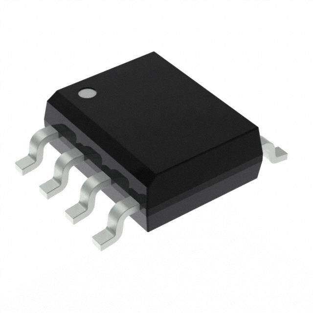
| 描述 | IC ECONOSCILLATOR SS 8-USOP可编程振荡器 Low-Frequency Spread Spctrm EconOscillatr |
| 产品分类 | |
| 品牌 | Maxim Integrated |
| 产品手册 | |
| 产品图片 |
|
| rohs | 符合RoHS无铅 / 符合限制有害物质指令(RoHS)规范要求 |
| 产品系列 | 振荡器,可编程振荡器,Maxim Integrated DS1090U-32+EconOscillator™ |
| 数据手册 | |
| 产品型号 | DS1090U-32+ |
| PLL | 无 |
| 产品 | Programmable |
| 产品培训模块 | http://www.digikey.cn/PTM/IndividualPTM.page?site=cn&lang=zhs&ptm=25703http://www.digikey.cn/PTM/IndividualPTM.page?site=cn&lang=zhs&ptm=25705 |
| 产品种类 | |
| 供应商器件封装 | 8-uMAX |
| 其它名称 | DS1090U32 |
| 其它有关文件 | |
| 分频器/倍频器 | 是/无 |
| 包装 | 管件 |
| 占空比-最大 | 55 % |
| 商标 | Maxim Integrated |
| 安装类型 | 表面贴装 |
| 安装风格 | SMD/SMT |
| 封装 | Tube |
| 封装/外壳 | 8-TSSOP,8-MSOP(0.118",3.00mm 宽) |
| 封装/箱体 | UMAX-8 |
| 尺寸 | 3 mm W x 3 mm L x 0.85 mm H |
| 工作温度 | -40°C ~ 85°C |
| 工厂包装数量 | 50 |
| 差分-输入:输出 | 无/无 |
| 应用说明 | 点击此处下载产品Datasheet点击此处下载产品Datasheet点击此处下载产品Datasheet点击此处下载产品Datasheet |
| 最大工作温度 | + 85 C |
| 最小工作温度 | - 40 C |
| 标准包装 | 50 |
| 比率-输入:输出 | 1:1 |
| 电压-电源 | 3 V ~ 5.5 V |
| 电源电压-最大 | 5.5 V |
| 电源电压-最小 | 3 V |
| 电路数 | 1 |
| 端接类型 | SMD/SMT |
| 类型 | 时钟发生器 |
| 系列 | DS1090U |
| 负载电容 | 30 pF |
| 输入 | 时钟 |
| 输出 | CMOS,TTL |
| 输出格式 | CMOS, TTL |
| 零件号别名 | 90-1090U+032 DS1090U |
| 频率 | 125 kHz to 250 kHz |
| 频率-最大值 | 250kHz |


- 商务部:美国ITC正式对集成电路等产品启动337调查
- 曝三星4nm工艺存在良率问题 高通将骁龙8 Gen1或转产台积电
- 太阳诱电将投资9.5亿元在常州建新厂生产MLCC 预计2023年完工
- 英特尔发布欧洲新工厂建设计划 深化IDM 2.0 战略
- 台积电先进制程称霸业界 有大客户加持明年业绩稳了
- 达到5530亿美元!SIA预计今年全球半导体销售额将创下新高
- 英特尔拟将自动驾驶子公司Mobileye上市 估值或超500亿美元
- 三星加码芯片和SET,合并消费电子和移动部门,撤换高东真等 CEO
- 三星电子宣布重大人事变动 还合并消费电子和移动部门
- 海关总署:前11个月进口集成电路产品价值2.52万亿元 增长14.8%


PDF Datasheet 数据手册内容提取
DS1090 Low-Frequency, Spread-Spectrum EconOscillator General Description Features The DS1090 is a low-cost, dithered oscillator intended ● Low-Cost, Spread-Spectrum EconOscillator™ to be used as an external clock for switched-mode ● Simple User Programming power supplies and other low-frequency applications. The ● O utput Frequency Programmable from 125kHz t o 8MHz dithering or sweeping function reduces peak-radiated emissions from the power supply at its fundamental ● Dither Percentage Programmable from 0% to 8% frequency, as well as harmonic frequencies. The device ● Dither Rate Programmable (fMOSC/512, 1024, 2048, consists of a resistor-programmed master oscillator, fac- or 4096) tory-programmed clock prescaler, and a pin-programmed ● 3.0V to 5.5V Single-Supply Operation dither circuit. These features allow the DS1090 to be used in applications where a spread-spectrum clock is desired ● CMOS/TTL-Compatible Output to reduce radiated emissions. A combination of factory-set ● Operating Temperature Range: -40°C to +85°C prescalers and external resistor allows for output frequencies ranging from 125kHz to 8MHz. Both dither frequency and Ordering Information dither percentage are set using control pins. OUTPUT PIN- PART FREQUENCY PRESCALER PACKAGE RANGE Applications DS1090U-1+ 4MHz to 8MHz 1 8 µSOP ● Switched-Mode Power Supplies DS1090U-2+ 2MHz to 4MHz 2 8 µSOP ● Servers ● Printers DS1090U-4+ 1MHz to 2MHz 4 8 µSOP ● Embedded Microcontrollers 500kHz to DS1090U-8+ 8 8 µSOP ● Industrial Controls 1MHz 250kHz to DS1090U-16+ 16 8 µSOP 500kHz 125kHz to DS1090U-32+ 32 8 µSOP Typical Operating Circuit 250kHz Add “T” for Tape & Reel orders. VIN VOUT Pin Configuration VCC DC-DC STEP-DOWN TOP VIEW CONVERTER VCC OUT JC0 OUT 1 8 JC1 DS1090 JC1 RSET 2 DS1090 7 JC0 RSET J0 45kΩ J1 VCC 3 6 J1 TO 91kΩ GND GND 4 5 J0 µSOP EconOscillator is a trademark of Maxim Integrated Products, Inc. 19-7500; Rev 3; 9/16
DS1090 Low-Frequency, Spread-Spectrum EconOscillator Absolute Maximum Ratings Voltage Range on VCC Relative to Ground .........-0.5V to +6.0V Operating Temperature Range ...........................-40°C to +85°C Voltage Range on Input Pins Storage Temperature Range ............................-55°C to +125°C Relative to Ground...............................-0.5V to (VCC + 0.5V), Soldering Temperature ......................................See IPC/JEDEC not to exceed 6.0V J-STD-020A Specification Stresses beyond those listed under “Absolute Maximum Ratings” may cause permanent damage to the device. These are stress ratings only, and functional operation of the device at these or any other conditions beyond those indicated in the operational sections of the specifications is not implied. Exposure to absolute maximum rating conditions for extended periods may affect device reliability. Recommended DC Operating Conditions (TA = -40°C to +85°C) PARAMETER SYMBOL CONDITIONS MIN TYP MAX UNITS Supply Voltage VCC (Note 1) 3.0 5.5 V Input Logic 1 (J0, J1, JC0, JC1) VIH 0V.C7 Cx VC0.C3 + V +0.3 x Input Logic 0 (J0, J1, JC0, JC1) VIL -0.3 VCC V DC Electrical Characteristics (VCC = +3.0V to +5.5V, TA = -40°C to +85°C, unless otherwise noted.) PARAMETER SYMBOL CONDITIONS MIN TYP MAX UNITS CL = 15pF, VCC = 3.3V, RSET = 40kΩ 1.4 Supply Current ICC mA CL = 15pF, VCC = 5.5V, RSET = 40kΩ 1.7 3 IOH = -4mA High-Level Output Voltage (OUT) VOH 2.4 V VCC = min Low-Level Output Voltage (OUT) VOL IOL = 4mA 0.4 V High-Level Input Current (J0, J1, JC0, JC1) IIH VIH = VCC +1.0 µA Low-Level Input Current (J0, J1, JC0, JC1) IIL VIL = 0V -1.0 µA Resistor Current IRES VCC = max 150 µA www.maximintegrated.com Maxim Integrated │ 2
DS1090 Low-Frequency, Spread-Spectrum EconOscillator AC Electrical Characteristics (VCC = +3.0V to +5.5V, TA = -40°C to +85°C, unless otherwise noted.) PARAMETER SYMBOL CONDITIONS MIN TYP MAX UNITS Internal Master Oscillator Frequency fMOSC 4.0 8.0 MHz Output Frequency Tolerance ∆fOUT VTAC C= =+ 235.3°CV, -3.0 +3.0 % TA = +25°C, RSET = 60kΩ, -0.5 +0.5 VCC = 3.0V to 3.6V (Notes 2, 3) Voltage Frequency Variation ∆fOUT % TA = +25°C, RSET = 60kΩ, -1.25 +1.25 VCC = 4.5V to 5.5V (Notes 2, 3) Temperature Frequency Variation ∆fOUT V(NCoCte =s 32.,3 3V, 4) -2.0 +2.0 % J0 = GND, J1 = GND 0 Peak-to-Peak Dither (3σ) J0 = VCC, J1 = GND 2 % (Note 5) J0 = GND, J1 = VCC 4 J0 = VCC, J1 = VCC 8 Power-Up Time tPOR + (Note 6) 0.1 0.5 ms tSTAB Load Capacitance CL (Note 7) 30 pF 4MHz to 8MHz, TA = +25°C (Note 3) 45 55 Output Duty Cycle % <4MHz (Note 4) 50 Output Rise/Fall Time tR, tF CL = 15pF 20 ns Note 1: All voltages referenced to ground. Note 2: This is the change observed in output frequency due to changes in temperature or voltage. Note 3: See the Typical Operating Characteristics section. Note 4: Parameter is guaranteed by design and is not production tested. Note 5: This is a percentage of the output period. Parameter is characterized but not production tested. This can be varied from 0% to 8%. Note 6: This indicates the time between power-up and the outputs becoming active. An on-chip delay is intentionally introduced to allow the oscillator to stabilize. tSTAB is equivalent to ~500 clock cycles and is dependent upon the programmed output frequency. Note 7: Output voltage swings can be impaired at high frequencies combined with high output loading. www.maximintegrated.com Maxim Integrated │ 3
DS1090 Low-Frequency, Spread-Spectrum EconOscillator Typical Operating Characteristics (VCC = +3.3V, TA = +25°C, unless otherwise noted.) SUPPLY CURRENT SUPPLY CURRENT SUPPLY CURRENT vs. SUPPLY VOLTAGE vs. TEMPERATURE vs. OUTPUT LOADING 1.70 NO LOAD, TA = +25°C DS1090 toc01 11..3500 NO LOAD, VCC = 3.3V DS1090 toc02 4 TA = +25°C, RSET = 40kΩ DS1090 toc03 mA)1.45 mA) 40kΩ mA) 3 5V RENT ( 40kΩ RENT (1.10 RENT ( 4V UR1.20 UR 60kΩ UR 2 3V C 60kΩ C C UPPLY UPPLY 0.90 UPPLY S0.95 S S 1 0.70 80kΩ 80kΩ 0.70 0.50 0 3.0 3.5 4.0 4.5 5.0 5.5 -40 -15 10 35 60 85 5 10 15 20 25 30 35 40 SUPPLY VOLTAGE (V) TEMPERATURE (°C) LOAD CAPACITANCE (pF) OUTPUT VOLTAGE HIGH OUTPUT VOLTAGE LOW OUTPUT FREQUENCY vs. OUTPUT CURRENT vs. OUTPUT CURRENT vs. SUPPLY VOLTAGE 3.1 VCC = 3.0V DS1090 toc04 0.4 VCC = 3.0V DS1090 toc05 190 TA = +25°C DS1090 toc06 E (V) 3.0 E (V) 0.3 Hz) 8 40kΩ G G M TA TA Y ( T VOL 2.9 T VOL 0.2 UENC 7 60kΩ U U Q UTP UTP FRE 6 80kΩ O O 2.8 0.1 5 2.7 0 4 -5 -4 -3 -2 -1 0 0 1 2 3 4 5 3.0 3.5 4.0 4.5 5.0 5.5 OUTPUT CURRENT (mA) OUTPUT CURRENT (mA) SUPPLY VOLTAGE (V) www.maximintegrated.com Maxim Integrated │ 4
DS1090 Low-Frequency, Spread-Spectrum EconOscillator Typical Operating Characteristics (continued) (VCC = +3.3V, TA = +25°C, unless otherwise noted.) OUTPUT FREQUENCY DUTY CYCLE RESISTOR CURRENT vs. TEMPERATURE vs. TEMPERATURE vs. RESISTOR VALUE 109 VCC = 3.3V DS1090 toc07 5512 RSET = 40kΩ DS1090 toc08 mA) 1168 VCC = 3.3V, TA = +25°C DS1090 toc09 EQUENCY (MHz) 78 80kΩ 60kΩ 40kΩ UTY CYCLE (%) 50 VCC = 3.3V TOR CURRENT ( 1124 FR 6 D 49 VCC = 5V RESIS 10 5 DS1090U-1 4 48 8 -40 -15 10 35 60 85 -40 -15 10 35 60 85 40 50 60 70 80 TEMPERATURE (°C) TEMPERATURE (°C) RSET (kΩ) FREQUENCY ERROR FREQUENCY ERROR vs. SUPPLY VOLTAGE (FROM 3.3V) vs. TEMPERATURE (FROM +25°C) POWER SPECTRUM vs. SPREAD 5.0 TA = +25°C DS1090 toc10 2.0 VCC = 3.3V 60kΩ DS1090 toc11 -100 OFF JVTCAC 0C= ==+ 2J3C5.3°1VC =,, 1DS1090 toc12 %) 2.5 %) 1.0 -20 R ( R ( 2% CY ERRO 0 80kΩ CY ERRO 0 ER (dBm) --4300 4% N N W 8% EQUE EQUE 80kΩ PO -50 R R F -2.5 40kΩ F -1.0 -60 60kΩ 40kΩ -70 -5.0 -2.0 -80 3.0 3.5 4.0 4.5 5.0 5.5 -40 -15 10 35 60 85 4.80 5.35 5.90 SUPPLY VOLTAGE (V) TEMPERATURE (°C) FREQUENCY (MHz) www.maximintegrated.com Maxim Integrated │ 5
DS1090 Low-Frequency, Spread-Spectrum EconOscillator Pin Description PIN NAME FUNCTION 1 OUT Oscillator Output 2 RSET Frequency Control Resistor Input 3 VCC Positive-Supply Terminal 4 GND Ground 5 J0 Dither Amplitude (Percentage) Inputs 6 J1 (see Table 2) 7 JC0 Dither Rate Divisor Inputs (see Table 1) 8 JC1 Block Diagram DS1090 RSET VOLTAGE- BIAS CIRCUIT MASTER + OSCILLATOR fMOSC PROFAGCRTAOMRMYED fOSC fOUT ∑ (VCO) PRESCALER BUFFER OUT + ( 1, 2, 4, 8, 16, OR 32) 4MHz–8MHz VCC VCC DITHER GENERATOR + DITHER TRIANGLE GND - AMPLITUDE GENERATOR DITHER RATE (0, 2, 4, OR 8%) fMOD ( 128) ( 4, 8, 16, OR 32) J0 J1 JC0 JC1 www.maximintegrated.com Maxim Integrated │ 6
DS1090 Low-Frequency, Spread-Spectrum EconOscillator MASTER OSCILLATOR FREQUENCY vs. IF DITHER AMOUNT = 0% EXTERNAL RESISTOR SELECTION 89 DS1090 fig01 ((+- 11P,, 22ro,, goorrra 44m%%m ooeffd ff MMfMOOOSSSCCC)) DA(2MI,T 4OH,U EORNRT 8%) 1 7 MOSC fMOD Hz) f M (C 6 OS TIME M f 5 Figure 2. Center Frequency Dither Diagram 4 Factory-Programmed Prescaler 3 40 50 60 70 80 90 The prescaler divides the frequency of the master oscillator RSET RESISTANCE (kΩ) by 1, 2, 4, 8, 16, or 32 to generate the square-wave output clock (fOSC). This divisor is factory-set and is an ordering Figure 1. Master Oscillator Frequency option. Detailed Description Dither Generator The DS1090 is a center-dithered, spread-spectrum silicon Spread-spectrum functionality is achieved by a user- oscillator for use as an external clock in reduced-EMI configurable divider (determines dither rate), a triangle applications. With a combination of factory-programmed generator, and a user-configurable dither amplitude circuit prescalers and a user-selected external resistor, output (see Block Diagram). frequencies from 125kHz to 8MHz can be achieved. The The input to the triangle-wave generator is derived output center frequency can be dithered by selecting the from the internal master oscillator and is fed through a desired dither rate and amplitude with discrete inputs J0, user-configurable divider. The settings of control pins JC0 J1, JC0, and JC1. and JC1 determine this dither rate divisor setting (see The DS1090 contains four basic circuit blocks: master Table 1), dividing the master clock by 4, 8, 16, or 32. The oscillator, factory-programmed prescaler, dither generator, clock signal is further divided by 128 in the triangle-wave and the voltage-bias circuit that provides the feedback generator, which results in a triangle-wave signal of either path to the master oscillator for frequency control and 1/512th, 1/1024th, 1/2048th, or 1/4096th of the master dithering functions. oscillator (fMOD), depending upon the user’s divisor set- ting. Master Oscillator The dithering frequency can be also expressed as the The master oscillator is programmable in the application result of by the use of an external resistor (RSET) tied to ground (GND). Resistor values of 45kΩ to 91kΩ vary the square-wave output frequency of the voltage-controlled fMOD=DivfiMsoOrS×C128 master oscillator (fMOSC) from 8MHz down to 4MHz (see Figure 1). where Divisor is 4, 8, 16, or 32. The master oscillator (Hz) frequency can be stated as Table 1. Dither Rate Divisor Settings 3.6461 E+11 fMOSC≅ Resistor DITHERING PERCENTAGE DIVISOR JC1 JC0 (fMOSC/n) SETTING 0 0 fMOSC /512 4 0 1 fMOSC /1024 8 1 0 fMOSC /2048 16 1 1 fMOSC /4096 32 www.maximintegrated.com Maxim Integrated │ 7
DS1090 Low-Frequency, Spread-Spectrum EconOscillator Table 2. Dither Percentage Setting RSET Resistor Selection The value of the resistor used to select the desired J1 J0 DITHER PERCENT (%) frequency is calculated using the formula in the Master 0 0 0 Oscillator section (see also Figure 1). It is recommended 0 1 2 to use, at minimum, a 1%-tolerance, 1/16th-watt component 1 0 4 with a temperature coefficient that satisfies the overall stability requirements desired of the end-equipment. 1 1 8 Place the external RSET resistor as close as possible to Dither Percentage Settings minimize lead inductance. Dither amplitude (measured in percent ± from the master Power-Supply Decoupling oscillator center frequency) is set using input pins J0 and To achieve best results, it is highly recommended that a J1. This circuit uses a sense current from the master decoupling capacitor is used on the IC power-supply pins. oscillator bias circuit to adjust the amplitude of the tri- Typical values of decoupling capacitors are 0.01µF and angle-wave signal to a voltage level that modulates the 0.1µF. Use a high-quality, ceramic, surface-mount capaci- master oscillator to a percentage of its resistor-set center tor, and mount it as close as possible to the VCC and GND frequency. This percentage is set in the end application to pins of the IC to minimize lead inductance. be 0%, 2%, 4%, or 8% (see Table 2). Application Information Chip Information SUBSTRATE CONNECTED TO GROUND Pin Connection The DS1090 is intended to provide a fixed-frequency, dithered clock to be used as a clock driver for DC-DC converters and other applications requiring a low- Package Information frequency EMI-reduced clock oscillator. All control pins For the latest package outline information and land patterns must be biased per Tables 1 and 2 for proper operation (footprints), go to www.maximintegrated.com/packages. Note for the individual application’s requirements. RSET must that a “+”, “#”, or “-” in the package code indicates RoHS status be tied to ground (GND) by a customer-supplied resistor. only. Package drawings may show a different suffix character, but the drawing pertains to the package regardless of RoHS status. www.maximintegrated.com Maxim Integrated │ 8
DS1090 Low-Frequency, Spread-Spectrum EconOscillator Revision History REVISION REVISION PAGES DESCRIPTION NUMBER DATE CHANGED 1 2/07 — — 2 2/15 Remove automotive reference from data sheet 1 3 9/16 Corrected typo in Benefits and Features section 1 For pricing, delivery, and ordering information, please contact Maxim Direct at 1-888-629-4642, or visit Maxim Integrated’s website at www.maximintegrated.com. Maxim Integrated cannot assume responsibility for use of any circuitry other than circuitry entirely embodied in a Maxim Integrated product. No circuit patent licenses are implied. Maxim Integrated reserves the right to change the circuitry and specifications without notice at any time. The parametric values (min and max limits) shown in the Electrical Characteristics table are guaranteed. Other parametric values quoted in this data sheet are provided for guidance. Maxim Integrated and the Maxim Integrated logo are trademarks of Maxim Integrated Products, Inc. © 2016 Maxim Integrated Products, Inc. │ 9
Mouser Electronics Authorized Distributor Click to View Pricing, Inventory, Delivery & Lifecycle Information: M axim Integrated: DS1090U-1+ DS1090U-1+T DS1090U-16+ DS1090U-16+T DS1090U-2+ DS1090U-2+T DS1090U-32+ DS1090U-32+T DS1090U-4+ DS1090U-4+T DS1090U-8+T DS1090U-2/V+ DS1090U-8+ DS1090U-2/V+T DS1090U-8/V+ DS1090U-8/V+T