ICGOO在线商城 > 集成电路(IC) > 时钟/计时 - 时钟发生器,PLL,频率合成器 > ISPPAC-CLK5620AV-01TN100C
 Datasheet下载
- 型号: ISPPAC-CLK5620AV-01TN100C
- 制造商: Lattice
- 库位|库存: xxxx|xxxx
- 要求:
| 数量阶梯 | 香港交货 | 国内含税 |
| +xxxx | $xxxx | ¥xxxx |
查看当月历史价格
查看今年历史价格
ISPPAC-CLK5620AV-01TN100C产品简介:
ICGOO电子元器件商城为您提供ISPPAC-CLK5620AV-01TN100C由Lattice设计生产,在icgoo商城现货销售,并且可以通过原厂、代理商等渠道进行代购。 ISPPAC-CLK5620AV-01TN100C价格参考。LatticeISPPAC-CLK5620AV-01TN100C封装/规格:时钟/计时 - 时钟发生器,PLL,频率合成器, 。您可以下载ISPPAC-CLK5620AV-01TN100C参考资料、Datasheet数据手册功能说明书,资料中有ISPPAC-CLK5620AV-01TN100C 详细功能的应用电路图电压和使用方法及教程。
Lattice Semiconductor Corporation的ISPPAC-CLK5620AV-01TN100C是一款可编程时钟发生器、锁相环(PLL)和频率合成器芯片,广泛应用于需要高精度、多路时钟信号生成与管理的场景。

该器件主要应用于通信设备、网络设备、工业控制系统、测试与测量仪器以及消费类电子产品中。其主要功能是生成多种频率和相位的时钟信号,满足系统中不同模块对时钟源的需求。

该芯片支持灵活的频率合成和分频设置,适用于需要高性能时钟管理的场合,如FPGA、ASIC、高速ADC/DAC、处理器系统等的时钟源配置。同时,其可编程特性使其能够适应多种应用需求,提升系统设计的灵活性和可维护性。

此外,ISPPAC-CLK5620AV-01TN100C具备低抖动、高稳定性等特点,适合对信号完整性要求较高的高速数字系统和射频应用。
| 参数 | 数值 |
| 产品目录 | 集成电路 (IC)半导体 |
| 描述 | IC CLOCK PROGRAM BUFFER 100TQFP时钟驱动器及分配 ISP 0 Dlay Clck Gen w/Unv Fan-Out Buf I |
| 产品分类 | |
| 品牌 | Lattice Semiconductor Corporation |
| 产品手册 | |
| 产品图片 |
|
| rohs | 符合RoHS无铅 / 符合限制有害物质指令(RoHS)规范要求 |
| 产品系列 | 时钟和计时器IC,时钟驱动器及分配,Lattice ispPAC-CLK5620AV-01TN100CispClock™ |
| mouser_ship_limit | 此产品可能需要其他文件才能从美国出口。 |
| 数据手册 | 点击此处下载产品Datasheethttp://www.latticesemi.com/~/media/Documents/DataSheets/ispClock/ispClock5600FamilyDataSheet.PDF?document_id=9110 |
| 产品型号 | ISPPAC-CLK5620AV-01TN100C |
| PLL | 带旁路 |
| 乘法/除法因子 | 2:20 |
| 产品种类 | 时钟驱动器及分配 |
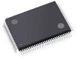
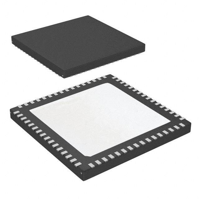
| 供应商器件封装 | 100-TQFP(14x14) |
| 其它名称 | 220-1629 |
| 分频器/倍频器 | 是/无 |
| 包装 | 托盘 |
| 商标 | Lattice |
| 安装类型 | 表面贴装 |
| 安装风格 | SMD/SMT |
| 封装 | Tray |
| 封装/外壳 | 100-LQFP |
| 封装/箱体 | TQFP-100 |
| 工作温度 | 0°C ~ 70°C |
| 工厂包装数量 | 90 |
| 差分-输入:输出 | 是/是 |
| 最大功率耗散 | 1.75 W |
| 最大工作温度 | + 70 C |
| 最大输出频率 | 400 MHz |
| 最小工作温度 | 0 C |
| 标准包装 | 90 |
| 比率-输入:输出 | 2:20 |
| 电压-电源 | 3 V ~ 3.6 V |
| 电源电压-最大 | 3.6 V |
| 电源电压-最小 | 3 V |
| 电源电流 | 130 mA |
| 电路数 | 1 |
| 类型 | * |
| 系列 | CLK5620AV-01TN |
| 输入 | HSTL,LVCMOS,LVDS,LVPECL,LVTTL,SSTL |
| 输入类型 | HSTL, LVCMOS, LVDS, LVPECL, LVTTL, SSTL |
| 输出 | EHSTL,HSTL,LVCMOS,LVDS,LVPECL,LVTTL,SSTL |
| 输出类型 | EHSTL, HSTL, LVCMOS, LVDS, LVPECL, LVTTL, SSTL |
| 频率-最大值 | 400MHz |

.jpg)


- 商务部:美国ITC正式对集成电路等产品启动337调查
- 曝三星4nm工艺存在良率问题 高通将骁龙8 Gen1或转产台积电
- 太阳诱电将投资9.5亿元在常州建新厂生产MLCC 预计2023年完工
- 英特尔发布欧洲新工厂建设计划 深化IDM 2.0 战略
- 台积电先进制程称霸业界 有大客户加持明年业绩稳了
- 达到5530亿美元!SIA预计今年全球半导体销售额将创下新高
- 英特尔拟将自动驾驶子公司Mobileye上市 估值或超500亿美元
- 三星加码芯片和SET,合并消费电子和移动部门,撤换高东真等 CEO
- 三星电子宣布重大人事变动 还合并消费电子和移动部门
- 海关总署:前11个月进口集成电路产品价值2.52万亿元 增长14.8%


PDF Datasheet 数据手册内容提取
ispClock™ 5600A Family In-System Programmable, Enhanced Zero-Delay Clock Generator with Universal Fan-Out Buffer June 2008 Data Sheet DS1019 Features ■ Up to Five Clock Frequency Domains ■ 8MHz to 400MHz Input/Output Operation ■ Flexible Clock Reference and External Feedback Inputs ■ Low Output to Output Skew (<50ps) • Programmable input standards ■ Low Jitter Peak-to-Peak - LVTTL, LVCMOS, SSTL, HSTL, LVDS, ■ Up to 20 Programmable Fan-out Buffers LVPECL, Differential HSTL, SSTL • Programmable output standards and individual • Clock A/B selection multiplexer enable controls • Feedback A/B selection multiplexer - LVTTL, LVCMOS, HSTL, eHSTL, SSTL, • Programmable termination LVDS, LVPECL, Differential HSTL, SSTL ■ All Inputs and Outputs are Hot Socket • Programmable output impedance Compliant - 40 to 70Ω in 5Ω increments ■ Four User-programmable Profiles Stored in • Programmable slew rate E2CMOS® Memory • Up to 10 banks with individual VCCO and GND • Supports both test and multiple operating - 1.5V, 1.8V, 2.5V, 3.3V configurations ■ Fully Integrated High-Performance PLL ■ Full JTAG Boundary Scan Test In-System • Programmable lock detect Programming Support • Multiply and divide ratio controlled by ■ Exceptional Power Supply Noise Immunity - Input divider (1 to 40) ■ Commercial (0 to 70°C) and Industrial - Feedback divider (1 to 40) (-40 to 85°C) Temperature Ranges - Five output dividers (2 to 80) ■ 100-pin and 48-pin TQFP Packages • Programmable on-chip loop filter • Compatible with spread spectrum clocks ■ Applications ■ Precision Programmable Phase Adjustment • Circuit board common clock generation and (Skew) Per Output distribution • 16 settings; minimum step size 156ps • PLL-based frequency generation - Locked to VCO frequency • High fan-out clock buffer • Up to +/- 12ns skew range • Zero-delay clock buffer • Coarse and fine adjustment modes Product Family Block Diagram LOCK DETECT OUTPUT DIVIDERS SKEW OUTPUT V0 CONTROL DRIVERS E BYPASS C MUX REFERENINPUTS * M FREPQHAUSEEN/CY FILTER VCO VV12 DETECTOR V3 TS N PLL CORE V4 ROOUUTTPIUNTG OUTPU MATRIX K C O InteFrneaeld/Ebxatcekrnal JTAG CL EDBACKNPUTS * Select INMET2EECMR&MOFOARSCYE M0aMnualgt1iepmlee Pnr2to Lfoilegi3c EI F INTERNAL FEEDBACK PATH * Input Available only on ispClock5620A © 2008 Lattice Semiconductor Corp. All Lattice trademarks, registered trademarks, patents, and disclaimers are as listed at www.latticesemi.com/legal. All other brand or product names are trademarks or registered trademarks of their respective holders. The specifications and information herein are subject to change without notice. www.latticesemi.com 1-1 DS1019_01.4
Lattice Semiconductor ispClock5600A Family Data Sheet General Description and Overview The ispClock5610A and ispClock5620A are in-system-programmable high-fanout enhanced zero delay clock gen- erators designed for use in high performance communications and computing applications. The ispClock5610A provides up to 10 single-ended or five differential clock outputs, while the ispClock5620A provides up to 20 single- ended or 10 differential clock outputs. Each pair of outputs may be independently configured to support separate I/O standards (LVDS, LVPECL, LVTTL, LVCMOS, SSTL, HSTL) and output frequency. In addition, each output provides independent programmable control of termination, slew-rate, and timing skew. All configuration informa- tion is stored on-chip in non-volatile E2CMOS memory. The ispClock5600A’s PLL and divider systems supports the synthesis of multiple clock frequencies derived from the reference input through the provision of programmable input and feedback dividers. A set of five post-PLL V- dividers provides additional flexibility by supporting the generation of five separate output frequencies. Loop feed- back may be taken internally from the output of any of the five V-dividers, or externally through FBKA+/- or FBKB+/- pins. The core functions of all members of the ispClock5600A family are identical, the differences between devices being restricted to the number of inputs and outputs, as shown in the following table. Figures 1 and 2 show functional block diagrams of the ispClock5610A and ispClock5620A. Table 1-1. ispClock5600A Family Members Device Ref. Input Pairs Feedback Input Pairs Clock Outputs ispClock5610A 1 1 10 ispClock5620A 2 2 20 Figure 1-1. ispClock5610A Functional Block Diagram PS0 PS1 LOCK RESET PLL_BYPASS SGATE GOE OEX OEY Profile Select Control OUTPUT ENABLE CONTROLS 0 1 2 3 LOCK DETECT OUTPUT ROUTING SKEW OUTPUT MATRIX CONTROL DRIVERS OUTPUT BANK_0 DIVIDERS V0 BANK_0 (2-80) BANK_1 INPUT V1 BANK_1 DIVIDER (2-80) BANK_2 REFA+ M RERFEVFTAT- (1-40) DPEHTAESCET FLILOTOEPR VCO 10 (2V-820) BBAANNKK__32 V3 BANK_3 (2-80) BANK_4 N FEEDBACK V4 BANK_4 (1-40) DIVIDER (2-80) E2 Configuration SKFEEWED ABDAJCUKST FBKA+ FBKA - FBKVTT JTAG INTERFACE TDI TMS TCK TDO 1-2
Lattice Semiconductor ispClock5600A Family Data Sheet Figure 1-2. ispClock5620A Functional Block Diagram PS0 PS1 LOCK RESET PLL_BYPASS SGATE GOE OEX OEY OUTPUT ROUTING SKEW OUTPUT Profile Select MATRIX CONTROL DRIVERS Control OUTPUT ENABLE CONTROLS BANK_0A 0 1 2 3 BANK_0B BANK_1A DLEOTCECKT BANK_1B BANK_2A BANK_2B OUTPUT BANK_3A DIVIDERS V0 BANK_3B REFSEL (2-80) BANK_4A REFA+ INPUT V1 BANK_4B REFA- DIVIDER (2-80) 0 M RREEFFVBTT+ 1 (1-40) DPEHTAESCET FLILOTOEPR VCO 10 (2V-820) SKEW OUTPUT REFB- CONTROL DRIVERS V3 (2-80) BANK_5A BANK_5B N FEEDBACK V4 (1-40) DIVIDER (2-80) BANK_6A FBKSEL BANK_6B FBKA+ E2 Configuration BANK_7A FBKA- BANK_7B 0 FBKVTT 1 BANK_8A FBKB+ FBKB- BANK_8B BANK_9A JTAG INTERFACE FEEDBACK SKEW ADJUST BANK_9B TDI TMS TCK TDO 1-3
Lattice Semiconductor ispClock5600A Family Data Sheet Absolute Maximum Ratings ispClock5600A Core Supply Voltage V . . . . . . . . . . . . . . . . . . . -0.5 to 5.5V CCD PLL Supply Voltage V . . . . . . . . . . . . . . . . . . . . -0.5 to 5.5V CCA JTAG Supply Voltage V . . . . . . . . . . . . . . . . . . . -0.5 to 5.5V CCJ Output Driver Supply Voltage V . . . . . . . . . . . . -0.5 to 4.5V CCO Input Voltage . . . . . . . . . . . . . . . . . . . . . . . . . . . . . -0.5 to 4.5V Output Voltage1 . . . . . . . . . . . . . . . . . . . . . . . . . . . -0.5 to 4.5V Storage Temperature . . . . . . . . . . . . . . . . . . . . . . . -65 to 150°C Junction Temperature with power supplied . . . . . . -40 to 130°C 1. When applied to an output when in high-Z condition Recommended Operating Conditions ispClock5600A Symbol Parameter Conditions Min. Max. Units V Core Supply Voltage 3.0 3.6 V CCD V JTAG I/O Supply Voltage 2.25 3.6 V CCJ V Analog Supply Voltage 3.0 3.6 V CCA V V Turn-on Ramp Rate All supply pins — 0.33 V/µs CCXSLEW CC Commercial 0 130 T Operating Junction Temperature °C JOP Industrial -40 130 Commercial 0 701 T Ambient Operating Temperature °C A Industrial -40 851 1. Device power dissipation may also limit maximum ambient operating temperature. Recommended Operating Conditions – V vs. Logic Standard CCO V (V) V (V) V (V) CCO REF TT Logic Standard Min. Typ. Max. Min. Typ. Max. Min. Typ. Max. LVTTL 3.0 3.3 3.6 — — — — — — LVCMOS 1.8V 1.71 1.8 1.89 — — — — — — LVCMOS 2.5V 2.375 2.5 2.625 — — — — — — LVCMOS 3.3V 3.0 3.3 3.6 — — — — — — SSTL1.8 1.71 1.8 1.89 0.84 0.90 0.95 — 0.5 x V — CCO SSTL2 Class 1 2.375 2.5 2.625 1.15 1.25 1.35 V - 0.04 V V + 0.04 REF REF REF SSTL3 Class 1 3.0 3.3 3.6 1.30 1.50 1.70 V - 0.05 V V + 0.05 REF REF REF HSTL Class 1 1.425 1.5 1.575 0.68 0.75 0.90 — 0.5 x V — CCO eHSTL Class 1 1.71 1.8 1.89 0.84 0.90 0.95 — 0.5 x V — CCO LVPECL (Differential) 3.0V 3.3V 3.6V — — — — — — V = 2.5V 2.375 2.5V 2.625 — — — — — — CCO LVDS V = 3.3V 3.0 3.3 3.6 — — — — — — CCO Note: ‘—’ denotes V or V not applicable to this logic standard REF TT 1-4
Lattice Semiconductor ispClock5600A Family Data Sheet E2CMOS Memory Write/Erase Characteristics Parameter Conditions Min. Typ. Max. Units Erase/Reprogram Cycles 1000 — — Performance Characteristics – Power Supply Symbol Parameter Conditions Typ. Max. Units ispClock5610A f = 800MHz 110 125 mA I Core Supply Current3 VCO CCD ispClock5620A f = 800MHz 130 150 mA VCO I Analog Supply Current3 f = 800MHz 5.5 7 mA CCA VCO V = 1.8V1, LVCMOS, f = 266MHz 16 18 mA CCO OUT Output Driver Supply Current VCCO = 2.5V1, LVCMOS, fOUT = 266MHz 21 27 mA I CCO (per Bank) V = 3.3V1, LVCMOS, f = 266MHz 27 38 mA CCO OUT V = 3.3V2, LVDS, f = 400MHz 8 10 mA CCO OUT V = 1.8V 300 µA CCJ I JTAG I/O Supply Current (static) V = 2.5V 400 µA CCJ CCJ V = 3.3V 400 µA CCJ 1. Supply current consumed by each bank, both outputs active, 5pF load. 2. Supply current consumed by each bank, 100Ω, 5pf differential load. 3. All unused REFCLK and feedbacks connected to ground. DC Electrical Characteristics – Single-ended Logic V (V) V (V) IL IH Logic Standard Min. Max. Min. Max. V Max. (V) V Min. (V) I (mA) I (mA) OL OH OL OH LVTTL/LVCMOS 3.3V -0.3 0.8 2 3.6 0.4 V - 0.4 122, 3 -122, 3 CCO LVCMOS 1.8V -0.3 0.68 1.07 3.6 0.4 V - 0.4 122, 3 -122, 3 CCO LVCMOS 2.5V -0.3 0.7 1.7 3.6 0.4 V - 0.4 122, 3 -122, 3 CCO SSTL2 Class 1 -0.3 V - 0.18 V + 0.18 3.6 0.542 V - 0.811 7.6 -7.6 REF REF CCO SSTL3 Class 1 -0.3 V - 0.2 V + 0.2 3.6 0.92 V - 1.31 8 -8 REF REF CCO HSTL Class 1 -0.3 V - 0.1 V + 0.1 3.6 0.43 V - 0.42 8 -8 REF REF CCO eHSTL Class 1 -0.3 V - 0.1 V + 0.1 3.6 0.43 V - 0.42 8 -8 REF REF CCO 1. Specified for 40Ω internal series output termination. 2. Specified for ≈20Ω internal series output termination, fast slew rate setting. 3. For slower slew rate setting I , I = 8mA. OH OL 1-5
Lattice Semiconductor ispClock5600A Family Data Sheet DC Electrical Characteristics – LVDS Symbol Parameter Conditions Min. Typ. Max. Units VTHD ≤ 100mV VTHD/2 — 2.0 V V Common Mode Input Voltage ICM VTHD ≤ 150mV VTHD/2 2.325 V V Differential Input Threshold ±100 — — mV THD V Input Voltage 0 — 2.4 V IN VOH Output High Voltage RT = 100Ω — 1.375 1.60 V VOL Output Low Voltage RT = 100Ω 0.9 1.03 — V VOD Output Voltage Differential RT = 100Ω 250 400 480 mV ΔVOD Change in VOD Between H and L — — 50 mV V Output Voltage Offset Common Mode Output Voltage 1.10 1.20 1.375 V OS ΔVOS Change in VOS Between H and L — — 50 mV I Output Short Circuit Current V = 0V, Outputs Shorted to GND — — 24 mA SA OD I Output Short Circuit Current V = 0V, Outputs Shorted to Each Other — — 12 mA SAB OD DC Electrical Characteristics – Differential LVPECL Symbol Parameter Test Conditions Min. Typ. Max. Units V = 3.0 to 3.6V V - 1.17 — V - 0.88 CCD CCD CCD V Input Voltage High V IH V = 3.3V 2.14 — 2.42 CCD V = 3.0 to 3.6V V - 1.81 — V - 1.48 CCD CCD CCD V Input Voltage Low V IL V = 3.3V 1.49 — 1.83 CCD V = 3.0 to 3.6V V - 1.07 — V - 0.88 V Output High Voltage1 CCO CCO CCO V OH V = 3.3V 2.23 — 2.42 CCO V = 3.0 to 3.6V V - 1.81 — V - 1.62 V Output Low Voltage1 CCO CCO CCO V OL V = 3.3V 1.49 — 1.68 CCO 1. 100Ω differential termination. Electrical Characteristics – Differential SSTL18 Symbol Parameter Conditions Min. Typ. Max. Units V Output Supply Voltage 1.71 1.8 1.89 V CCO V Low-Logic Level Input Voltage 0.61 V IL V Hi Logic Level Input Voltage 1.17 V IH V AC Differential Output Voltage 0.64 V SWING Input Pair Differential Crosspoint V V -175mV V +175mV V IX Voltage REF REF Load Conditions TCKD Clock Duty Cycle 45 55 % (Figure 1-6) 1-6
Lattice Semiconductor ispClock5600A Family Data Sheet Electrical Characteristics – Differential SSTL2 Symbol Parameter Conditions Min. Typ. Max. Units V Output Supply Voltage 2.375 2.5 2.625 V CCO V DC Differential Input Voltage Swing -0.03 3.225 V SWING(DC) V AC Input Differential Voltage 0.62 3.225 V SWING(AC) Input Pair Differential Crosspoint V V - 200 mV V + 200 mV V IX Voltage REF REF Load Conditions TCKD Clock Duty Cycle 45 55 % (Figure 1-6) Electrical Characteristics – Differential HSTL Symbol Parameter Conditions Min Typ Max Units V Output Supply Voltage 1.425 1.5 1.575 V CCO V DC Differential Input Voltage Swing -0.03 V V SWING(DC) CCD V AC Input Differential Voltage 0.4 V V SWING(AC) CCD Input Pair Differential Crosspoint V 0.68 0.9 V IX Voltage Load Conditions TCKD Clock Duty Cycle 45 55 % (Figure 1-6) Electrical Characteristics – Differential eHSTL Symbol Parameter Conditions Min Typ Max Units V Output Supply Voltage 1.7 1.8 1.9 V CCO V DC Differential Input Voltage Swing -0.03 V V SWING(DC) CCD V AC Input Differential Voltage 0.4 V V SWING(AC) CCD Input Pair Differential Crosspoint V 0.68 0.9 V IX Voltage Load Conditions TCKD Clock Duty Cycle 45 55 % (Figure 1-6) DC Electrical Characteristics – Input/Output Loading Symbol Parameter Conditions Min. Typ. Max. Units I Input Leakage Note 1 — — ±10 µA LK I Input Pull-up Current Note 2 — 80 120 µA PU I Input Pull-down Current Note 3 — 120 150 µA PD I Tristate Leakage Output Note 4 — — ±10 µA OLK Notes 2, 3, 5 — 8 10 pF C Input Capacitance IN Note 6 — 13.5 15 pF 1. Applies to clock reference inputs when termination ‘open’. 2. Applies to TDI, TMS inputs. 3. Applies to REFSEL, PS0, PS1, GOE, SGATE and PLL_BYPASS, FBKSEL, OEX, OEY. 4. Applies to all logic types when in tristated mode. 5. Applies to OEX, OEY, TCK, RESET inputs. 6. Applies to REFA+, REFA-, REFB+, REFB-, FBKA+, FBKA-, FBKB+, FBKB-. 1-7
Lattice Semiconductor ispClock5600A Family Data Sheet Switching Characteristics – Timing Adders for I/O Modes Adder Type Description Min. Typ. Max. Units t Input Adders2 IOI LVTTL_in Using LVTTL Standard 0 0 0 ps LVCMOS18_in Using LVCMOS 1.8V Standard -99 80 315 ps LVCMOS25_in Using LVCMOS 2.5V Standard 0 0 0 ps LVCMOS33_in Using LVCMOS 3.3V Standard 0 0 0 ps SSTL18_in Using SSTL18 Standard 10 360 642 ps SSTL2_in Using SSTL2 Standard 64 420 679 ps SSTL3_in Using SSTL3 Standard 34 380 630 ps HSTL_in Using HSTL Standard 231 672 1064 ps eHSTL_in Using eHSTL Standard 128 514 846 ps LVDS_in Using LVDS Standard 118 426 651 ps LVPECL_in Using LVPECL Standard 201 593 937 ps t Output Adders1, 3 IOO LVTTL_out Output Configured as LVTTL Buffer 116 395 553 ps LVCMOS18_out Output Configured as LVCMOS 1.8V Buffer 155 510 730 ps LVCMOS25_out Output Configured as LVCMOS 2.5V Buffer 124 387 592 ps LVCMOS33_out Output Configured as LVCMOS 3.3V Buffer 116 395 553 ps SSTL2_out Output Configured as SSTL2 Buffer -109 66 209 ps SSTL3_out Output Configured as SSTL3 Buffer -97 78 242 ps SSTL18_out_diff Output Configured as SSTL18 Buffer (Differential) -153 41 228 ps HSTL_out_diff Output Configured as HSTL Buffer (Differential) -4 180 402 ps eHSTL_out_diff Output Configured as eHSTL Buffer (Differential) -16 173 375 ps SSTL_out_diff Output Configured as SSTL2 Buffer (Differential) -146 83 305 ps LVDS_out Output Configured as LVDS Buffer 0 0 0 ps LVPECL_out Output Configured as LVPECL Buffer -187 -17 57 ps t Output Slew Rate Adders1 IOS Slew_1 Output Slew_1 (Fastest) — 0 — ps Slew_2 Output Slew_2 — 330 — ps Slew_3 Output Slew_3 — 660 — ps Slew_4 Output Slew_4 (Slowest) — 1320 — ps 1. Measured under standard output load conditions. See Figures 1-3-1-5. 2. All input adders referenced to LVCMOS33. 3. All output adders referenced to LVDS. 1-8
Lattice Semiconductor ispClock5600A Family Data Sheet Output Rise and Fall Times – Typical Values1, 2 Slew 1 (Fastest) Slew 2 Slew 3 Slew 4 (Slowest) Output Type t t t t t t t t Units R F R F R F R F LVTTL 0.54 0.76 0.60 0.87 0.78 1.26 1.05 1.88 ns LVCMOS 1.8V 0.75 0.69 0.88 0.78 0.83 1.11 1.20 1.68 ns LVCMOS 2.5V 0.57 0.69 0.65 0.78 0.99 0.98 1.65 1.51 ns LVCMOS 3.3V 0.55 0.77 0.60 0.87 0.78 1.26 1.05 1.88 ns SSTL18 0.55 0.40 — — — — — — ns SSTL2 0.50 0.40 — — — — — — ns SSTL3 0.50 0.45 — — — — — — ns HSTL 0.60 0.45 — — — — — — ns eHSTL 0.55 0.40 — — — — — — ns LVDS3 0.25 0.20 — — — — — — ns LVPECL3 0.20 0.20 — — — — — — ns 1. See Figures 1-3-1-5 for test conditions. 2. Measured between 20% and 80% points. 3. Only the ‘fastest’ slew rate is available in LVDS and LVPECL modes. Output Test Loads Figures 1-3-1-5 show the equivalent termination loads used to measure rise/fall times, output timing adders and other selected parameters as noted in the various tables of this data sheet. Figure 1-3. CMOS Termination Load SCOPE 50Ω/3" 50Ω/36" 950Ω ispClock 50Ω 5pF Zo = 50Ω Figure 1-4. eHSTL/HSTL/SSTL Termination Load VTERM 50Ω SCOPE 50Ω/3" 50Ω/36" 950Ω ispCLOCK 50Ω 5pF Zo = HSTL: ~20Ω SSTL: 40Ω 1-9
Lattice Semiconductor ispClock5600A Family Data Sheet Figure 1-5. LVDS/LVPECL Termination Load Interface Circuit 3pF SCOPE 50Ω/3" 50Ω/1" (parasitic) 0.1U 50Ω/36" 34Ω ChA 5pF 33.2Ω ispCLOCK 44.2Ω 50Ω/3" 50Ω/1" 0.1U 50Ω/36" 50Ω 33.2Ω 34Ω ChB 5pF 3pF (parasitic) 50Ω Figure 1-6. Differential HSTL/SSTL Termination Load SCOPE 50Ω/3" 50Ω/1" 950Ω 5pF 50Ω ispCLOCK VTERM 50Ω/3" 50Ω/1" 50Ω 50Ω 950Ω 5pF 50Ω 1-10
Lattice Semiconductor ispClock5600A Family Data Sheet Programmable Input and Output Termination Characteristics Symbol Parameter Conditions V Voltage Min. Typ. Max. Units CCO Rin=40Ω setting 36 — 44 Rin=45Ω setting 40.5 — 49.5 Rin=50Ω setting 45 — 55 RIN Input Resistance Rin=55Ω setting 49.5 — 60.5 Ω Rin=60Ω setting 54 — 66 Rin=65Ω setting 59 — 71.5 Rin=70Ω setting 61 — 77 VCCO=3.3V — 15 — VCCO=2.5V — 15 — Rout≈20Ω setting VCCO=1.8V — 16 — VCCO=1.5V — 14 — VCCO=3.3V -9% 40 9% Rout≈40Ω setting VCCO=2.5V -11% 40 11% VCCO=1.8V -13% 41 13% VCCO=3.3V -10% 45 10% Rout≈45Ω setting VCCO=2.5V -12% 45 12% VCCO=1.8V -14% 48 14% VCCO=3.3V -8% 50 8% Rout≈50Ω setting VCCO=2.5V -9% 50 9% ROUT Output Resistance1 VCCO=1.8V -13% 54 13% Ω VCCO=3.3V -9% 55 9% Rout≈55Ω setting VCCO=2.5V -11% 55 11% VCCO=1.8V -13% 59 13% VCCO=3.3V -8% 59 8% Rout≈60Ω setting VCCO=2.5V -9% 59 9% VCCO=1.8V -14% 63 14% VCCO=3.3V -8% 65 8% Rout≈65Ω setting VCCO=2.5V -9% 64 9% VCCO=1.8V -13% 69 13% VCCO=3.3V -9% 72 9% Rout≈70Ω setting VCCO=2.5V -10% 70 10% VCCO=1.8V -12% 74 12% 1. Guaranteed by characterization. 1-11
Lattice Semiconductor ispClock5600A Family Data Sheet Performance Characteristics – PLL Symbol Parameter Conditions Min. Typ. Max. Units Reference and feedback input f f 8 400 MHz REF, FBK frequency range t Reference and feedback input M-Divider and N-Divider not CLOCKHI, 1.25 ns t clock HIGH and LOW times bypassed. CLOCKLO t Reference and feedback input Measured between 20% and 80% RINP, 5 ns t rise and fall times levels FINP M M-divider range 1 40 DIV N N-Divider range 1 40 DIV Phase detector input frequency f 8 400 MHz PFD range2 f VCO operating frequency 320 800 MHz VCO V Output Divider range Even integer values only 2 80 DIV All differential 4 400 MHz Fine Skew Mode, options f Output frequency range1 fVCO = 800MHz All single-ended 4 266 MHz OUT options Coarse Skew Mode, 2.5 200 MHz f = 800MHz VCO Output adjacent-cycle jitter6 tJIT (cc) (1000 cycle sample) fPFD ≥ 100MHz 70 ps (p-p) Output period jitter6 tJIT (per) (10000 cycle sample) fPFD ≥ 100MHz 12 ps (RMS) Reference clock to output jitter6 tJIT(φ) (2000 cycle sample) fPFD ≥ 100MHz 50 ps (RMS) tφ Static phase offset5 -100 200 ps t Reference clock to output delay Internal feedback mode4 2.25 ns DELAY Output type LVCMOS 3.3V3 DC Output duty cycle 45 55 % f >100 MHz OUT Input: LVPECL 6.2 8.8 ns t Reference clock to output Output: LVPECL PDBY- M=1, V=2 PASS propagation delay Input: LVCMOS 6 8.25 ns Output: LVCMOS From Power-up event 150 µs t PLL lock time LOCK From Reset event 15 µs To same reference frequency 15 µs t PLL relock time RELOCK To different frequency 150 µs f = f = 100MHz Power supply rejection, period IN OUT ps(RMS) PSR V = V = V modulated with 0.05 jitter vs. power supply noise CCA CCD CCO 100kHz sinusoidal stimulus mV(p-p) 1. In PLL Bypass mode (PLL_BYPASS = HIGH), output will support frequencies down to 0Hz (divider chain is a fully static design). 2. Dividers should be set so that they provide the phase detector with signals of 8MHz or greater for loop stability. 3. See Figures 1-3-1-5 for output loads. 4. Input and outputs LVPECL mode 5. Inserted feedback loop delay < 7ns 6. Measured with f = 100MHz, f = 600MHz, input and output interface set to LVPECL. OUT VCO 1-12
Lattice Semiconductor ispClock5600A Family Data Sheet Timing Specifications Skew Matching Symbol Parameter Conditions Min. Typ. Max. Units Between any two identically configured and loaded t Output-output Skew — — 50 ps SKEW outputs regardless of bank. Programmable Skew Control Symbol Parameter Conditions Min. Typ. Max. Units Fine Skew Mode, f = 320 MHz — 5.86 — VCO Fine Skew Mode, f = 800 MHz — 2.34 — t Skew Control Range1 VCO ns SKRANGE Coarse Skew Mode, f = 320 MHz — 11.72 — VCO Coarse Skew Mode, f = 800 MHz — 4.68 — VCO SK Skew Steps per range — 16 — STEPS Fine Skew Mode, f = 320 MHz — 390 — VCO Fine Skew Mode, f = 800 MHz — 156 — t Skew Step Size2 VCO ps SKSTEP Coarse Skew Mode, f = 320 MHz — 780 — VCO Coarse Skew Mode, f = 800 MHz — 312 — VCO Fine skew mode — 30 — t Skew Time Error3 ps SKERR Coarse skew mode — 50 — 1. Skew control range is a function of VCO frequency (f ). In fine skew mode T = 15/(8 x f ). VCO SKRANGE VCO In coarse skew mode T = 15/(4 x f ). SKRANGE VCO 2. Skew step size is a function of VCO frequency (f ). In fine skew mode T = 1/(8 x f ). VCO SKSTEP VCO In coarse skew mode T = 1/(4 x f ). SKSTEP VCO 3. Only applicable to outputs with non-zero skew settings. Control Functions Symbol Parameter Conditions Min. Typ. Max. Units Delay Time, OEX or OEY to Output Disabled/ t — 10 20 ns DIS/OE Enabled t Delay Time, GOE to Output Disabled/Enabled — 10 20 ns DIS/GOE Setup Time, SGATE to Output Clock Start/ t 3 — — cycles1 SUSGATE Stop t PLL Reset Pulse Width2 1 — — ms PLL_RSTW t Logic Reset Pulse Width3 20 — — ns RSTW t Hold time for RESET past change in PS[0..1] 20 — — ns HPS_RST 1. Output clock cycles for the particular output being controlled. 2. Will completely reset PLL. 3. Will only reset digital logic. Figure 1-7. RESET and Profile Select Timing PS[0..1] t HPS_RST RESET t PLL_RSTW 1-13
Lattice Semiconductor ispClock5600A Family Data Sheet Timing Specifications (Cont.) Boundary Scan Logic Symbol Parameter Min. Max. Units t TCK (BSCAN Test) Clock Cycle 40 — ns BTCP t TCK (BSCAN Test) Pulse Width High 20 — ns BTCH t TCK (BSCAN Test) Pulse Width Low 20 — ns BTCL t TCK (BSCAN Test) Setup Time 8 — ns BTSU t TCK (BSCAN Test) Hold Time 10 — ns BTH t TCK (BSCAN Test) Rise and Fall Rate 50 — mV/ns BRF t TAP Controller Falling Edge of Clock to Valid Output — 10 ns BTCO t TAP Controller Falling Edge of Clock to Data Output Disable — 10 ns BTOZ t TAP Controller Falling Edge of Clock to Data Output Enable — 10 ns BTVO t BSCAN Test Capture Register Setup Time 8 — ns BVTCPSU t BSCAN Test Capture Register Hold Time 10 — ns BTCPH t BSCAN Test Update Register, Falling Edge of Clock to Valid Output — 25 ns BTUCO t BSCAN Test Update Register, Falling Edge of Clock to Output Disable — 25 ns BTUOZ t BSCAN Test Update Register, Falling Edge of Clock to Output Enable — 25 ns BTUOV JTAG Interface and Programming Mode Symbol Parameter Condition Min. Typ. Max. Units f Maximum TCK Clock Frequency — — 25 MHz MAX t TCK Clock Pulse Width, High 20 — — ns CKH t TCK Clock Pulse Width, Low 20 — — ns CKL t Program Enable Delay Time 15 — — µs ISPEN t Program Disable Delay Time 30 — — µs ISPDIS t High Voltage Discharge Time, Program 30 — — µs HVDIS t High Voltage Discharge Time, Erase 200 — — µs HVDIS t Falling Edge of TCK to TDO Active — — 15 ns CEN t Falling Edge of TCK to TDO Disable — — 15 ns CDIS t Setup Time 8 — — ns SU1 t Hold Time 10 — — ns H t Falling Edge of TCK to Valid Output — — 15 ns CO t Verify Pulse Width 30 — — µs PWV t Programming Pulse Width 20 — — ms PWP t Bulk Erase Pulse Width 200 — — ms BEW 1-14
Lattice Semiconductor ispClock5600A Family Data Sheet Timing Diagrams Figure 1-8. Erase (User Erase or Erase All) Timing Diagram VIH TTSMCtaKSteVVVIIIHLL UpdattSeU-1IR tCKtHH tSUtG1KRLun-Testt/HIdle (ErasteBE)W tSU1 StCeKtlHHect-DR Scan Clock to Shift-IR state and shift in the DischargeInstruction, then clock to the Run-Test/Idle state tSU1 tCKtHH RtSUutG1nK-LTest/IdtSlCepKt eHH(cDifieisdc bhtyS atUhr2eg Dea)ttaS US1heet tCKtHH Figure 1-9. Programming Timing Diagram VIH TTCMKS VVVIIIHLL tSU1 tCKtHH tSUt1CKL tH tPWP tSU1 tCKtHH R state and shift in the nextwill stop the discharge process tSU1 tCKtHH tSUt1CKL tCKtHH State Update-IR Run-Test/Idle (Program) Select-DR Scan Clock to Shift-Instruction, which Update-IR I Figure 1-10. Verify Timing Diagram VIH on TMS VIL ext Instructi tSU1 tH tSU1 tH tSU1 tH e n tSU1 tH tSU1 tH tCKH tCKL tPWV tCKH n th tCKH tCKL tCKH VIH hift i TCK d s n VIL a e at R st hift-I State Update-IR Run-Test/Idle (Program) Select-DR Scan o S Update-IR ock t Cl Figure 1-11. Discharge Timing Diagram t (Actual) VIH HVDIS STTtCMaKtSe VVVIIIHLL UpdattSeU-1IR tCKtHH RtuSUntC1-KTLest/Idle (tEHrase otPrW PP roorg trBaEmW)tSU1 StCeKtHlHect-DR Scan Clock to Shift-IR state and shift in the VerifyInstruction, then clock to the Run-Test/Idle state tSU1 tCKtHH RtSUut1CnK-LTest/IdtSlCepKt eHH(cVifieedr ibfyytP )tWheV DatatAtS SPcUWht1ueVaetl tCKtHH 1-15
Lattice Semiconductor ispClock5600A Family Data Sheet Typical Performance Characteristics I vs. f I vs. Output Frequency CCD VCO CCO (Normalized to 800MHz) (LVCMOS 3.3V, Normalized to 266MHz) 1.2 1.2 nt 1 nt 1 e e urr urr C 0.8 C 0.8 D O C C C 0.6 C 0.6 d I d I e e z z ali 0.4 ali 0.4 m m or or N 0.2 N 0.2 0 0 300 400 500 600 700 800 0 50 100 150 200 250 300 350 fVCO (MHz) Output Frequency (MHz) Typical Skew Error vs. Setting Phase Jitter vs. VCO Frequency (Skew Mode = FINE, fVCO = 800MHz) V=4 50 70 65 s) 40 – ps 60 al (p 30 MS) 55 PFD* = 20MHz e R Error vs. Id 20 ase Jitter ( 454005 PFD = 40MHz 10 Ph PFD = 80MHz 35 0 30 0 2 4 6 8 10 12 14 16 320 370 420 470 520 570 800 Skew Setting # VCO Frequency (MHz) Cycle-Cycle Jitter vs. VCO Frequency Period Jitter vs. VCO Frequency V=4 V=4 25 25 s p RMS) – 20 S) – ps 20 PFD = 20MHz er ( 15 RM 15 Jitt er ( PFD = 40MHz cle-Cycle 150 PFD842 =000 MMMHHHzzz Period Jitt 150 PFD = 80MHz y C 0 0 320 370 420 470 520 570 800 320 370 420 470 520 570 800 VCO Frequency (MHz) VCO Frequency (MHz) *PFD = Phase/Frequency Detector 1-16
Lattice Semiconductor ispClock5600A Family Data Sheet Typical Performance Characteristics (Cont.) Typical Phase Jitter vs. VCO Frequency Typical Cycle-Cycle Jitter vs. VCO Frequency PFD* = 80 MHz PFD = 80 MHz 60 140 s p S) – ps 5550 RMS) – 112000 V = 32 RM V = 4, 8, 16, 32 er ( 80 er ( 45 Jitt se Jitt 40 Cycle 4600 V = 16 Pha 35 ycle- 20 V = 8 C V = 4 30 0 320 370 420 470 520 570 620 800 320 370 420 470 520 570 620 800 VCO Frequency (MHz) VCO Frequency (MHz) Typical Period Jitter vs. VCO Frequency PFD = 80 MHz 80 s 70 p V = 32 – 60 S) M 50 R V = 16 er ( 40 Jitt 30 d V = 8 o Peri 20 V = 4 10 0 320 370 420 470 520 570 620 800 VCO Frequency (MHz) *PFD = Phase/Frequency Detector Detailed Description PLL Subsystem The ispClock5600A provides an integral phase-locked-loop (PLL) which may be used to generate output clock sig- nals at lower, higher, or the same frequency as a user-supplied input reference signal. The core functions of the PLL are an edge-sensitive phase detector, a programmable loop filter, and a high-speed voltage-controlled oscilla- tor (VCO). Additionally, a set of programmable input, output and feedback dividers (M, N, V[1..5]) is provided to support the synthesis of different output frequencies. Phase/Frequency Detector The ispClock5600A provides an edge-sensitive phase/frequency detector (PFD), which means that the device will function properly over a wide range of input clock reference duty cycles. It is only necessary that the input refer- ence clock meet specified minimum HIGH and LOW times (t t ) for it to be properly recognized by CLOCKHI, CLOCKLO the PFD. The PFD’s output is of a classical charge-pump type, outputting charge packets which are then integrated by the PLL‘s loop filter. A lock-detection feature is also associated with the PFD. When the ispClock5600A is in a LOCKED state, the LOCK output pin goes LOW. The lock detector has two operating modes: Phase Lock Detect mode and Frequency 1-17
Lattice Semiconductor ispClock5600A Family Data Sheet Lock Detect mode. In Phase Lock Detect mode, the LOCK signal is asserted if the phases of the reference and feedback signals match, whereas in Frequency Lock Detect mode the LOCK signal is asserted when the frequen- cies of the feedback and reference signals match. The option for which mode to use is programmable and may be set using PAC-Designer software (available from the Lattice website at www.latticesemi.com). In Phase Lock Detect mode the lock detector asserts the LOCK signal as soon as a lock condition is determined. In Frequency Lock Detect mode, however, the PLL must be in a locked condition for a set number of phase detector cycles before the LOCK signal will be asserted. The number of cycles required before asserting the LOCK signal in frequency-lock mode can be set from 16 to 256. When the lock condition is lost the LOCK signal will be de-asserted immediately in both Phase Lock Detect and Frequency Lock Detect modes. Loop Filter: The loop filter parameters for each profile are automatically selected by the PAC-Designer software depending on the following: • Individual profile VCO operating frequency • Individual profile NxV product • Maximum VCO operating frequency across all used profiles Spread Spectrum Support: The reference clock inputs of the ispClock5600A device are spread spectrum clock tolerant. The tolerance limits are: • Center spread ±0.125% to ±2% • Down spread -0.25% to -4% • 30-33kHz modulation frequency Figure 1-12. PLL Loop Bandwidth vs. Feedback Divider Setting (Nominal) PLL Loop Bandwidth vs. Feedback PLL Loop Bandwidth vs. Feedback Divider Divider Setting in Standard Mode Setting in Spread-Spectrum Compliant Mode 7 7 6 6 z) z) MH 5 MH 5 h ( h ( dt 4 dt 4 wi wi d d n 3 n 3 a a B B p p o 2 o 2 o o L L 1 1 0 0 0 20 40 60 80 0 20 40 60 80 N x V Feedback Division Product N x V Feedback Division Product VCO The ispClock5600A provides an internal VCO which provides an output frequency ranging from 320MHz to 800MHz. The VCO is implemented using differential circuit design techniques which minimize the influence of power supply noise on measured output jitter. The VCO is also used to generate output clock skew as a function of the total VCO period. Using the VCO as the basis for controlling output skew allows for highly precise and consis- tent skew generation, both from device-to-device, as well as channel-to-channel within the same device. M-, N-, and V-Dividers The ispClock5600A incorporates a set of programmable dividers which provide the ability to synthesize output fre- quencies differing from that of the reference clock input. 1-18
Lattice Semiconductor ispClock5600A Family Data Sheet The input, or M-Divider prescales the input reference frequency, and can be programmed with integer values over the range of 1 to 40. To achieve low levels of output jitter, it is best to use the smallest M-Divider value possible. The feedback, or N-Divider prescales the feedback frequency and like the M-Divider, can also be programmed with integer values ranging from 1 to 40. Each one of the five output, or V-Dividers can be independently programmed to provide even division ratios ranging from 2 to 80. When the PLL is selected (PLL_BYPASS=LOW) and locked, the output frequency of each V-Divider (f ) may be k calculated as: N x V fbk (1) f = f k ref M x V k where f is the frequency of V-Divider k k f is the input reference frequency ref M and N are the input and feedback divider settings V is the setting of the V-Divider used to close the PLL feedback path fbk V is the setting of the V-Divider used to provide output k k Note that because the feedback may be taken from any V-Divider, V and V may refer to the same divider. k fbk Because the VCO has an operating frequency range spanning 320 MHz to 800 MHz, and the V-Dividers provide division ratios from 2 to 80, the ispClock5600A can generate output signals ranging from 5 MHz to 400 MHz. For performance and stability reasons, however, there are several constraints which should be followed when selecting divider values: • Use the smallest feasible value for the M-Divider • The output frequency from the M (and N) divider should be greater or equal to 8 MHz. • The product of the N-Divider and the V-Divider used to close the PLL’s feedback loop should be less than or equal to 80 (N x V ≤ 80) fbk M-Divider and N-Divider Bypass Mode The M-Divider and the N-Divider in the ispClock5600A device can be bypassed using PAC-Designer software. M and N-Dividers should be bypassed in applications that require glitchless switching between reference and feed- back clocks. However, the frequencies of these clocks should be close. If M and N-Dividers are not bypassed, one should ensure that t and t specifications are not violated. Otherwise, activation of the reset signal CLOCKHI CLOCKLO is necessary to ensure reliable switchover. Figure 1-13. M-Divider and N-Divider Bypass Mode REFSEL M-Divider Bypass REFA M-Divider REFB PFD N-Divider Bypass FBKA N-Divider FBKB FBKSEL 1-19
Lattice Semiconductor ispClock5600A Family Data Sheet Note: Bypassing M- and N-Dividers also results in reducing the number of output frequency combinations gener- ated from a single reference clock input. PLL_BYPASS Mode The PLL_BYPASS mode is provided so that input reference signals can be coupled through to the outputs without using the PLL functions. When PLL_BYPASS mode is enabled (PLL_BYPASS=HIGH), the output of the M-Divider is routed directly to the inputs of the V-Dividers. In PLL_BYPASS mode, the nominal values of the V-Dividers are halved, so that they provide division ratios ranging from 1 to 40. The output frequency for a given V-Divider (f ) will k be determined by f x 2 ref (2) f = k M x V k Please note that PLL_BYPASS mode is provided primarily for testing purposes. When PLL_BYPASS mode is enabled, features such as lock detect and skew generation are unavailable. Reference and External Feedback Inputs The ispClock5600A provides sets of configurable, internally-terminated inputs for both clock reference and feed- back signals. In normal operation, one of the clock reference input pairs (REFA+/- or REFB+/-) is used as a clock input. The external feedback inputs make it possible to compensate for input to output delay through external means. This makes it possible to provide output clocks which have very low skews in relation to the reference clock regardless of loading effects. The ispClock5610A provides one input signal pair for reference input and one input pair for external feedback, while the ispClock5620A provides two pairs for reference signals and two pairs for feedback. To select between ref- erence and feedback inputs, the ispClock5620A provides two CMOS-compatible digital inputs called REFSEL and FBKSEL. Table 1-2 shows the behavior of these two control inputs. Table 1-2. REFSEL and FBKSEL Operation for ispClock5620A Selected Selected REFSEL Input Pair FBKSEL Input Pair 0 REFA+/- 0 FBKA+/- 1 REFB+/- 1 FBKB+/- • LVTTL (3.3V) • LVCMOS (1.8V, 2.5V, 3.3V) • SSTL2 • SSTL3 • HSTL • eHSTL • Differential SSTL1.8 • Differential SSTL2 • Differential SSTL3 • Differential HSTL • LVDS • LVPECL (differential, 3.3V) Each input also features internal programmable termination resistors, as shown in Figure 1-14. Note that all refer- ence inputs (REFA+, REFA-, REFB+, REFB-) terminate to the REFVTT pin, while all feedback inputs (FBKA+, FBKA-, FBKB+, FBKB-) terminate to the FBKVTT pin. 1-20
Lattice Semiconductor ispClock5600A Family Data Sheet Figure 1-14. ispClock5600A Clock Reference and Feedback Input Structure (REFA+/- Pair Shown) ispClock5600A Single-ended Receiver REFA+ To Internal Logic REFA- Differential Receiver R R T T REFVTT The following usage guidelines are suggested for interfacing to supported logic families. LVTTL (3.3V), LVCMOS (1.8V, 2.5V, 3.3V) The receiver should be set to LVCMOS or LVTTL mode, and the input signal should be connected to the ‘+’ termi- nal of the input pair (e.g. REFA+). The ‘-’ input terminal should be connected to GND. In addition, REFVTT should also be tied to GND. CMOS transmission lines are generally source terminated, so all termination resistors should be set to the OPEN state. Figure 1-15 shows the proper configuration. Please note that because switching thresh- olds are different for LVCMOS running at 1.8V, there is a separate configuration setting for this particular standard. Figure 1-15. LVCMOS/LVTTL Input Receiver Configuration ispClock5600A Single-ended Signal In Receiver REFA+ GND REFA- R T OPEN GND REFVTT HSTL, eHSTL, SSTL2, SSTL3 The receiver should be set to HSTL/SSTL mode, and the input signal should be fed into the ‘+’ terminal of the input pair. The ‘-’ input terminal should be tied to the appropriate V value, and the associated REFVTT or FBKVTT REF terminal should be tied to a V termination supply. The positive input’s terminating resistor should be engaged and TT set to 50Ω. Figure 1-16 shows an appropriate configuration. Refer to the “Recommended Operating Conditions - Supported Logic Standards” table in this data sheet for suitable values of V and V If one of the REF or FBK REF TT. 1-21
Lattice Semiconductor ispClock5600A Family Data Sheet pairs is not used, tie the unused pins REF+ and REF- to GND. In addition, if external feedback is not used, tied FBVTT to GND. One important point to note is that the termination supplies must have low impedance and be able to both source and sink current without experiencing fluctuations. These requirements generally preclude the use of a resistive divider network, which has an impedance comparable to the resistors used, or of commodity-type linear voltage regulators, which can only source current. The best way to develop the necessary termination voltages is with a regulator specifically designed for this purpose. Because SSTL and HSTL logic is commonly used for high-perfor- mance memory busses, a suitable termination voltage supply is often already available in the system. Figure 1-16. SSTL2, SSTL3, eHSTL, HSTL Receiver Configuration ispClock5600A Signal In REFA+ Differential Receiver VREF IN REFA- 50 VTT CLOSED OPEN REFVTT Differential HSTL and SSTL HSTL and SSTL are sometimes used in a differential form, especially for distributing clocks in high-speed memory systems. Figure 1-17 shows how ispClock5600A reference input should be configured for accepting these stan- dards. The major difference between differential and single-ended forms of these logic standards is that in the dif- ferential case, the REFA- input is used as a signal input, not a reference level, and that both terminating resistors are engaged and set to 50Ω. If one of the REF or FBK pairs is not used, tie the unused REF+ and REF- pins to GND. If external feedback is not used, tie FBVTT to GND as well. Figure 1-17. Differential HSTL/SSTL Receiver Configuration ispClock5600A +Signal In REFA+ Differential Receiver -Signal In REFA- 50 50 VTT CLOSED CLOSED REFVTT 1-22
Lattice Semiconductor ispClock5600A Family Data Sheet LVDS/Differential LVPECL The receiver should be set to LVDS or LVPECL mode as required and both termination resistors should be engaged and set to 50Ω. The associated REFVTT or FBKVTT pin, however, should be left unconnected. This cre- ates a floating 100Ω differential termination resistance across the input terminals. The LVDS termination configura- tion is shown in Figure 1-18. Figure 1-18. LVDS Input Receiver Configuration ispClock5600A Differential +Signal In Receiver REFA+ LVDS Driver -Signal In REFA- 50 50 CLOSED CLOSED No Connect REFVTT Note that while a floating 100Ω resistor forms a complete termination for an LVDS signal line, additional circuitry may be required to satisfactorily terminate a differential LVPECL signal. This is because a true bipolar LVPECL out- put driver typically requires an external DC ‘pull-down’ path to a V termination voltage (typically VCC-2V) to TERM properly bias its open emitter output stage. When interfacing to an LVPECL input signal, the ispClock5600A’s inter- nal termination resistors should not be used for this pull-down function, as they may be damaged from excessive current. The pull-down should be implemented with external resistors placed close to the LVPECL driver (Figure 1- 19) Figure 1-19. LVPECL Input Receiver Configuration ispClock5600A Differential +Signal In Receiver REFA+ LVPECL Driver -Signal In REFA- RPD RPD 50 50 CLOSED CLOSED VTERM No Connect REFVTT Please note that while the above discussions specify using 50Ω termination impedances, the actual impedance required to properly terminate the transmission line and maintain good signal integrity may vary from this ideal. The 1-23
Lattice Semiconductor ispClock5600A Family Data Sheet actual impedance required will be a function of the driver used to generate the signal and the transmission medium used (PCB traces, connectors and cabling). The ispClock5600A’s ability to adjust input impedance over a range of 40Ω to 70Ω allows the user to adapt his circuit to non-ideal behaviors from the rest of the system without having to swap out components. Output Drivers The ispClock5600A provide banks of configurable, internally-terminated high-speed dual-output line drivers. The ispClock5610A provides five driver banks, while the ispClock5620A provides ten. Each of these driver banks may be configured to provide either a single differential output signal, or a pair of single-ended output signals. Program- mable internal source-series termination allows the ispClock5600A to be matched to transmission lines with imped- ances ranging from 40 to 70 Ohms. The outputs may be independently enabled or disabled, either from E2CMOS configuration or by external control lines. Additionally, each can be independently programmed to provide a fixed amount of signal delay or skew, allowing the user to compensate for the effects of unequal PCB trace lengths or loading effects. Figure 1-20 shows a block diagram of a typical ispClock5600A output driver bank and associated skew control. Because of the high edge rates which can be generated by the ispClock5600A’s clock output drivers, the VCCO power supply pin for each output bank should be individually bypassed. Low ESR capacitors with values ranging from 0.01 to 0.1 µF may be used for this purpose. Each bypass capacitor should be placed as close to its respec- tive output bank power pins (VCCO and GNDO) pins as is possible to minimize interconnect length and associated parasitic inductances. In the case where an output bank is unused, the associated VCCO pin may be either left floating or tied to ground to reduce quiescent power consumption. We recommend, however, that all unused VCCO pins be tied to ground where possible. All GND0 pins must be tied to ground, regardless of whether or not the associated bank is used. 1-24
Lattice Semiconductor ispClock5600A Family Data Sheet Figure 1-20. ispClock5600A Output Driver and Skew Control E2CMOS On / Off OEX OEY GOE Skew Adjust From BANKxA V-Dividers Skew Adjust BANKxB E2CMOS On / Off E2CMOS (a) Single-ended Configuration Output Driver and Skew Control E2CMOS E2CMOS On / Off OEX OEY GOE Output_A Skew Adjust From BANKxA V-Dividers BANKxB (b) Differential Configuration Output Driver and Skew Control 1-25
Lattice Semiconductor ispClock5600A Family Data Sheet Each of the ispClock5600A’s output driver banks can be configured to support the following logic outputs: • LVTTL • LVCMOS (1.8V, 2.5V, 3.3V) • SSTL2 • SSTL3 • HSTL • eHSTL • LVDS • Differential LVPECL (3.3V) • Differential SSTL18, SSTL2, SSTL3, HSTL, eHSTL To provide LVTTL, LVCMOS, SSTL2, SSTL3, HSTL and eHSTL outputs, the CMOS output drivers in each bank are enabled. These circuits provide logic outputs which swing from ground to the VCCO supply rail. The choice of VCCO to be supplied to a given bank is determined by the logic standard to which that bank is configured. Because each pair of outputs has its own VCCO supply pin, each bank can be independently configured to support a differ- ent logic standard. Note that the two outputs associated with a bank must necessarily be configured to the same logic standard. The source impedance of each of the two outputs in each bank may be independently set over a range of 40Ω to 70Ω in 5Ω steps. A low impedance option (≈20Ω) is also provided for cases where low source ter- mination is desired on a given output. Control of output slew rate is also provided in LVTTL, LVCMOS, SSTL2, SSTL3, HSTL and eHSTL output modes. Four output slew-rate settings are provided, as specified in the “Output Rise Times” and “Output Fall Times” tables in this data sheet. To provide LVDS and differential LVPECL outputs, a separate internal driver is used which provides the correct LVDS or LVPECL logic levels when operating from a 3.3V VCCO. Because both LVDS and differential LVPECL transmission lines are normally terminated with a single 100Ω resistor between the ‘+’ and ‘-’ signal lines at the far end, the ispClock5600A’s internal termination resistors are not available in these modes. Also note that output slew-rate control is not available in LVDS or LVPECL mode, and that these drivers always operate at a fixed slew- rate. Polarity control (true/inverted) is available for all output drivers. In the case of single-ended output standards, the polarity of each of the two output signals from each bank may be controlled independently. In the case of differen- tial output standards, the polarity of the differential pair may be selected. Suggested Usage Figure 1-21 shows a typical configuration for the ispClock5600A’s output driver when configured to drive an LVTTL or LVCMOS load. The ispClock5600A’s output impedance should be set to match the characteristic impedance of the transmission line being driven. The far end of the transmission line should be left open, with no termination resistors. Figure 1-21. Configuration for LVTTL/LVCMOS Output Modes ispClock5600A LVCMOS/LVTTL Mode Zo Ro = Zo LVCMOS/LVTTL Receiver 1-26
Lattice Semiconductor ispClock5600A Family Data Sheet Figure 1-22 shows a typical configuration for the ispClock5600A’s output driver when configured to drive SSTL2, SSTL3, HSTL or eHSTL loads. The ispClock5600A’s output impedance should be set to 40Ω for driving SSTL2 or SSTL3 loads and to the ≈20Ω setting for driving HSTL and eHSTL. The far end of the transmission line must be ter- minated to an appropriate VTT voltage through a 50Ω resistor. Figure 1-22. Configuration for SSTL2, SSTL3, and HSTL Output Modes VTT ispClock5600A SSTL/HSTL/eHSTL RT=50 Mode SSTL/HSTL/eHSTL Receiver Zo=50 Ro : 40 (SSTL) 20 (HSTL, eHSTL) VREF Figure 1-23 shows a typical configuration for the ispClock5600A’s output driver when configured to drive LVDS or differential LVPECL loads. The ispClock5600A’s output impedance is disengaged when the driver is set to LVDS or LVPECL mode. The far end of the transmission line must be terminated with a 100Ω resistor across the two signal lines. Figure 1-23. Configuration for LVDS and LVPECL Output Modes LVDS/LVPECL LVDS/PECL mode Receiver Zo=50 RT=100 Zo=50 ispClock5600A Note that when in LVPECL output mode, the ispClock5600A’s output driver provides an internal pull-down, unlike a typical bipolar LVPECL driver. For this reason no external pull-down resistors are necessary and the driver may be terminated with a single 100Ω resistor across the signal lines. For proper operation, pull-down resistors should NOT be used with the ispClock5600A’s LVPECL output mode. Output Enable Controls The ispClock5600A family provides the user with several options for enabling and disabling output pins, as well as suspending the output clock. In addition to providing the user with the ability to reduce the device’s power con- sumption by turning off unused drivers, these features can also be used for functional testing purposes. The follow- ing input pins are used for output enable functions: • GOE – global output enable • OEX, OEY – secondary output enable controls • SGATE – synchronous output control Additionally, internal E2CMOS configuration bits are provided for the purpose of modifying the effects of these external control pins. 1-27
Lattice Semiconductor ispClock5600A Family Data Sheet When GOE is HIGH, all output drivers are forced into a high-Z state, regardless of any internal configuration. When GOE is LOW, the output drivers may also be enabled or disabled on an individual basis, and optionally controlled by the OEX and OEY pins. Internal E2CMOS configuration is used to establish whether the output driver is always enabled (when GOE pin is LOW), never enabled (permanently off), or selectively enabled by the state of either OEX or OEY. Synchronous output gating is provided by ispClock5600A devices through the use of the SGATE pin. The SGATE pin does not disable the output driver, but merely forces the output to either a high or low state, depending on the output driver’s polarity setting. If the output driver polarity is true, the output will be forced LOW when SGATE is brought LOW, while if it is inverted, the output will be forced HIGH. A primary feature of the SGATE function is that the clock output is enabled and disabled synchronous to the selected internal clock source. This prevents the gen- eration of partial, ‘runt’, output clock pulses, which would otherwise occur with simple combinatorial gating schemes. The SGATE is available to all clock outputs and is selectable on a bank-by-bank basis. Table 1-3 shows the behavior of the outputs for various combinations of the output enables, SGATE input, and E2CMOS configuration. Table 1-3. Clock Output Enable Functions GOE OEX OEY E2 Configuration Output X X X Always OFF High-Z 0 X X Always ON Clock Out 0 0 X Enable on OEX Clock Out 0 1 X Enable on OEX High-Z 0 X 0 Enable on OEY Clock Out 0 X 1 Enable on OEY High-Z 1 X X n/a High-Z Table 1-4. SGATE Function SGATE Bank Controlled by SGATE? Output Polarity Output X NO True Clock X NO Inverted Inverted Clock 0 YES True LOW 0 YES Inverted HIGH 1 YES True Clock 1 YES Inverted Inverted Clock Skew Control Units Each of the ispClock5600A’s clock outputs is supported by a skew control unit which allows the user to insert an individually programmable delay into each output signal. This feature is useful when it is necessary to de-skew clock signals to compensate for physical length variations among different PCB clock paths. Unlike the skew adjustment features provided in many competing products, the ispClock5600A’s skew adjustment feature provides exact and repeatable delays which exhibit extremely low channel-to-channel and device-to-device variation. This is achieved by deriving all skew timing from the VCO, which results in the skew increment being a lin- ear function of the VCO period. For this reason, skews are defined in terms of ‘unit delays’, which may be pro- grammed by the user over a range of 0 to 15. The ispClock5600A family also supports both ‘fine’ and ‘coarse’ skew modes. In fine skew mode, the unit skew ranges from 156ps to 390 ps, while in the coarse skew mode unit skew varies from 312ps to 780ps. The exact unit skew (TU) may be calculated from the VCO frequency (f ) by using vco the following expressions: 1-28
Lattice Semiconductor ispClock5600A Family Data Sheet For fine skew mode, For coarse skew mode, 1 1 (5) TU= TU= 8f 4f vco vco When an output driver is programmed to support a differential output mode, a single skew setting is applied to both the BANKxA+ and BANKxB- signals. When the output driver is configured to support a single-ended output stan- dard, each of the two single-ended outputs may be assigned independent skews. By using the internal feedback path, and programming a skew into the feedback skew control, it is possible to implement negative timing skews, in which the clock edge of interest appears at the ispClock5600A’s output before the corresponding edge is presented at the reference input. When the feedback skew unit is used in this way, the resulting negative skew is added to whatever skew is specified for each output. For example, if the feedback skew is set to 6TU, BANK1’s skew is 8TU and BANK2’s skew is 3TU, then BANK1’s effective output skew will be 2TU (8TU-6TU), while BANK2’s effective skew will be -3TU (3TU-6TU). This negative skew will manifest itself as BANK2’s outputs appearing to lead the input reference clock, appearing as a negative propagation delay. Please note that the skew control units are only usable when the PLL is selected. In PLL bypass mode (PLL_BYPASS=1), output skew settings will be ineffective and all outputs will exhibit skew consistent with the device’s propagation delay and the individual delays inherent in the output drivers consistent with the logic stan- dard selected. Coarse Skew Mode The ispClock5600A family provides the user with the option of obtaining longer skew delays at the cost of reduced time resolution through the use of coarse skew mode. Coarse skew mode provides unit delays ranging from 312ps (f = 800MHz) to 780ps (f = 320MHz), which is twice as long as those provided in fine skew mode. When VCO VCO coarse skew mode is selected, an additional divide-by-2 stage is effectively inserted between the VCO and the V- divider bank, as shown in Figure 1-24. When assigning divider settings in coarse skew mode, one must account for this additional divide-by-two so that the VCO still operates within its specified range (320-800MHz). Figure 1-24. Additional Factor-of-2 Division in Coarse Mode Fine Mode VCO V-dividers Fout Coarse Mode ÷2 When one moves from fine skew mode to coarse skew mode with a giveN-Divider configuration, the VCO fre- quency will attempt to double to compensate for the additional divide-by-2 stage. Because the f range is not VCO increased, however, one must modify the feedback path V-divider settings to bring f back into its specified oper- VCO ating range (320MHz to 800MHz). This can be accomplished by dividing all V-divider settings by two. All output fre- quencies will remain unchanged from what they were in fine mode. One drawback of moving from fine skew mode into coarse skew mode is that it may not be possible to maintain consistent output frequencies, as only those V- divider settings which are multiples of four (in fine mode) may be divided by two. For example, a V-divider setting of 24 will divide down to 12, which is also a legal V-divider setting, whereas an initial setting of 26 would divide down to 13, which is not a valid setting. When one moves from coarse skew mode to fine skew mode, the extra divide-by-two factor is removed from between the VCO and the V-divider bank, halving the VCO’s effective operating frequency. To compensate for this change, all of the V-dividers must be doubled to move the VCO back into its specified operating range and maintain consistent output frequencies. The only situation in which this may be a problem is when a V-divider initially in 1-29
Lattice Semiconductor ispClock5600A Family Data Sheet coarse mode has a value greater than 40, as the corresponding fine skew mode setting would be greater than 80, which is not supported. Output Skew Matching and Accuracy Understanding the various factors which relate to output skew is essential for realizing optimal skew performance in the ispClock5600A family of devices. In the case where two outputs are identically configured, and driving identical loads, the maximum skew is defined by t which is specified as a maximum of 50ps. In Figure 1-25 the Bank1A and BANK2A outputs show the SKEW, skew error between two matched outputs. Figure 1-25. Skew Matching Error Sources 2ns +/- (t ) +/- (t ) SKEW SKERR +/- t SKEW BANK1A (skew setting = 0) BANK2A (skew setting=0) BANK3A (skew setting = 2ns) One can also program a user-defined skew between two outputs using the skew control units. Because the pro- grammable skew is derived from the VCO frequency, as described in the previous section, the absolute skew is very accurate. The typical error for any non-zero skew setting is given by the t specification. For example, if SKERR one is in fine skew mode with a VCO frequency of 500MHz, and selects a skew of 8TU, the realized skew will be 2ns, which will typically be accurate to within +/-30 ps. An example of error vs. skew setting can be found in the chart ‘Typical Skew Error vs. Setting’ in the typical performance characteristics section. Note that this parameter adds to output-to-output skew error only if the two outputs have different skew settings. The Bank1A and Bank3A outputs in Figure 1-25 show how the various sources of skew error stack up in this case. Note that if two or more outputs are programmed to the same skew setting, then the contribution of the t skew error term does not SKERR apply. When outputs are configured or loaded differently, this also has an effect on skew matching. If an output is set to sup- port a different logic type, this can be accounted for by using the t output adders specified in the Table ‘Switching IOO Characteristics’. That table specifies the additional skew added to an output using LVDS as a baseline. For instance, if one output is specified as LVTTL (t = 0.395ns), and another output is specified as LVDS (t = 0ns), then one IOO IOO could expect 0.395ns of additional skew between the two outputs. This timing relationship is shown in Figure 1-26a. 1-30
Lattice Semiconductor ispClock5600A Family Data Sheet Figure 1-26. Output Timing Adders for Logic Type (a) and Output Slew Rate (b) 660ps 0.395ns LVDS Output LVCMOS Output (TIOO = 0) (Slew rate=1) LVTTL Output LVCMOS Output (TIOO = 0.395ns) (Slew rate=3) (a) (b) Similarly, when one changes the slew rate of an output, the output slew rate adders (t ) can be used to predict IOS the resulting skew. In this case, the fastest slew setting (1) is used as the baseline against which other slews are measured. For example, in the case of outputs configured to the same logic type (e.g. LVCMOS 1.8V), if one output is set to the fastest slew rate (1, t = 0ps), and another set to slew rate 3 (t = 660ps), then one could expect IOS IOS 660ps of skew between the two outputs, as shown in Figure 1-26b. Static Phase Offset and Input-Output Skew The ispClock5600A’s external feedback inputs can be used to obtain near-zero effective delays from the clock ref- erence input pins to a designated output pin. In external feedback mode (Figure 1-27) the PLL will attempt to force the output phase so that the rising edge phase (t φ) at the feedback input matches the rising edge phase at the ref- erence input. The residual error between the two is specified as the static phase error. Note that any propagation delays (t ) in the external feedback path drive the phase of the output signal backwards in time as measured at FBK the output. For this reason, if zero input-to-output delays are required in external feedback mode, the length of the signal path between the output pin and the feedback pin should be minimized. Figure 1-27. External Feedback Mode and Timing Relationships (Input, Output and Feedback Use the Same Logic Standard) ispClock5600A Input Reference Clock REF BANK OUTPUT FBK FEEDBACK OUTPUT Delay = t FBK tφ REF FBK FEEDBACK OUTPUT t FBK BANK OUTPUT t t SKEW SKEW 1-31
Lattice Semiconductor ispClock5600A Family Data Sheet Internal Feedback Mode In addition to supporting the use of external feedback to close the phase-locked loop, ispClock5620A also provides the option of using an internal feedback path for this function. This feature is useful for minimizing external connec- tions and routing in situations where one can attempt to compensate for external signal path delays using the pro- grammable skew feature of the internal feedback path. Profile Select The ispClock5600A stores all internal configuration data in on-board E2CMOS memory. Up to four independent configuration profiles may be stored in each device. The choice of which configuration profile is to be active is spec- ified thought the profile select inputs PS0 and PS1, as shown in Table 1-5. Table 1-5. Profile Select Function PS1 PS0 Active Profile 0 0 Profile 0 0 1 Profile 1 1 0 Profile 2 1 1 Profile 3 Each profile controls the following internal configuration items: • M-Divider setting • N-Divider setting • V-Divider settings • Output skew settings • Internal feedback skew settings • Internal vs. external feedback selection The following settings are independent of the selection of active profile and will apply regardless of which profile is selected: • Input logic configuration – Logic family – Input impedance • Output bank logic configuration – Logic family – V-divider signal source – Enable/SGATE control options – Output impedance – Slew rate – Signal inversion • V-divider to be used as feedback source • Fine/Coarse skew mode selection • UES string If any of the above items are modified, the change will apply across all profiles. In some cases this may cause unanticipated behavior. If multiple profiles are used in a design, the suitability of the profile independent settings must be considered with respect to each of the individual profiles. When a profile is changed by modifying the values of the PS0 and PS1 inputs, it is necessary to assert a RESET signal to the ispClock5600A to restart the PLL and resynchronize all the internal dividers. 1-32
Lattice Semiconductor ispClock5600A Family Data Sheet RESET and Power-up Functions To ensure proper PLL startup and synchronization of outputs, the ispClock5600A provides both internally gener- ated and user-controllable external reset signals. An internal reset is generated whenever the device is powered up. An external reset may be applied by asserting a logic HIGH at the RESET pin. Asserting RESET resets all internal dividers, and will cause the PLL to lose lock. On losing lock, the VCO frequency will begin dropping. The length of time required to regain lock is related to the length of time for which RESET was asserted. When the ispClock5600A begins operating from initial power-on, the VCO starts running at a very low frequency (<100 MHz) which gradually increases as it approaches a locked condition. To prevent invalid outputs from being applied to the rest of the system, it is recommended that either the SGATE, OEX, or OEY pins be used to control the outputs based on the status of the LOCK pin. Holding the SGATE pin LOW during power-up will result in the BANK outputs being asserted HIGH or LOW (depending on inversion status) until SGATE is brought HIGH. Assert- ing OEX or OEY high will result in the BANK outputs being held in a high-impedance state until the OEX or OEY pin is pulled LOW. When either of the minimum t or t specifications is violated, the RESET pin should be activated to CLOCKHI CLOCKLO insure proper behavior of the PLL and outputs. Thermal Management In applications where a majority of the ispClock5610A or ispClock5620A’s outputs are active and operating at or near maximum output frequency (266MHz for single ended and 400MHz for differential outputs), package thermal limitations may need to be considered to ensure a successful design. Thermal characteristics of the packages employed by Lattice Semiconductor may be found in the document Thermal Management which may be obtained at www.latticesemi.com. The maximum current consumption of the digital and analog core circuitry for ispClock5620A is 150mA worst case (I + I ), and each of the output banks may draw up to 38mA worst case (LVCMOS 3.3V, CL=5pF, f =266 CCD CCA OUT MHz, both outputs in each bank enabled). This results in a total device dissipation: P = 3.3V x (10 x 38mA + 150mA) = 1.75W (3) DMAX With a maximum recommended operating junction temperature (T ) of 130°C for an industrial grade device, the JOP maximum allowable ambient temperature (T ) can be estimated as AMAX T = T - PD x Θ = 130°C - 1.75W x 36.9°C/W = 65.4°C (4) AMAX JOP MAX JA where Θ = 36.9°C/W for the 100 TQFP package. Θ = 68°C/W for the 48 TQFP package in still air. JA JA The above analysis represents the worst-case scenario. Significant improvement in maximum ambient operating temperature can be realized with additional cooling. Providing a 200 LFM (Linear Feet per Minute) airflow reduces Θ to 33°C/W for the 100 TQFP package, which results in a maximum ambient operating temperature of 71°C. JA In practice, however, the absolute worst-case situation will be relatively rare, as not all outputs may be running at maximum output frequency in a given application. Additionally, if the internal VCO is operating at less than its max- imum frequency (800MHz), it requires less current on the VCCD pin. In these situations, one can estimate the effective I for each bank and the effective I for the digital core functions based on output frequency and CCO CCD VCO frequency. Normalized curves relating current to operating frequency for these parameters may be found in the Typical Performance Characteristics section. While it is possible to perform detailed calculations to estimate the maximum ambient operating temperature from operating conditions, some simpler rule-of-thumb guidance can also be obtained through the derating curves shown in Figure 1-28. The curves in Figure 1-28a show the maximum ambient operating temperature permitted when operating a given number of output banks at the maximum output frequency (266MHz for single ended and 400MHz for differential outputs). Note that it is assumed that both outputs in each bank are active. 1-33
Lattice Semiconductor ispClock5600A Family Data Sheet Figure 1-28. Maximum Ambient Temperature vs. Number of Active Output Banks Temperature Derating Curves Temperature Derating Curves (Outputs LVCMOS33 3.3V, fOUT = 100 MHz) (Outputs LVDS, fOUT = 400 MHz) 90 90 C C o o p. 80 p. 85 m m e e nt T 70 nt T 80 e e bi 60 bi 75 m m A A m 50 m 70 u u m m xi 40 xi 65 a a M M 30 60 0 2 4 6 8 10 12 0 2 4 6 8 10 # Active Output Banks # Active Output Banks 5620A Industrial 5620A Commercial 5610A Industrial 5610A Commercial Figure 1-28b shows another derating curve, derived under the assumption that the output frequency is 100MHz. For many applications, 100MHz outputs will be a more realistic scenario. Comparing the maximum temperature limits of Figure 1-28b with Figure 1-28a, one can see that significantly higher operating temperatures are possible in LVCMOS 3.3V output mode with more outputs at 100MHz than at 400MHz. The examples above used LVCMOS 3.3V logic, which represents the maximum power dissipation case at higher frequencies. For optimal operation at very high frequencies (> 150 MHz) LVDS/LVPECL will often be the best choice from a signal integrity standpoint. For LVDS-configured outputs, the maximum ICCO current consumption per bank is low enough that both the ispClock5610A and ispClock5620A can operate all outputs at maximum fre- quency over their complete rated temperature range, as shown in Figure 1-28c. Note that because of variations in circuit board mounting, construction, and layout, as well as convective and forced airflow present in a given design, actual die operating temperature is subject to considerable variation from that which may be theoretically predicted from package characteristics and device power dissipation. Software-Based Design Environment Designers can configure the ispClock5600A using Lattice’s PAC-Designer software, an easy to use, Microsoft Win- dows compatible program. Circuit designs are entered graphically and then verified, all within the PAC-Designer envi- ronment. Full device programming is supported using PC parallel port I/O operations and a download cable connected to the serial programming interface pins of the ispClock5600A. A library of configurations is included with basic solutions and examples of advanced circuit techniques are available. In addition, comprehensive on-line and printed documentation is provided that covers all aspects of PAC-Designer operation. PAC-Designer is available for download from the Lattice website at www.latticesemi.com. The PAC-Designer schematic window, shown in Figure 1- 29 provides access to all configurable ispClock5600A elements via its graphical user interface. All analog input and output pins are represented. Static or non-configurable pins such as power, ground and the serial digital interface are omitted for clarity. Any element in the schematic window can be accessed via mouse operations as well as menu commands. When completed, configurations can be saved and downloaded to devices. 1-34
Lattice Semiconductor ispClock5600A Family Data Sheet Figure 1-29. PAC-Designer Design Entry Screen In-System Programming The ispClock5600A is an In-System Programmable (ISP™) device. This is accomplished by integrating all E2CMOS configuration control logic on-chip. Programming is performed through a 4-wire, IEEE 1149.1 compliant serial JTAG interface at normal logic levels. Once a device is programmed, all configuration information is stored on-chip, in non-volatile E2CMOS memory cells. The specifics of the IEEE 1149.1 serial interface and all ispClock5600A instructions are described in the JTAG interface section of this data sheet. User Electronic Signature A user electronic signature (UES) feature is included in the E2CMOS memory of the ispClock5600A. This consists of 32 bits that can be configured by the user to store unique data such as ID codes, revision numbers or inventory control data. The specifics this feature are discussed in the IEEE 1149.1 serial interface section of this data sheet. Electronic Security An electronic security “fuse” (ESF) bit is provided in every ispClock5600A device to prevent unauthorized readout of the E2CMOS configuration bit patterns. Once programmed, this cell prevents further access to the functional user bits in the device. This cell can only be erased by reprogramming the device, so the original configuration can not be examined once programmed. Usage of this feature is optional. The specifics of this feature are discussed in the IEEE 1149.1 serial interface section of this data sheet. Production Programming Support Once a final configuration is determined, an ASCII format JEDEC file can be created using the PAC-Designer soft- ware. Devices can then be ordered through the usual supply channels with the user’s specific configuration already preloaded into the devices. By virtue of its standard interface, compatibility is maintained with existing production programming equipment, giving customers a wide degree of freedom and flexibility in production planning. 1-35
Lattice Semiconductor ispClock5600A Family Data Sheet Evaluation Fixture Included in the basic ispClock5600A Design Kit is an engineering prototype board that can be connected to the parallel port of a PC using a Lattice ispDOWNLOAD® cable. It demonstrates proper layout techniques for the ispClock5600A and can be used in real time to check circuit operation as part of the design process. Input and out- put connections (SMA connectors for all RF signals) are provided to aid in the evaluation of the ispClock5600A for a given application. (Figure 1-30). Part Number Description PAC-SYSTEMCLK5620A Complete system kit, evaluation board, ispDOWNLOAD cable and software. PACCLK5620A-EV Evaluation board only, with components, fully assembled. Figure 1-30. Download from a PC PAC-Designer Software Other System Circuitry ispDownload Cable (6') 4 ispClock5600A Device IEEE Standard 1149.1 Interface (JTAG) Serial Port Programming Interface Communication with the ispClock5600A is facilitated via an IEEE 1149.1 test access port (TAP). It is used by the ispClock5600A both as a serial programming interface, and for boundary scan test purposes. A brief description of the ispClock5600A JTAG interface follows. For complete details of the refer- ence specification, refer to the publication, Standard Test Access Port and Boundary-Scan Architecture, IEEE Std. 1149.1-1990 (which now includes IEEE Std. 1149.1a-1993). Overview An IEEE 1149.1 test access port (TAP) provides the control interface for serially accessing the digital I/O of the ispClock5600A. The TAP controller is a state machine driven with mode and clock inputs. Given in the correct sequence, instructions are shifted into an instruction register which then determines subsequent data input, data output, and related operations. Device programming is performed by addressing the configuration register, shifting data in, and then executing a program configuration instruction, after which the data is transferred to internal E2CMOS cells. It is these non-volatile cells that store the configuration of the ispClock5600A. A set of instructions are defined that access all data registers and perform other internal control operations. For compatibility between compliant devices, two data registers are mandated by the IEEE 1149.1 specification. Others are functionally spec- ified, but inclusion is strictly optional. Finally, there are provisions for optional data registers defined by the manu- facturer. The two required registers are the bypass and boundary-scan registers. Figure 1-31 shows how the instruction and various data registers are organized in an ispClock5600A. 1-36
Lattice Semiconductor ispClock5600A Family Data Sheet Figure 1-31. ispClock5600A TAP Registers DATA REGISTER (97 BITS) E2CMOS NON-VOLATILE MEMORY ADDRESS REGISTER (10 BITS) UES REGISTER (32 BITS) R E X E L IDCODE REGISTER (32 BITS) P TI L U M B-SCAN REGISTER (56 BITS) BYPASS REGISTER (1 BIT) INSTRUCTION REGISTER (8 BITS) TEST ACCESS PORT (TAP) OUTPUT LOGIC LATCH TDI TCK TMS TDO TAP Controller Specifics The TAP is controlled by the Test Clock (TCK) and Test Mode Select (TMS) inputs. These inputs determine whether an Instruction Register or Data Register operation is performed. Driven by the TCK input, the TAP consists of a small 16-state controller design. In a given state, the controller responds according to the level on the TMS input as shown in Figure 1-32. Test Data In (TDI) and TMS are latched on the rising edge of TCK, with Test Data Out (TDO) becoming valid on the falling edge of TCK. There are six steady states within the controller: Test-Logic-Reset, Run- Test/Idle, Shift-Data-Register, Pause-Data-Register, Shift-Instruction-Register and Pause-Instruction-Register. But there is only one steady state for the condition when TMS is set high: the Test-Logic-Reset state. This allows a reset of the test logic within five TCKs or less by keeping the TMS input high. Test-Logic-Reset is the power-on default state. 1-37
Lattice Semiconductor ispClock5600A Family Data Sheet Figure 1-32. TAP States 1 Test-Logic-Rst 0 1 1 1 0 Run-Test/Idle Select-DR-Scan Select-IR-Scan 0 0 1 1 Capture-DR Capture-IR 0 0 Shift-DR 0 Shift-IR 0 1 1 1 1 Exit1-DR Exit1-IR 0 0 Pause-DR 0 Pause-IR 0 1 1 0 0 Exit2-DR Exit2-IR 1 1 Update-DR Update-IR 1 0 1 0 Note: The value shown adjacent to each state transition in this figure represents the signal present at TMS at the time of a rising edge at TCK. When the correct logic sequence is applied to the TMS and TCK inputs, the TAP will exit the Test-Logic-Reset state and move to the desired state. The next state after Test-Logic-Reset is Run-Test/Idle. Until a data or instruction shift is performed, no action will occur in Run-Test/Idle (steady state = idle). After Run-Test/Idle, either a data or instruc- tion shift is performed. The states of the Data and Instruction Register blocks are identical to each other differing only in their entry points. When either block is entered, the first action is a capture operation. For the Data Regis- ters, the Capture-DR state is very simple: it captures (parallel loads) data onto the selected serial data path (previ- ously chosen with the appropriate instruction). For the Instruction Register, the Capture-IR state will always load the IDCODE instruction. It will always enable the ID Register for readout if no other instruction is loaded prior to a Shift-DR operation. This, in conjunction with mandated bit codes, allows a “blind” interrogation of any device in a compliant IEEE 1149.1 serial chain. From the Capture state, the TAP transitions to either the Shift or Exit1 state. Normally the Shift state follows the Capture state so that test data or status information can be shifted out or new data shifted in. Following the Shift state, the TAP either returns to the Run-Test/Idle state via the Exit1 and Update states or enters the Pause state via Exit1. The Pause state is used to temporarily suspend the shifting of data through either the Data or Instruction Register while an external operation is performed. From the Pause state, shifting can resume by reentering the Shift state via the Exit2 state or be terminated by entering the Run-Test/Idle state via the Exit2 and Update states. If the proper instruction is shifted in during a Shift-IR operation, the next entry into Run-Test/Idle initiates the test mode (steady state = test). This is when the device is actually programmed, erased or verified. All other instructions are executed in the Update state. Test Instructions Like data registers, the IEEE 1149.1 standard also mandates the inclusion of certain instructions. It outlines the function of three required and six optional instructions. Any additional instructions are left exclusively for the manu- facturer to determine. The instruction word length is not mandated other than to be a minimum of two bits, with only the BYPASS and EXTEST instruction code patterns being specifically called out (all ones and all zeroes respec- tively). The ispClock5600A contains the required minimum instruction set as well as one from the optional instruc- tion set. In addition, there are several proprietary instructions that allow the device to be configured and verified. 1-38
Lattice Semiconductor ispClock5600A Family Data Sheet For ispClock5600A, the instruction word length is eight bits. All ispClock5600A instructions available to users are shown in Table 1-6. The following table lists the instructions supported by the ispClock5600A JTAG Test Access Port (TAP) controller: Table 1-6. ispClock5600A TAP Instruction Table Instruction Code Description EXTEST 0000 0000 External Test. ADDRESS_SHIFT 0000 0001 Address register (10 bits) DATA_SHIFT 0000 0010 Address column data register (89 bits) BULK_ERASE 0000 0011 Bulk Erase PROGRAM 0000 0111 Program column data register to E2 PROGRAM_SECURITY 0000 1001 Program Electronic Security Fuse VERIFY 0000 1010 Verify column DISCHARGE 0001 0100 Fast VPP Discharge PROGRAM_ENABLE 0001 0101 Enable Program Mode IDCODE 0001 0110 Address Manufacturer ID code register (32 bits) USERCODE 0001 0111 Read UES data from E2 and addresses UES register (32 bits) PROGRAM_USERCODE 0001 1010 Program UES register into E2 PROGRAM_DISABLE 0001 1110 Disable Program Mode HIGHZ 0001 1000 Force all outputs to High-Z state SAMPLE/PRELOAD 0001 1100 Capture current state of pins to boundary scan register CLAMP 0010 0000 Drive I/Os with boundary scan register INTEST 0010 1100 Performs in-circuit functional testing of device. ERASE DONE 0010 0100 Erases the ‘Done’ bit only PROG_INCR 0010 0111 Program column data register to E2 and auto-increment address register VERIFY_INCR 0010 1010 Load column data register from E2 and auto-increment address register PROGRAM_DONE 0010 1111 Programs the ‘Done’ Bit NOOP 0011 0000 Functions Similarly to CLAMP instruction BYPASS 1xxx xxxx Bypass - Connect TDO to TDI BYPASS is one of the three required instructions. It selects the Bypass Register to be connected between TDI and TDO and allows serial data to be transferred through the device without affecting the operation of the ispClock5600A. The IEEE 1149.1 standard defines the bit code of this instruction to be all ones (111111). The required SAMPLE/PRELOAD instruction dictates the Boundary-Scan Register be connected between TDI and TDO. The bit code for this instruction is defined by Lattice as shown in Table 1-6. The EXTEST (external test) instruction is required and will place the device into an external boundary test mode while also enabling the boundary scan register to be connected between TDI and TDO. The bit code of this instruc- tion is defined by the 1149.1 standard to be all zeros (000000). The optional IDCODE (identification code) instruction is incorporated in the ispClock5600A and leaves it in its func- tional mode when executed. It selects the Device Identification Register to be connected between TDI and TDO. The Identification Register is a 32-bit shift register containing information regarding the IC manufacturer, device type and version code (Figure 1-33). Access to the Identification Register is immediately available, via a TAP data scan operation, after power-up of the device, or by issuing a Test-Logic-Reset instruction. The bit code for this instruction is defined by Lattice as shown in Table 1-6. 1-39
Lattice Semiconductor ispClock5600A Family Data Sheet Figure 1-33. ispClock5600A Family ID Codes MSB LSB XXXX / 0000 0001 0110 0110 / 0000 0100 001 / 1 Version Part Number JEDEC Manufacturer Constant ‘1’ (4 bits) (16 bits) Identity Code for (1 bit) E2 Configured 0166h = ispClock5610A Lattice Semiconductor per 1149.1-1990 (3.3V version) (11 bits) MSB LSB XXXX / 0000 0001 0110 0111 / 0000 0100 001 / 1 Version Part Number JEDEC Manufacturer Constant ‘1’ (4 bits) (16 bits) Identity Code for (1 bit) E2 Configured 0167h = ispClock5620A Lattice Semiconductor per 1149.1-1990 (3.3V version) (11 bits) In addition to the four instructions described above, there are 20 unique instructions specified by Lattice for the ispClock5600A. These instructions are primarily used to interface to the various user registers and the E2CMOS non-volatile memory. Additional instructions are used to control or monitor other features of the device, including boundary scan operations. A brief description of each unique instruction is provided in detail below, and the bit codes are found in Table 1-6. PROGRAM_ENABLE – This instruction enables the ispClock5600A’s programming mode. PROGRAM_DISABLE – This instruction disables the ispClock5600A’s programming mode. BULK_ERASE – This instruction will erase all E2CMOS bits in the device, including the UES data and electronic security fuse (ESF). A bulk erase instruction must be issued before reprogramming a device. The device must already be in programming mode for this instruction to execute. ADDRESS_SHIFT – This instruction shifts address data into the address register (10 bits) in preparation for either a PROGRAM or VERIFY instruction. DATA_SHIFT – This instruction shifts data into or out of the data register (90 bits), and is used with both the PRO- GRAM and VERIFY instructions. PROGRAM – This instruction programs the contents of the data register to the E2CMOS memory column pointed to by the address register. The device must already be in programming mode for this instruction to execute. PROG_INCR – This instruction first programs the contents of the data register into E2CMOS memory column pointed to by the address register and then auto-increments the value of the address register. The device must already be in programming mode for this instruction to execute. PROGRAM_SECURITY – This instruction programs the electronic security fuse (ESF). This prevents data other than the ID code and UES strings from being read from the device. The electronic security fuse may only be reset by issuing a BULK_ERASE command. The device must already be in programming mode for this instruction to exe- cute. VERIFY – This instruction loads data from the E2CMOS array into the column register. The data may then be shifted out. The device must already be in programming mode for this instruction to execute. 1-40
Lattice Semiconductor ispClock5600A Family Data Sheet VERIFY_INCR – This instruction copies the E2CMOS column pointed to by the address register into the data col- umn register and then auto-increments the value of the address register. The device must already be in program- ming mode for this instruction to execute. DISCHARGE – This instruction is used to discharge the internal programming supply voltage after an erase or pro- gramming cycle and prepares ispClock5600A for a read cycle. PROGRAM_USERCODE – This instruction writes the contents of the UES register (32 bits) into E2CMOS memory. The device must already be in programming mode for this instruction to execute. USERCODE – This instruction both reads the UES string (32 bits) from E2CMOS memory into the UES register and addresses the UES register so that this data may be shifted in and out. HIGHZ – This instruction forces all outputs into a High-Z state. CLAMP – This instruction drives I/O pins with the contents of the boundary scan register. INTEST – This instruction performs in-circuit functional testing of the device. ERASE_DONE – This instruction erases the ‘DONE’ bit only. This instruction is used to disable normal operation of the device while in programming mode until a valid configuration pattern has been programmed. PROGRAM_DONE – This instruction programs the ‘DONE’ bit only. This instruction is used to enable normal device operation after programming is complete. NOOP – This instruction behaves similarly to the CLAMP instruction. 1-41
Lattice Semiconductor ispClock5600A Family Data Sheet Pin Descriptions Pin Number ispClock5610A ispClock5620A Pin Name Description Pin Type 48 TQFP 100 TQFP VCCO_0 Output Driver ‘0’ VCC Power 1 3 VCCO_1 Output Driver ‘1’ VCC Power 5 7 VCCO_2 Output Driver ‘2’ VCC Power 9 11 VCCO_3 Output Driver ‘3’ VCC Power 25 15 VCCO_4 Output Driver ‘4’ VCC Power 29 19 VCCO_5 Output Driver ‘5’ VCC Power — 51 VCCO_6 Output Driver ‘6’ VCC Power — 55 VCCO_7 Output Driver ‘7’ VCC Power — 59 VCCO_8 Output Driver ‘8’ VCC Power — 63 VCCO_9 Output Driver ‘9’ VCC Power — 67 GNDO_0 Output Driver ‘0’ Ground GND 4 6 GNDO_1 Output Driver ‘1’ Ground GND 8 10 GNDO_2 Output Driver ‘2’ Ground GND 12 14 GNDO_3 Output Driver ‘3’ Ground GND 28 18 GNDO_4 Output Driver ‘4’ Ground GND 32 22 GNDO_5 Output Driver ‘5’ Ground GND — 54 GNDO_6 Output Driver ‘6’ Ground GND — 58 GNDO_7 Output Driver ‘7’ Ground GND — 62 GNDO_8 Output Driver ‘8’ Ground GND — 66 GNDO_9 Output Driver ‘9’ Ground GND — 70 BANK_0A Clock Output driver 0, ‘A’ output Output 3 5 BANK_0B Clock Output driver 0, ‘B’ output Output 2 4 BANK_1A Clock Output driver 1, ‘A’ output Output 7 9 BANK_1B Clock Output driver 1, ‘B’ output Output 6 8 BANK_2A Clock Output driver 2, ‘A’ output Output 11 13 BANK_2B Clock Output driver 2, ‘B’ output Output 10 12 BANK_3A Clock Output driver 3, ‘A’ output Output 27 17 BANK_3B Clock Output driver 3, ‘B’ output Output 26 16 BANK_4A Clock Output driver 4, ‘A’ output Output 31 21 BANK_4B Clock Output driver 4, ‘B’ output Output 30 20 BANK_5A Clock Output driver 5, ‘A’ output Output — 53 BANK_5B Clock Output driver 5, ‘B’ output Output — 52 BANK_6A Clock Output driver 6, ‘A’ output Output — 57 BANK_6B Clock Output driver 6, ‘B’ output Output — 56 BANK_7A Clock Output driver 7, ‘A’ output Output — 61 BANK_7B Clock Output driver 7, ‘B’ output Output — 60 BANK_8A Clock Output driver 8, ‘A’ output Output — 65 BANK_8B Clock Output driver 8, ‘B’ output Output — 64 BANK_9A Clock Output driver 9, ‘A’ output Output — 69 BANK_9B Clock Output driver 9, ‘B’ output Output — 68 VCCA Analog VCC for PLL circuitry Power 13 30 GNDA Analog Ground for PLL circuitry GND 14 31 1-42
Lattice Semiconductor ispClock5600A Family Data Sheet Pin Descriptions (Continued) Pin Number ispClock5610A ispClock5620A Pin Name Description Pin Type 48 TQFP 100 TQFP VCCD Digital Core VCC Power 24, 33 47, 71 GNDD Digital GND GND 23, 48 46, 93 VCCJ JTAG interface VCC Power 36 74 REFA+ Clock Reference A positive input3 Input 18 38 REFA- Clock Reference A negative input3 Input 19 39 REFB+ Clock Reference B positive input3 Input — 42 REFB- Clock Reference B negative input3 Input — 41 REFSEL Clock Reference Select input (LVCMOS) Input1 — 43 REFVTT Termination voltage for reference inputs Power 20 40 FBKA+ Clock feedback A positive input 3 Input 15 32 FBKA- Clock feedback A negative input3 Input 16 33 FBKB+ Clock feedback B positive input3 Input — 36 FBKB- Clock feedback B negative input3 Input — 35 FBKSEL Clock feedback select input (LVCMOS) Input1 — 37 FBKVTT Termination voltage for feedback inputs Power 17 34 TDO JTAG TDO Output line Output 35 73 TDI JTAG TDI Input line Input2 39 84 TCK JTAG Clock Input Input 38 83 TMS JTAG Mode Select Input2 37 82 LOCK PLL Lock indicator, LOW indicates PLL lock Output 34 72 SGATE Synchronous output gate Input1 40 85 GOE Global Output Enable Input1 42 87 OEX Output Enable 1 Input1 21 44 OEY Output Enable 2 Input1 22 45 PS0 Profile Select 0 Input1 44 89 PS1 Profile Select 1 Input1 43 88 PLL_BYPASS PLL Bypass Input1 47 92 RESET Reset PLL Input1 41 86 TEST1 Test Input 1 - connect to GNDD Input 46 91 TEST2 Test Input 2 - connect to GNDD Input 45 90 1, 2, 23, 24, 25, 26, 27, 28, 29, 48, 49, 50, 75, n/c No internal connection n/a — 76, 77, 78, 79, 94, 97, 98, 99, 100 Reserved Factory use only - Do not connect n/a — 80, 81, 95, 96 1. Internal pull-down resistor. 2. Internal pull-up resistor. 3. Must be connected to GNDD if this pin is not used. 1-43
Lattice Semiconductor ispClock5600A Family Data Sheet Detailed Pin Descriptions VCCO_[0..9], GNDO_[0..9] – These pins provide power and ground for each of the output banks. In the case when an output bank is unused, its corresponding VCCO pin may be left unconnected or preferably should be tied to ground. ALL GNDO pins should be tied to ground regardless of whether the associated bank is used or not. When a bank is used, it should be individually bypassed with a capacitor in the range of 0.01 to 0.1µF as close to its VCCO and GNDO pins as is practical. BANK_[0..9]A, BANK_[0..9]B – These pins provide clock output signals. The choice of output divider (V0-V4) and output driver type (CMOS, LVDS, SSTL, etc.) may be selected on a bank-by-bank basis. When the outputs are con- figured as pairs of single-ended outputs, output impedance and slew rate may be selected on an output-by-output basis. VCCA, GNDA – These pins provide analog supply and ground for the ispClock5600A family’s internal analog cir- cuitry, and should be bypassed with a 0.1µF capacitor as close to the pins as is practical. To improve noise immu- nity, it is suggested that the supply to the VCCA pin be isolated from other circuitry with a ferrite bead. VCCD, GNDD – These pins provide digital supply and ground for the ispClock5600A family’s internal digital cir- cuitry, and should be bypassed with a 0.1µF capacitor as close to the pins as is practical. to improve noise immu- nity it is suggested that the supply to the VCCD pins be isolated with ferrite beads. VCCJ – This pin provides power and a reference voltage for use by the JTAG interface circuitry. It may be set to allow the ispClock5600A family devices to function in JTAG chains operating at voltages differing from VCCD. REFA+, REFA-, REFB+, REFB- – These input pins provide the inputs for clock signals, and can accommodate either single ended or differential signal protocols by using either just the ‘+’ pins, or both the ‘+’ and ‘-’ pins. Two sets of inputs are provided to accommodate the use of different signal sources and redundant clock sources. REFSEL – This input pin is used to select which clock input pair (REFA+/- or REB+/-) is selected for use as the ref- erence input. When REFSEL=0, REFA+/- is used, and when REFSEL=1, REFB+/- is used. REFVTT – This pin is used to provide a termination voltage for the reference inputs when they are configured for SSTL or HSTL logic, and should be connected to a suitable voltage supply in those cases. FBKA+, FBKA-, FBKB+, FBKB- – These input pins provide the inputs for feedback sense of output clock signals, and can accommodate either single ended or differential signal protocols by using either just the ‘+’ pins, or both the ‘+’ and ‘-’ pins. Two sets of inputs are provided to accommodate the use of alternate feedback signal sources. FBKSEL – This input pin is used to select which clock input pair (FBKA+/- or FBK+/-) is selected for use as the feedback input. When FBKSEL=0, FBKA+/- is used, and when FBKSEL=1, FBKB+/- is used. FBKVTT – This pin is used to provide a termination voltage for the feedback inputs when they are configured for SSTL or HSTL logic, and should be connected to a suitable voltage supply in those cases. TDO, TDI, TCK, TMS – These pins comprise the ispClock5600A device’s JTAG interface. The signal levels for these pins are determined by the selection of the VCCJ voltage. LOCK – This output pin indicates that the device’s PLL is in a locked condition when it goes low. SGATE – This input pin provides a synchronous gating function for the outputs, which may be enabled on a bank- by-bank basis. When the synchronous gating function is enabled for a given bank, that bank’s outputs will output a clock signal when the SGATE pin is HIGH, and will drive a constant HIGH or LOW when the SGATE pin is LOW. Synchronous gating ensures that when the state of SGATE is changed, no partial clock pulses will appear at the outputs. OEX, OEY – These pins are used to enable the outputs or put them into a high-impedance condition. Each output may be set so that it is always on, always off, enabled by OEX or enabled by OEY. 1-44
Lattice Semiconductor ispClock5600A Family Data Sheet GOE – Global output enable. This pin drives all outputs to a high-impedance state when it is pulled HIGH. GOE also controls the internal feedback buffer, so that bringing GOE high will cause the PLL to lose lock. PS0, PS1 – These input pins are used to select one of four user-defined configuration profiles for the device. PLL_BYPASS – When this pin is pulled LOW, the V-dividers are driven from the output of the device’s VCO, and the device behaves as a phase-locked loop. When this pin is pulled HIGH, the V-dividers are driven directly from the output of the M-divider, and the PLL functions are effectively bypassed. RESET – When this pin is pulled HIGH, all on-board counters are reset, and lock is lost. TEST1,TEST2 – These pins are used for factory test functions, and should always be tied to ground. n/c – These pins have no internal connection. We recommend that they be left unconnected. RESERVED – These pins are reserved for factory use and should be left unconnected. 1-45
Lattice Semiconductor ispClock5600A Family Data Sheet Package Diagrams 48-Pin TQFP (Dimensions in Millimeters) PIN 1 INDICATOR 0.20 C A-B D 0.20 H A-B D D1 D N 3. A 1 E E1 B 3. e D 3. 8. 4X SEE DETAIL "A" H GAUGE PLANE b A A2 0.25 C SEATING PLANE 0.08 M C A-B D B 0.08 C B LEAD FINISH A1 0.20 MIN. 0-7∞ b L 1.00 REF. c c1 DETAIL "A" b 1 BASE METAL SECTION B - B SYMBOL MIN. NOM. MAX. A - - 1.60 NOTES: A1 0.05 - 0.15 1. DIMENSIONING AND TOLERANCING PER ANSI Y14.5 - 1982. A2 1.35 1.40 1.45 2. ALL DIMENSIONS ARE IN MILLIMETERS. D 9.00 BSC 3. DATUMS A, B AND D TO BE DETERMINED AT DATUM PLANE H. D1 7.00 BSC 4. DIMENSIONS D1 AND E1 DO NOT INCLUDE MOLD PROTRUSION. E 9.00 BSC ALLOWABLE MOLD PROTRUSION IS 0.254 MM ON D1 AND E1 DIMENSIONS. E1 7.00 BSC 5. THE TOP OF PACKAGE MAY BE SMALLER THAN THE BOTTOM L 0.45 0.60 0.75 OF THE PACKAGE BY 0.15 MM. N 48 6. SECTION B-B: e 0.50 BSC THESE DIMENSIONS APPLY TO THE FLAT SECTION OF THE LEAD BETWEEN 0.10 AND 0.25 MM FROM THE LEAD TIP. b 0.17 0.22 0.27 7. A1 IS DEFINED AS THE DISTANCE FROM THE SEATING PLANE b1 0.17 0.20 0.23 TO THE LOWEST POINT ON THE PACKAGE BODY. c 0.09 0.15 0.20 8. EXACT SHAPE OF EACH CORNER IS OPTIONAL. c1 0.09 0.13 0.16 1-46
Lattice Semiconductor ispClock5600A Family Data Sheet 100-Pin TQFP (Dimensions in Millimeters) PIN 1 INDICATOR 0.20 C A-B D 100X D 3 A E E1 B 3 e D 8 3 D1 TOP VIEW 4X 0.20 H A-B D BOTTOM VIEW SIDE VIEW SEE DETAIL 'A' b SEATING PLANE C 0.20 M C A-B D H GAUGE PLANE A A2 0.25 B LEAD FINISH b 0.10 C B A1 0.20 MIN. 0-7∞ c c 1 L 1.00 REF. b DETAIL 'A' 1 BASE METAL SECTION B-B SYMBOL MIN. NOM. MAX. A - - 1.60 NOTES: A1 0.05 - 0.15 1. DIMENSIONING AND TOLERANCING PER ANSI Y14.5 - 1982. A2 1.35 1.40 1.45 2. ALL DIMENSIONS ARE IN MILLIMETERS. D 16.00 BSC 3. DATUMS A, B AND D TO BE DETERMINED AT DATUM PLANE H. D1 14.00 BSC 4. DIMENSIONS D1 AND E1 DO NOT INCLUDE MOLD PROTRUSION. E 16.00 BSC ALLOWABLE MOLD PROTRUSION IS 0.254 MM ON D1 AND E1 DIMENSIONS. E1 14.00 BSC 5. THE TOP OF PACKAGE MAY BE SMALLER THAN THE BOTTOM L 0.45 0.60 0.75 OF THE PACKAGE BY 0.15 MM. N 100 6. SECTION B-B: e 0.50 BSC THESE DIMENSIONS APPLY TO THE FLAT SECTION OF THE LEAD BETWEEN 0.10 AND 0.25 MM FROM THE LEAD TIP. b 0.17 0.22 0.27 7. A1 IS DEFINED AS THE DISTANCE FROM THE SEATING PLANE b1 0.17 0.20 0.23 TO THE LOWEST POINT ON THE PACKAGE BODY. c 0.09 0.15 0.20 8. EXACT SHAPE OF EACH CORNER IS OPTIONAL. c1 0.09 0.13 0.16 1-47
Lattice Semiconductor ispClock5600A Family Data Sheet Part Number Description ispPAC-CLK 56XX A X - 01 XXXX X Device Family Grade I = Industrial Temp. Range Device Number C = Commercial Temp. Range CLK5610A CLK5620A Package T48 = 48-pin TQFP T100 = 100-pin TQFP TN48 = Lead-Free 48-pin TQFP TN100 = Lead-Free100-pin TQFP Performance Grade 01 = Standard Operating Voltage V = 3.3V Ordering Information Conventional Packaging Commercial Part Number Clock Outputs Supply Voltage Package Pins ispPAC-CLK5610AV-01T48C 10 3.3V TQFP 48 ispPAC-CLK5620AV-01T100C 20 3.3V TQFP 100 Industrial Part Number Clock Outputs Supply Voltage Package Pins ispPAC-CLK5610AV-01T48I 10 3.3V TQFP 48 ispPAC-CLK5620AV-01T100I 20 3.3V TQFP 100 Lead-Free Packaging Commercial Part Number Clock Outputs Supply Voltage Package Pins ispPAC-CLK5610AV-01TN48C 10 3.3V Lead-Free TQFP 48 ispPAC-CLK5620AV-01TN100C 20 3.3V Lead-Free TQFP 100 Industrial Part Number Clock Outputs Supply Voltage Package Pins ispPAC-CLK5610AV-01TN48I 10 3.3V Lead-Free TQFP 48 ispPAC-CLK5620AV-01TN100I 20 3.3V Lead-Free TQFP 100 1-48
Lattice Semiconductor ispClock5600A Family Data Sheet Package Options ispClock5610A: 48-pin TQFP S S A P G N D D P L L _ B Y T E S T 1 T E S T 2 P S 0 P S 1 G O E R E S E T S G A T E T D I T C K T M S 4 8 4 7 4 6 4 5 4 4 4 3 4 2 4 1 4 0 3 9 3 8 3 7 VCCO_0 1 36 VCCJ BANK_0B 2 35 TDO BANK_0A 3 34 LOCK GNDO_0 4 33 VCCD VCCO_1 5 32 GNDO_4 BANK_1B 6 ispPAC- 31 BANK_4A BANK_1A 7 CLK5610AV-01T48C 30 BANK_4B GNDO_1 8 29 VCCO_4 VCCO_2 9 28 GNDO_3 BANK_2B 10 27 BANK_3A BANK_2A 11 26 BANK_3B GNDO_2 12 25 VCCO_3 1 3 1 4 1 5 1 6 1 7 1 8 1 9 2 0 2 1 2 2 2 3 2 4 V C C A G N D A F B K A + F B K A - F B K V T T R E F A + R E F A - R E F V T T O E X O E Y G N D D V C C D 1-49
Lattice Semiconductor ispClock5600A Family Data Sheet ispClock5620A: 100-pin TQFP S S A n / c n / c n / c n / c R e s e r v e d R e s e r v e d n / c G N D D P L L _ B Y P T E S T 1 T E S T 2 P S 0 P S 1 G O E R E S E T S G A T E T D I T C K T M S R e s e r v e d R e s e r v e d n / c n / c n / c n / c n/c 1 1 0 0 9 9 9 8 9 7 9 6 9 5 9 4 9 3 9 2 9 1 9 0 8 9 8 8 8 7 8 6 8 5 8 4 8 3 8 2 8 1 8 0 7 9 7 8 7 7 7 6 75 n/c n/c 2 74 VCCJ VCCO_0 3 73 TDO BANK_0B 4 72 LOCK BANK_0A 5 71 VCCD GNDO_0 6 70 GNDO_9 VCCO_1 7 69 BANK_9A BANK_1B 8 68 BANK_9B BANK_1A 9 67 VCCO_9 GNDO_1 10 66 GNDO_8 VCCO_2 11 65 BANK_8A BANK_2B 12 64 BANK_8B BANK_2A 13 ispPAC-CLK5620AV-01T100C 63 VCCO_8 GNDO_2 14 62 GNDO_7 VCCO_3 15 61 BANK_7A BANK_3B 16 60 BANK_7B BANK_3A 17 59 VCCO_7 GNDO_3 18 58 GNDO_6 VCCO_4 19 57 BANK_6A BANK_4B 20 56 BANK_6B BANK_4A 21 55 VCCO_6 GNDO_4 22 54 GNDO_5 n/c 23 53 BANK_5A n/c 24 52 BANK_5B n/c 25 51 VCCO_5 2 6 2 7 2 8 2 9 3 0 3 1 3 2 3 3 3 4 3 5 3 6 3 7 3 8 3 9 4 0 4 1 4 2 4 3 4 4 4 5 4 6 4 7 4 8 4 9 5 0 n / c n / c n / c n / c V C C A G N D A F B K A + F B K A - F B K V T T F B K B - F B K B + F B S E L R E F A + R E F A - R E F V T T R E F B - R E F B + R F S E L O E X O E Y G N D D V C C D n / c n / c n / c 1-50
Lattice Semiconductor ispClock5600A Family Data Sheet Revision History Date Version Change Summary — — Previous Lattice releases. March 2007 01.3 Added min. and max. values to Timing Adders for I/O Modes table. Added min. and max. values to PLL Bypass Mode operation table. Added Phase Lock Detect feature description. Added M-Divider and N-Divider Bypass feature description. Modified logic standard related timing adder values in the Output Skew Matching Accu- racy section and the Static Phase Offset and I/O Skew section. PFD frequency limitation for the Static Phase Offset specification is removed. Minimum operating voltage for V is set to 2.25V. CCJ Updated the I vs. F graph to include 800 MHz VCO frequency operation. CCD VCO June 2008 01.4 Restructured / reordered sections under "Detailed Description" and "Thermal Manage- ment" Added a paragraph describing RESET in the "M-Divider and N-Divider Bypass Mode" sec- tion. Clairified the need for resetting ispClock in the “RESET and Power-up Functions” section. 1-51
Mouser Electronics Authorized Distributor Click to View Pricing, Inventory, Delivery & Lifecycle Information: L attice: ispPAC-CLK5610AV-01T48C ispPAC-CLK5610AV-01TN48C ispPAC-CLK5610AV-01T48I ispPAC-CLK5610AV- 01TN48I ispPAC-CLK5620AV-01T100C ispPAC-CLK5620AV-01TN100C ispPAC-CLK5620AV-01T100I ispPAC- CLK5620AV-01TN100I