ICGOO在线商城 > 集成电路(IC) > 时钟/计时 - 时钟发生器,PLL,频率合成器 > ADF4157BCPZ

 Datasheet下载
- 型号: ADF4157BCPZ
- 制造商: Analog
- 库位|库存: xxxx|xxxx
- 要求:
| 数量阶梯 | 香港交货 | 国内含税 |
| +xxxx | $xxxx | ¥xxxx |
查看当月历史价格
查看今年历史价格
ADF4157BCPZ产品简介:
ICGOO电子元器件商城为您提供ADF4157BCPZ由Analog设计生产,在icgoo商城现货销售,并且可以通过原厂、代理商等渠道进行代购。 ADF4157BCPZ价格参考¥26.24-¥27.45。AnalogADF4157BCPZ封装/规格:时钟/计时 - 时钟发生器,PLL,频率合成器, 。您可以下载ADF4157BCPZ参考资料、Datasheet数据手册功能说明书,资料中有ADF4157BCPZ 详细功能的应用电路图电压和使用方法及教程。
ADF4157BCPZ 是 Analog Devices Inc. 生产的一款高性能小数分频锁相环(PLL)和压控振荡器(VCO)频率合成器,广泛应用于需要高精度频率控制的场景。以下是其主要应用场景:

 1. 无线通信系统
   - ADF4157 可用于蜂窝基站、点对点无线电、微波回传等无线通信设备中,提供高精度的本地振荡器(LO)信号。
   - 在这些系统中,ADF4157 的宽频率范围(支持高达 16 GHz 的 RF 输出频率)和低相位噪声特性使其成为理想选择。

 2. 测试与测量设备
   - 在频谱分析仪、矢量网络分析仪和其他测试仪器中,ADF4157 提供稳定的频率参考信号,确保测量结果的准确性和可靠性。
   - 其快速锁定时间和低杂散性能有助于提高测试效率。

 3. 雷达系统
   - ADF4157 可用于脉冲多普勒雷达、连续波雷达和相控阵雷达中,生成精确的本振信号或发射信号。
   - 高分辨率的小数分频功能使得它可以满足复杂雷达系统的频率需求。

 4. 卫星通信与导航
   - 在卫星通信终端和全球导航卫星系统(GNSS)接收机中,ADF4157 提供稳定的频率源,支持高频段信号的调制与解调。
   - 其低相位噪声特性对于维持信号完整性至关重要。

 5. 光纤通信
   - 在光模块和光纤通信系统中,ADF4157 用作时钟信号发生器,支持高速数据传输所需的精确频率控制。
   - 它能够满足相干光通信系统中对低相位噪声的要求。

 6. 工业自动化与医疗设备
   - 在工业自动化领域,ADF4157 可用于高频传感器和控制系统,提供稳定的时钟信号。
   - 在医疗设备中,如超声成像和射频治疗设备,ADF4157 提供高质量的频率输出,确保设备性能稳定。

 核心优势
- 宽频率范围:支持高达 16 GHz 的 RF 输出频率。
- 低相位噪声:适合对信号质量要求极高的应用。
- 快速锁定时间:适用于需要快速切换频率的场景。
- 灵活的分频比:支持整数和小数分频模式,满足多样化频率需求。

总之,ADF4157BCPZ 凭借其高性能和灵活性,广泛应用于需要高精度频率控制的各种电子系统中。
| 参数 | 数值 |
| 产品目录 | 集成电路 (IC)半导体 |
| 描述 | IC PLL FREQ SYNTH 6GHZ 20LFCSP锁相环 - PLL Hi Resolution 6 GHz Fractional-N Freq |
| 产品分类 | |
| 品牌 | Analog Devices |
| 产品手册 | |
| 产品图片 |
|
| rohs | 符合RoHS无铅 / 符合限制有害物质指令(RoHS)规范要求 |
| 产品系列 | RF集成电路,锁相环 - PLL,Analog Devices ADF4157BCPZ- |
| 数据手册 | |
| 产品型号 | ADF4157BCPZ |
| PLL | 是 |
| 产品种类 | 锁相环 - PLL |
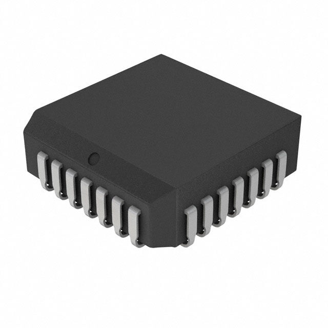
| 供应商器件封装 | 20-LFCSP-VQ(4x4) |
| 分频器/倍频器 | 是/是 |
| 包装 | 托盘 |
| 商标 | Analog Devices |
| 安装类型 | 表面贴装 |
| 安装风格 | SMD/SMT |
| 封装 | Tray |
| 封装/外壳 | 20-VFQFN 裸露焊盘,CSP |
| 封装/箱体 | LFCSP-20 |
| 工作温度 | -40°C ~ 85°C |
| 工作电源电压 | 3 V |
| 工厂包装数量 | 490 |
| 差分-输入:输出 | 是/无 |
| 最大工作温度 | + 85 C |
| 最大输入频率 | 6 GHz |
| 最小工作温度 | - 40 C |
| 最小输入频率 | 10 MHz |
| 标准包装 | 1 |
| 比率-输入:输出 | 2:1 |
| 电压-电源 | 2.7 V ~ 3.3 V |
| 电源电压-最大 | 3.3 V |
| 电源电压-最小 | 2.7 V |
| 电源电流 | 23 mA |
| 电路数 | 1 |
| 电路数量 | 1 |
| 类型 | Frac N |
| 系列 | ADF4157 |
| 输入 | CMOS,TTL |
| 输出 | 时钟 |
| 频率-最大值 | 6GHz |


- 商务部:美国ITC正式对集成电路等产品启动337调查
- 曝三星4nm工艺存在良率问题 高通将骁龙8 Gen1或转产台积电
- 太阳诱电将投资9.5亿元在常州建新厂生产MLCC 预计2023年完工
- 英特尔发布欧洲新工厂建设计划 深化IDM 2.0 战略
- 台积电先进制程称霸业界 有大客户加持明年业绩稳了
- 达到5530亿美元!SIA预计今年全球半导体销售额将创下新高
- 英特尔拟将自动驾驶子公司Mobileye上市 估值或超500亿美元
- 三星加码芯片和SET,合并消费电子和移动部门,撤换高东真等 CEO
- 三星电子宣布重大人事变动 还合并消费电子和移动部门
- 海关总署:前11个月进口集成电路产品价值2.52万亿元 增长14.8%


PDF Datasheet 数据手册内容提取
High Resolution 6 GHz Fractional-N Frequency Synthesizer Data Sheet ADF4157 FEATURES GENERAL DESCRIPTION RF bandwidth to 6 GHz The ADF4157 is a 6 GHz fractional-N frequency synthesizer with 25-bit fixed modulus allows subhertz frequency resolution a 25-bit fixed modulus, allowing subhertz frequency resolution 2.7 V to 3.3 V power supply at 6 GHz. It consists of a low noise digital phase frequency detector Separate V allows extended tuning voltage (PFD), a precision charge pump, and a programmable reference P Programmable charge pump currents divider. There is a Σ-Δ based fractional interpolator to allow 3-wire serial interface programmable fractional-N division. The INT and FRAC values Digital lock detect define an overall N divider, N = INT + (FRAC/225). The ADF4157 Power-down mode features cycle slip reduction circuitry, which leads to faster lock Pin compatible with the following frequency synthesizers: times without the need for modifications to the loop filter. ADF4110/ADF4111/ADF4112/ADF4113/ Control of all on-chip registers is via a simple 3-wire interface. ADF4106/ADF4153/ADF4154/ADF4156 The device operates with a power supply ranging from 2.7 V to Cycle slip reduction for faster lock times 3.3 V and can be powered down when not in use. APPLICATIONS Satellite communications terminals, radar equipment Instrumentation equipment Personal mobile radio (PMR) Base stations for mobile radio Wireless handsets FUNCTIONAL BLOCK DIAGRAM AVDD DVDD VP RSET ADF4157 5-BIT REFERENCE REFIN DOU×B2LER R COUNTER ÷2 DIVIDER + PHASE FREQUENCY CHARGE CP VDD –DETECTOR PUMP HIGH Z DGND CSR LOCK CURRENT DETECT SETTING MUXOUT OUMTUPXUT SDOUT VDD RFCP4RFCP3RFCP2RFCP1 RDIV RFINA NDIV N COUNTER RFINB THIRD-ORDER FRACTIONAL CE INTERPOLATOR CLK 32-BIT FRACTION MODULUS INTEGER DATA DATA REG 225 REG LE REGISTER AGND DGND CPGND 05874-001 Figure 1. Rev. D Information furnished by Analog Devices is believed to be accurate and reliable. However, no responsibility is assumed by Analog Devices for its use, nor for any infringements of patents or other One Technology Way, P.O. Box 9106, Norwood, MA 02062-9106, U.S.A. rights of third parties that may result from its use. Specifications subject to change without notice. No license is granted by implication or otherwise under any patent or patent rights of Analog Devices. Tel: 781.329.4700 www.analog.com Trademarks and registered trademarks are the property of their respective owners. Fax: 781.461.3113 ©2007–2012 Analog Devices, Inc. All rights reserved.
ADF4157 Data Sheet TABLE OF CONTENTS Features .............................................................................................. 1 Program Modes .......................................................................... 10 Applications ....................................................................................... 1 Register Maps .................................................................................. 11 General Description ......................................................................... 1 FRAC/INT Register (R0) Map.................................................. 12 Functional Block Diagram .............................................................. 1 LSB FRAC Register (R1) Map .................................................. 13 Revision History ............................................................................... 2 R Divider Register (R2) Map .................................................... 14 Specifications ..................................................................................... 3 Function Register (R3) Map ..................................................... 16 Timing Specifications .................................................................. 4 Test Register (R4) Map .............................................................. 17 Absolute Maximum Ratings ............................................................ 5 Applications Information .............................................................. 18 Thermal Resistance ...................................................................... 5 Initialization Sequence .............................................................. 18 ESD Caution .................................................................................. 5 RF Synthesizer: A Worked Example ........................................ 18 Pin Configurations and Function Descriptions ........................... 6 Reference Doubler and Reference Divider ............................. 18 Typical Performance Characteristics ............................................. 8 Cycle Slip Reduction for Faster Lock Times ........................... 18 Circuit Description ........................................................................... 9 Fastlock Timer and Register Sequences .................................. 19 Reference Input Section ............................................................... 9 Fastlock: An Example ................................................................ 19 RF Input Stage ............................................................................... 9 Fastlock: Loop Filter Topology ................................................. 19 RF INT Divider ............................................................................. 9 Spur Mechanisms ....................................................................... 19 25-Bit Fixed Modulus .................................................................. 9 Low Frequency Applications .................................................... 20 INT, FRAC, and R Relationship ................................................. 9 Filter Design—ADIsimPLL ....................................................... 20 RF R Counter ................................................................................ 9 Operating with Wide Loop Filter Bandwidths ....................... 20 Phase Frequency Detector (PFD) and Charge Pump ............ 10 PCB Design Guidelines for the Chip Scale Package .............. 20 MUXOUT and Lock Detect ...................................................... 10 Outline Dimensions ....................................................................... 21 Input Shift Register..................................................................... 10 Ordering Guide .......................................................................... 21 REVISION HISTORY 8/12—Rev. C to Rev. D Changes to Figure 4 and Table 5 ...................................................... 6 Changes to Figure 15 ...................................................................... 10 Changes to Figure 4 and Table 5 ...................................................... 6 Changes to Figure 16 ...................................................................... 11 Updated Outline Dimensions (Changed CP-20-1 to CP-20-6) ..... 22 Changes to Figure 17 ...................................................................... 12 Changes to Ordering Guide ........................................................... 21 Changes to Figure 19 ...................................................................... 15 Criticizing Added Negative Bleed Current Section, CLK Divider Mode 3/12—Rev. B to Rev. C Section, and 12-Bit Clock Divider Value Section....................... 17 Changes to Reserved Bits Section and Figure 21 ....................... 17 Changes to Table 1 ............................................................................ 3 Deleted Interfacing Section ........................................................... 18 Changes to Ordering Guide .......................................................... 21 Added Fastlock Timer and Register Sequences Section, 9/11—Rev. A to Rev. B Fastlock: An Example Section, and Fastlock: Loop Filter Changes to Noise Characteristics Parameter ................................ 3 Topology Section ............................................................................ 19 Changes to EPAD Note .................................................................... 6 Added Figure 22 and Figure 23; Renumbered Sequentially ..... 19 Added Operating with Wide Loop Filter Bandwidths 1/09—Rev. 0 to Rev. A Section .............................................................................................. 20 Changes to Figure 1 .......................................................................... 1 Updated Outline Dimensions ....................................................... 21 Changes to Reference Characteristics Parameter, Table 1 .......... 3 7/07—Revision 0: Initial Version Changes to Table 3 ............................................................................ 5 Rev. D | Page 2 of 24
Data Sheet ADF4157 SPECIFICATIONS AV = DV = 2.7 V to 3.3 V; V = AV to 5.5 V; AGND = DGND = 0 V; T = T to T , unless otherwise noted; DD DD P DD A MIN MAX dBm referred to 50 Ω. Table 1. Parameter B Version1 Unit Test Conditions/Comments RF CHARACTERISTICS (3 V) RF Input Frequency (RF ) 0.5/6.0 GHz min/max −10 dBm/0 dBm min/max; for lower frequencies, ensure slew rate IN (SR) > 400 V/µs REFERENCE CHARACTERISTICS REF Input Frequency 10/300 MHz min/max For f < 10 MHz, ensure slew rate > 50 V/µs IN REFIN REF Input Sensitivity 0.4/AV V p-p min/max For 10 MHz < f < 250 MHz, biased at AV /22 IN DD REFIN DD 0.7/AV V p-p min/max For 250 MHz < f < 300 MHz, biased at AV /22 DD REFIN DD REF Input Capacitance 10 pF max IN REF Input Current ±100 µA max IN PHASE DETECTOR Phase Detector Frequency3 32 MHz max CHARGE PUMP I Sink/Source Programmable CP High Value 5 mA typ With R = 5.1 kΩ SET Low Value 312.5 µA typ Absolute Accuracy 2.5 % typ With R = 5.1 kΩ SET R Range 2.7/10 kΩ min/max SET I Three-State Leakage Current 1 nA typ Sink and source current CP Matching 2 % typ 0.5 V < V < V – 0.5 CP P I vs. V 2 % typ 0.5 V < V < V – 0.5 CP CP CP P I vs. Temperature 2 % typ V = V/2 CP CP P LOGIC INPUTS V , Input High Voltage 1.4 V min INH V , Input Low Voltage 0.6 V max INL I /I , Input Current ±1 µA max INH INL C , Input Capacitance 10 pF max IN LOGIC OUTPUTS V , Output High Voltage 1.4 V min Open-drain 1 kΩ pull-up to 1.8 V OH V , Output High Voltage VDD – 0.4 V min CMOS output chosen OH V , Output Low Voltage 0.4 V max I = 500 µA OL OL POWER SUPPLIES AV 2.7/3.3 V min/max DD DV AV DD DD V AV /5.5 V min/V max P DD I 29 mA max 23 mA typical DD Low Power Sleep Mode 10 µA typ NOISE CHARACTERISTICS Normalized Phase Noise Floor −211 dBc/Hz typ PLL loop B/W = 500 kHz; (PN )4 measured at 100 kHz SYNTH Normalized 1/f Noise (PN )5 −110 dBc/Hz typ 10 kHz offset; normalized to 1 GHz 1_f Phase Noise Floor6 −137 dBc/Hz typ @ 10 MHz PFD frequency −133 dBc/Hz typ @ 25 MHz PFD frequency Phase Noise Performance7 @ VCO output 5800 MHz Output8 −87 dBc/Hz typ @ 2 kHz offset, 25 MHz PFD frequency 1 Operating temperature of B version is −40°C to +85°C. 2 AC-coupling ensures AV /2 bias. DD 3 Guaranteed by design. Sample tested to ensure compliance. 4 The synthesizer phase noise floor is estimated by measuring the in-band phase noise at the output of the VCO and subtracting 20 log(N) (where N is the N divider value) and 10 log(F ). PN = PN − 10 log(F ) − 20 log(N). PFD SYNTH TOT PFD 5 The PLL phase noise is composed of 1/f (flicker) noise plus the normalized PLL noise floor. The formula for calculating the 1/f noise contribution at an RF frequency, F , RF and at a frequency offset f is given by PN = PN + 10 log(10 kHz/f) + 20 log(F /1 GHz). Both the normalized phase noise floor and flicker noise are modeled in ADIsimPLL. 1_f RF 6 The synthesizer phase noise floor is estimated by measuring the in-band phase noise at the output of the VCO and subtracting 20logN (where N is the N divider value). 7 The phase noise is measured with the EV-ADF4157SD1Z and the Agilent E5052A phase noise system. 8 f = 100 MHz; f = 25 MHz; offset frequency = 2 kHz; RF = 5800.25 MHz; N = 232; loop bandwidth = 20 kHz. REFIN PFD OUT Rev. D | Page 3 of 24
ADF4157 Data Sheet TIMING SPECIFICATIONS AV = DV = 2.7 V to 3.3 V; V = AV to 5.5 V; AGND = DGND = 0 V; T = T to T , unless otherwise noted; DD DD P DD A MIN MAX dBm referred to 50 Ω. Table 2. Parameter Limit at T to T (B Version) Unit Test Conditions/Comments MIN MAX t 20 ns min LE setup time 1 t 10 ns min Data to clock setup time 2 t 10 ns min Data to clock hold time 3 t 25 ns min Clock high duration 4 t 25 ns min Clock low duration 5 t 10 ns min Clock to LE setup time 6 t 20 ns min LE pulse width 7 t4 t5 CLK t2 t3 DB2 DB1 DB0 (LSB) DATA DB23 (MSB) DB22 (CONTROL BIT C3) (CONTROL BIT C2) (CONTROL BIT C1) t7 LE t1 t6 LE 05874-002 Figure 2. Timing Diagram Rev. D | Page 4 of 24
Data Sheet ADF4157 ABSOLUTE MAXIMUM RATINGS T = 25°C, GND = AGND = DGND = 0 V, V = AV = DV , unless otherwise noted. A DD DD DD Table 3. THERMAL RESISTANCE Parameter Rating θ is specified for the worst-case conditions, that is, a device AV /DV to AGND/DGND −0.3 V to +4 V JA DD DD soldered in a circuit board for surface-mount packages. AV to DV −0.3 V to +0.3 V DD DD V to AGND/DGND −0.3 V to +5.8 V P Table 4. Thermal Resistance V to AV /DV −0.3 V to +5.8 V P DD DD Package Type θ Unit JA Digital I/O Voltage to AGND/DGND −0.3 V to V + 0.3 V DD TSSOP 112 °C/W Analog I/O Voltage to AGND/DGND −0.3 V to V + 0.3 V DD LFCSP (Paddle Soldered) 30.4 °C/W REF , RF x to AGND/DGND −0.3 V to V + 0.3 V IN IN DD Operating Temperature Range ESD CAUTION Industrial (B Version) −40°C to +85°C Storage Temperature Range −65°C to +125°C Maximum Junction Temperature 150°C Reflow Soldering Peak Temperature 260°C Time at Peak Temperature 40 sec Stresses above those listed under Absolute Maximum Ratings may cause permanent damage to the device. This is a stress rating only; functional operation of the device at these or any other conditions above those indicated in the operational section of this specification is not implied. Exposure to absolute maximum rating conditions for extended periods may affect device reliability. Rev. D | Page 5 of 24
ADF4157 Data Sheet PIN CONFIGURATIONS AND FUNCTION DESCRIPTIONS PC RTESVPVDDDVDDD 0 9 8 7 6 2 1 1 1 1 CPGND1 15MUXOUT AGND2 ADF4157 14LE RSET 1 16 VP AGND3 TOP VIEW 13DATA (Not to Scale) CP 2 15 DVDD RFINB4 12CLK CPGND 3 ADF4157 14 MUXOUT RFINA5 11CE AGND 4 TOP VIEW 13 LE (Not to Scale) 6 7 8 9 0 1 RRFFIINNAB 56 1121 CDLAKTA VADDVADDFERNIDNGD DNGD NOTES AVDD 7 10 CE 1. IT IS RECOMMENDED THAT THE EXPOSED PAD REFIN 8 9 DGND 05874-003 BPTHLEAI STNH PEEA FRDOM SRAH LEOLNUYH LCADON BCNEEN DEC COTTHNEENDRE MTCOTAE LAD PC TEOORP FAPOGERRNMDA.NCE. 05874-004 Figure 3. TSSOP Pin Configuration Figure 4. LFCSP Pin Configuration Table 5. Pin Function Descriptions TSSOP LFCSP Pin No. Pin No. Mnemonic Description 1 19 R Connecting a resistor between this pin and ground sets the maximum charge pump output SET current. The relationship between I and R is CP SET 25.5 I CPMAX R SET where: R = 5.1 kΩ. SET I = 5 mA. CPMAX 2 20 CP Charge Pump Output. When enabled, this pin provides ±I to the external loop filter, which, in CP turn, drives the external VCO. 3 1 CPGND Charge Pump Ground. This is the ground return path for the charge pump. 4 2, 3 AGND Analog Ground. This is the ground return path of the prescaler. 5 4 RF B Complementary Input to the RF Prescaler. This point should be decoupled to the ground plane IN with a small bypass capacitor, typically 100 pF. 6 5 RF A Input to the RF Prescaler. This small-signal input is normally ac-coupled from the VCO. IN 7 6, 7 AV Positive Power Supply for the RF Section. Decoupling capacitors to the digital ground plane DD should be placed as close as possible to this pin. AV has a value of 3 V ± 10%. AV must have DD DD the same voltage as DV . DD 8 8 REF Reference Input. This is a CMOS input with a nominal threshold of V /2 and an equivalent IN DD input resistance of 100 kΩ. This input can be driven from a TTL or CMOS crystal oscillator, or it can be ac-coupled. 9 9, 10 DGND Digital Ground. 10 11 CE Chip Enable. A logic low on this pin powers down the device and puts the charge pump output into three-state mode. 11 12 CLK Serial Clock Input. This serial clock is used to clock in the serial data to the registers. The data is latched into the input shift register on the CLK rising edge. This input is a high impedance CMOS input. 12 13 DATA Serial Data Input. The serial data is loaded MSB first with the three LSBs being the control bits. This input is a high impedance CMOS input. 13 14 LE Load Enable, CMOS Input. When LE is high, the data stored in the input shift register is loaded into one of the five latches, with the latch selected using the control bits. 14 15 MUXOUT This multiplexer output allows the lock detect, the scaled RF, or the scaled reference frequency to be accessed externally. Rev. D | Page 6 of 24
Data Sheet ADF4157 TSSOP LFCSP Pin No. Pin No. Mnemonic Description 15 16, 17 DV Positive Power Supply for the Digital Section. Decoupling capacitors to the digital ground DD plane should be placed as close as possible to this pin. DV has a value of 3 V ± 10%. DV DD DD must have the same voltage as AV . DD 16 18 V Charge Pump Power Supply. This should be greater than or equal to V . In systems where V P DD DD is 3 V, it can be set to 5.5 V and used to drive a VCO with a tuning range of up to 5.5 V. N/A 21 (EPAD) Exposed Pad It is recommended that the exposed pad be thermally connected to a copper plane for (EPAD) enhanced thermal performance. The pad should be connected to AGND. Rev. D | Page 7 of 24
ADF4157 Data Sheet TYPICAL PERFORMANCE CHARACTERISTICS PFD = 25 MHz, loop bandwidth = 20 kHz, reference = 100 MHz, I = 313 μA, phase noise measurements taken on the Agilent E5052A CP phase noise system. 10 6.00 5 5.95 0 CSR ON R (dBm) ––11–055 P = 4/5 P = 8/9 NCY (GHz)55..9805 E E CSR OFF POW –20 REQU5.80 F –25 5.75 –30 5.70 ––3450 05874-016 5.65 05874-019 0 1 2 3 4 5 6 7 8 9 –100 0 100 200 300 400 500 600 700 800 900 FREQUENCY (GHz) TIME (µs) Figure 5. RF Input Sensitivity Figure 8. Lock Time for 200 MHz Jump from 5705 MHz to 5905 MHz with CSR On and Off 0 5.95 VDD = 3V –5 5.90 –10 5.85 m) –15 GHz) CSR OFF dB Y (5.80 R ( –20 NC E E OW QU5.75 P –25 RE F 5.70 –30 CSR ON 5.65 ––3450 05874-017 5.60 05874-020 0 100 200 300 400 500 –100 0 100 200 300 400 500 600 700 800 900 FREQUENCY (MHz) TIME (µs) Figure 6. Reference Input Sensitivity Figure 9. Lock Time for 200 MHz Jump from 5905 MHz to 5705 MHz with CSR On and Off 0 6 RF = 5800.25MHz, PFD = 25MHz, N = 232, FRAC = 335544, FREQUENCY RESOLUTION = 0.74Hz, –20 20kHz LOOP BW, ICP = 313µA, DSB INTEGRATED PHASE 4 ERROR = 0.97° RMS, PHASE NOISE @ 2kHz = –87dBc/Hz. –40 Bc/Hz) –60 2 E (d mA) OIS –80 (P 0 E N IC S–100 A –2 H P –120 –4 ––114600 05874-018 –6 05874-021 1k 10k 100k 1M 10M 0 0.5 1.0 1.5 2.0 2.5 3.0 3.5 4.0 4.5 5.0 FREQUENCY (Hz) VCP (V) Figure 7. Phase Noise and Spurs Figure 10. Charge Pump Output Characteristics, Pump Up and Pump Down (Note that the 250 kHz spur is an integer boundary spur; see the Spur Mechanisms section for more information.) Rev. D | Page 8 of 24
Data Sheet ADF4157 CIRCUIT DESCRIPTION REFERENCE INPUT SECTION INT, FRAC, AND R RELATIONSHIP The reference input stage is shown in Figure 11. SW1 and SW2 The INT and FRAC values, in conjunction with the R counter, are normally closed switches. SW3 is normally open. When make it possible to generate output frequencies that are spaced power-down is initiated, SW3 is closed and SW1 and SW2 are by fractions of the phase frequency detector (PFD). See the RF open. This ensures that there is no loading of the REF pin on Synthesizer: A Worked Example section for more information. IN power-down. The RF VCO frequency (RF ) equation is OUT POWER-DOWN RF = f × (INT + (FRAC/225)) (1) CONTROL OUT PFD where: NC 100kΩ RF is the output frequency of the external voltage controlled OUT SW2 oscillator (VCO). REFIN NC TO R COUNTER BUFFER INT is the preset divide ratio of the binary 12-bit counter (23 to SW1 NC SW3 05874-005 4F0R9A5C). is the numerator of the fractional division (0 to 225 − 1). Figure 11. Reference Input Stage f = REF × [(1 + D)/(R × (1 + T))] (2) PFD IN RF INPUT STAGE where: The RF input stage is shown in Figure 12. It is followed by REF is the reference input frequency. IN a two-stage limiting amplifier to generate the current mode D is the REF doubler bit. IN logic (CML) clock levels needed for the prescaler. R is the preset divide ratio of the binary 5-bit programmable reference counter (1 to 32). BIAS 1.6V T is the REF divide-by-2 bit (0 or 1). GENERATOR IN AVDD RF R COUNTER 2kΩ 2kΩ The 5-bit RF R counter allows the input reference frequency (REF ) to be divided down to produce the reference clock to IN the PFD. Division ratios from 1 to 32 are allowed. RFINA RF N DIVIDER N = INT + FRAC/MOD FROM RF RFINB INPUT STAGE N-COUNTER TO PFD THIRD-ORDER FRACTIONAL INTERPOLATOR AGND 05874-006 INT MOD FRAC Figure 12. RF Input Stage REG REG VALUE RF INT DIVIDER 05874-007 The RF INT counter allows a division ratio in the PLL feedback Figure 13. RF N Divider counter. Division ratios from 23 to 4095 are allowed. 25-BIT FIXED MODULUS The ADF4157 has a 25-bit fixed modulus. This allows output frequencies to be spaced with a resolution of f = f /225 RES PFD where f is the frequency of the phase frequency detector PFD (PFD). For example, with a PFD frequency of 10 MHz, frequency steps of 0.298 Hz are possible. Rev. D | Page 9 of 24
ADF4157 Data Sheet PHASE FREQUENCY DETECTOR (PFD) AND INPUT SHIFT REGISTER CHARGE PUMP The ADF4157 digital section includes a 5-bit RF R counter, a The PFD takes inputs from the R counter and the N counter 12-bit RF N counter, and a 25-bit FRAC counter. Data is clocked and produces an output proportional to the phase and fre- into the 32-bit input shift register on each rising edge of CLK. quency difference between them. Figure 14 is a simplified The data is clocked in MSB first. Data is transferred from the schematic of the phase frequency detector. The PFD includes input shift register to one of five latches on the rising edge of a fixed delay element that sets the width of the antibacklash LE. The destination latch is determined by the state of the three pulse, which is typically 3 ns. This pulse ensures that there is no control bits (C3, C2, and C1) in the input shift register. These dead zone in the PFD transfer function and gives a consistent are the three LSBs, DB2, DB1, and DB0, as shown in Figure 2. reference spur level. The truth table for these bits is shown in Table 6. Figure 16 shows a summary of how the latches are programmed. UP HI D1 Q1 U1 PROGRAM MODES +IN CLR1 Table 6 and Figure 16 through Figure 21 show how to set up the program modes in the ADF4157. DELAY U3 CHPUAMRGPE CP Several settings in the ADF4157 are double-buffered. These include the LSB FRAC value, R counter value, reference doubler, and current setting. This means that two events have to occur CLR2 DOWN before the part uses a new value of any of the double-buffered HI D2 Q2 settings. First, the new value is latched into the device by writing to –IN U2 05874-008 tohne Raepgpirsoteprr i0a,t eR 0re. g ister. Second, a new write must be performed Figure 14. PFD Simplified Schematic For example, updating the fractional value can involve a write MUXOUT AND LOCK DETECT to the 13 LSB bits in R1 and the 12 MSB bits in R0. R1 should The output multiplexer on the ADF4157 allows the user to access be written to first, followed by the write to R0. The frequency various internal points on the chip. The state of MUXOUT is change begins after the write to R0. Double buffering ensures controlled by M4, M3, M2, and M1 (see Figure 17). Figure 15 that the bits written to in R1 do not take effect until after the shows the MUXOUT section in block diagram form. write to R0. Table 6. C3, C2, and C1 Truth Table THREE-STATE OUTPUT DVDD Control Bits DVDD C3 C2 C1 Register DGND 0 0 0 Register 0 (R0) R DIVIDER OUTPUT 0 0 1 Register 1 (R1) N DIVIDER OUTPUT 0 1 0 Register 2 (R2) ANALOG LOCK DETECT MUX CONTROL MUXOUT 0 1 1 Register 3 (R3) DIGITAL LOCK DETECT 1 0 0 Register 4 (R4) SERIAL DATA OUTPUT CLK DIVIDER OUTPUT FASTLOCK SWITCH NR DDIIVVIIDDEERR//22 DGND 05874-009 Figure 15. MUXOUT Schematic Rev. D | Page 10 of 24
Data Sheet ADF4157 REGISTER MAPS FRAC/INT REGISTER (R0) D E V SER CMOUNXTORUOTL 12-BIT INTEGER VALUE (INT) 12-BIT MSB F(RFARCATCI)ONAL VALUE COBNITTRSOL E R DB31DB30DB29DB28DB27DB26DB25DB24DB23DB22DB21DB20DB19DB18DB17DB16DB15DB14DB13DB12DB11DB10 DB9 DB8 DB7 DB6 DB5 DB4 DB3 DB2 DB1 DB0 0 M4 M3 M2 M1 N12 N11 N10 N9 N8 N7 N6 N5 N4 N3 N2 N1 F25 F24 F23 F22 F21 F20 F19 F18 F17 F16 F15 F14 C3(0)C2(0)C1(0) LSB FRAC REGISTER (R1) RESERVED 13-BIT LSB FRACTIONAL VALUE RESERVED CONTROL (FRAC) (DBB) BITS DB31DB30DB29DB28DB27DB26DB25DB24DB23DB22DB21DB20DB19DB18DB17DB16DB15DB14DB13DB12DB11DB10 DB9 DB8 DB7 DB6 DB5 DB4 DB3 DB2 DB1 DB0 0 0 0 0 F13 F12 F11 F10 F9 F8 F7 F6 F5 F4 F3 F2 F1 0 0 0 0 0 0 0 0 0 0 0 0 C3(0)C2(0)C1(1) R DIVIDER REGISTER (R2) DBB B DBB RESERVED RESERVED CSR EN CSUERTRTEINNGT RESERVED PRESCALER RDIV2 DBB REFERENCEOUBLER DB 5-BIT R COUNTER RESERVED COBNITTRSOL D DB31DB30DB29DB28DB27DB26DB25DB24DB23DB22DB21DB20DB19DB18DB17DB16DB15DB14DB13DB12DB11DB10 DB9 DB8 DB7 DB6 DB5 DB4 DB3 DB2 DB1 DB0 0 0 0 C1 CPI4 CPI3 CPI2 CPI1 0 P1 U2 U1 R5 R4 R3 R2 R1 0 0 0 0 0 0 0 0 0 0 0 0 C3(0)C2(1)C1(0) FUNCTION REGISTER (R3) E RESERVED SDRESET RESERVED LDP PDPOLARITY PD CPHREE-STATCOUNTERRESET COBNITTRSOL T DB31DB30DB29DB28DB27DB26DB25DB24DB23DB22DB21DB20DB19DB18DB17DB16DB15DB14DB13DB12DB11DB10 DB9 DB8 DB7 DB6 DB5 DB4 DB3 DB2 DB1 DB0 0 0 0 0 0 0 0 0 0 0 0 0 0 0 0 0 0 U12 0 0 0 0 0 0 U11 U10 U9 U8 U7 C3(0)C2(1)C1(1) TEST REGISTER (R4) RESERVED NEGBLEEDCURRENT RESERVED MCDOLIDVKE 12-BIT CLOCK DIVIDER VALUE RESERVED COBNITTRSOL DB31DB30DB29DB28DB27DB26DB25DB24DB23DB22DB21DB20DB19DB18DB17DB16DB15DB14DB13DB12DB11DB10 DB9 DB8 DB7 DB6 DB5 DB4 DB3 DB2 DB1 DB0 0 0 0 0 0 0 0 NB2 NB1 0 0 C2 C1 D12 D11 D10 D9 D8 D7 D6 D5 D4 D3 D2 D1 0 0 0 0 C3(1)C2(0)C1(0) N1.O DTBEBS = DOUBLE BUFFERED BIT(S). 05874-010 Figure 16. Register Summary Rev. D | Page 11 of 24
ADF4157 Data Sheet FRAC/INT REGISTER (R0) MAP in Equation 1. See the INT, FRAC, and R Relationship section for more information. With R0[2:0] set to 000, the on-chip FRAC/INT register is programmed as shown in Figure 17. 12-Bit MSB FRAC Value Reserved Bit These 12 bits, along with Bits DB[27:15] in the LSB FRAC register (R1), control what is loaded as the FRAC value into The reserved bit should be set to 0 for normal operation. the fractional interpolator. This is part of what determines the MUXOUT overall feedback division factor. It is also used in Equation 1. The on-chip multiplexer is controlled by Bits DB[30:27] on the These 12 bits are the most significant bits (MSB) of the 25-bit ADF4157. See Figure 17 for the truth table. FRAC value, and Bits DB[27:15] in the LSB FRAC register (R1) 12-Bit INT Value are the least significant bits (LSB). See the RF Synthesizer: A Worked Example section for more information. These 12 bits control what is loaded as the INT value. This is used to determine the overall feedback division factor. It is used D E V SER CMOUNXTORUOTL 12-BIT INTEGER VALUE (INT) 12-BIT MSB F(RFARCATCI)ONAL VALUE COBNITTRSOL E R DB31DB30DB29DB28DB27DB26DB25DB24DB23DB22DB21DB20DB19DB18DB17DB16DB15DB14DB13DB12DB11DB10 DB9 DB8 DB7 DB6 DB5 DB4 DB3 DB2 DB1 DB0 0 M4 M3 M2 M1 N12 N11 N10 N9 N8 N7 N6 N5 N4 N3 N2 N1 F25 F24 F23 F22 F21 F20 F19 F18 F17 F16 F15 F14 C3(0)C2(0)C1(0) M4 M3 M2 M1 OUTPUT MSB FRACTIONAL VALUE F12 F11 .......... F2 F1 (FRAC)* 0 0 0 0 THREE-STATE OUTPUT 0 0 .......... 0 0 0 0 0 0 1 DVDD 0 0 .......... 0 1 1 0 0 1 0 DGND 0 0 .......... 1 0 2 0 0 1 1 RDIVIDEROUTPUT 0 0 .......... 1 1 3 0 1 0 0 NDIVIDEROUTPUT . . .......... . . . 0 1 0 1 ANALOGLOCKDETECT . . .......... . . . 0 1 1 0 DIGITALLOCKDETECT . . .......... . . . 0 1 1 1 SERIALDATAOUTPUT 1 1 .......... 0 0 4092 1 0 0 0 RESERVED 1 1 .......... 0 1 4093 1 0 0 1 RESERVED 1 1 .......... 1 0 4094 1 0 1 0 CLKDIVIDER OUTPUT 1 1 .......... 1 1 4095 1 0 1 1 RESERVED 1 1 0 0 FASTLOCK SWITCH *THE FRAC VALUE IS MADE UP OF THE 12-BIT MSB STORED IN REGISTER 0, AND THE 13-BIT LSB REGISTER STORED IN 1 1 0 1 RDIVIDER/2 REGISTER 1. FRAC VALUE = 13-BIT LSB + 12-BIT MSB × 213. 1 1 1 0 NDIVIDER/2 1 1 1 1 RESERVED INTEGERVALUE N12 N11 N10 N9 N8 N7 N6 N5 N4 N3 N2 N1 (INT) 0 0 0 0 0 0 0 1 0 1 1 1 23 0 0 0 0 0 0 0 1 1 0 0 0 24 0 0 0 0 0 0 0 1 1 0 0 1 25 0 0 0 0 0 0 0 1 1 0 1 0 26 . . . . . . . . . . . . . . . . . . . . . . . . . . . . . . . . . . . . . . . 1 1 1 1 1 1 1 1 1 1 0 1 4093 11 11 11 11 11 11 11 11 11 11 11 01 44009945 05874-011 Figure 17. FRAC/INT Register (R0) Map Rev. D | Page 12 of 24
Data Sheet ADF4157 LSB FRAC REGISTER (R1) MAP These 13 bits are the least significant bits of the 25-bit FRAC value, and Bits DB[14:3] in the INT/FRAC register are the most With R1[2:0] set to 001, the on-chip LSB FRAC register is significant bits. See the RF Synthesizer: A Worked Example programmed as shown in Figure 18. section for more information. 13-Bit LSB FRAC Value Reserved Bits These 13 bits, along with Bits DB[14:3] in the INT/FRAC All reserved bits should be set to 0 for normal operation. register (R0), control what is loaded as the FRAC value into the fractional interpolator. This is part of what determines the overall feedback division factor. It is also used in Equation 1. RESERVED 13-BIT LSB FRACTIONAL VALUE RESERVED CONTROL (FRAC) (DBB) BITS DB31DB30DB29DB28DB27DB26DB25DB24DB23DB22DB21DB20DB19DB18DB17DB16DB15DB14DB13DB12DB11DB10 DB9 DB8 DB7 DB6 DB5 DB4 DB3 DB2 DB1 DB0 0 0 0 0 F13 F12 F11 F10 F9 F8 F7 F6 F5 F4 F3 F2 F1 0 0 0 0 0 0 0 0 0 0 0 0 C3(0)C2(0)C1(1) LSB FRACTIONAL VALUE F25 F24 .......... F14 F13 (FRAC)* 0 0 .......... 0 0 0 0 0 .......... 0 1 1 0 0 .......... 1 0 2 0 0 .......... 1 1 3 . . .......... . . . . . .......... . . . . . .......... . . . 1 1 .......... 0 0 8188 1 1 .......... 0 1 8189 1 1 .......... 1 0 8190 1 1 .......... 1 1 8191 * RRTHEEGGE IIFSSRTTAEECRR V01,.A AFLRNUADEC TI SHV AEM LA1U3DE-EB =IUT 1P L3 OS-BBFIT RT LHESEGB I1S 2+T- B1E2RIT- B SMITTSO MBR SSEBTD O× I NR21E3D. IN 05874-012 Figure 18. LSB FRAC Register (R1) Map Rev. D | Page 13 of 24
ADF4157 Data Sheet R DIVIDER REGISTER (R2) MAP RDIV2 With R2[2:0] set to 010, the on-chip R divider register is Setting this bit to 1 inserts a divide-by-2 toggle flip-flop programmed as shown in Figure 19. between the R counter and the PFD. This can be used to provide a 50% duty cycle signal at the PFD for use with cycle CSR Enable slip reduction. Setting this bit to 1 enables cycle slip reduction. This is a Reference Doubler method for improving lock times. Note that the signal at the PFD must have a 50% duty cycle for cycle slip reduction to work. In Setting DB[20] to 0 feeds the REF signal directly to the 5-bit IN addition, the charge pump current setting must be set to a RF R counter, disabling the doubler. Setting this bit to 1 multiplies minimum. See the Cycle Slip Reduction for Faster Lock Times the REF frequency by a factor of 2 before feeding into the 5-bit IN section for more information. R counter. When the doubler is disabled, the REF falling edge IN is the active edge at the PFD input to the fractional synthesizer. Note also that the cycle slip reduction feature can only be When the doubler is enabled, both the rising edge and falling operated when the phase detector polarity setting is positive edge of REF become active edges at the PFD input. (DB6 in Register 3). It cannot be used if the phase detector IN polarity is set to negative. The maximum allowed REF frequency when the doubler is IN enabled is 30 MHz. Charge Pump Current Setting 5-Bit R Counter Bits DB[27:24] set the charge pump current setting. This should be set to the charge pump current that the loop filter is designed The 5-bit R counter allows the input reference frequency with (see Figure 19). (REF ) to be divided down to produce the reference clock to IN the phase frequency detector (PFD). Division ratios from Prescaler (P/P + 1) 1 to 32 are allowed. The dual-modulus prescaler (P/P + 1), along with INT, FRAC, Reserved Bits and MOD, determine the overall division ratio from RF x to IN the PFD input. All reserved bits should be set to 0 for normal operation. Operating at CML levels, it takes the clock from the RF input stage and divides it down for the counters. It is based on a synchronous 4/5 core. When set to 4/5, the maximum RF frequency allowed is 3 GHz. Therefore, when operating the ADF4157 above 3 GHz, the prescaler must be set to 8/9. The prescaler limits the INT value. With P = 4/5, N = 23. MIN With P = 8/9, N = 75. MIN Rev. D | Page 14 of 24
Data Sheet ADF4157 RESERVED RESERVED CSR EN CSUERTRTEINNGTDBB RESERVED PRESCALER RDIV2 DBB REFERENCEDOUBLER DBB 5-BIT R COUNTEDRBB RESERVED COBNITTRSOL DB31DB30DB29DB28DB27DB26DB25DB24DB23DB22DB21DB20DB19DB18DB17DB16DB15DB14DB13DB12DB11DB10 DB9 DB8 DB7 DB6 DB5 DB4 DB3 DB2 DB1 DB0 0 0 0 C1 CPI4 CPI3 CPI2 CPI1 0 P1 U2 U1 R5 R4 R3 R2 R1 0 0 0 0 0 0 0 0 0 0 0 0 C3(0)C2(1)C1(0) CYCLE SLIP REFERENCE C1 REDUCTION U1 DOUBLER 0 DISABLED 0 DISABLED 1 ENABLED 1 ENABLED U2 R DIVIDER 0 DISABLED 1 ENABLED P1 PRESCALER 0 4/5 1 8/9 ICP(mA) R5 R4 R3 R2 R1 RCOUNTERDIVIDERATIO CPI4 CPI3 CPI2 CPI1 5.1kΩ 0 0 0 0 1 1 0 0 0 0 0.31 0 0 0 1 0 2 0 0 0 1 0.63 0 0 0 1 1 3 0 0 1 0 0.94 0 0 1 0 0 4 0 0 1 1 1.25 . . . . . 0 1 0 0 1.57 . . . . . 0 1 0 1 1.88 . . . . . 0 1 1 0 2.19 1 1 1 0 1 29 0 1 1 1 2.5 1 1 1 1 . 30 1 0 0 0 2.81 1 1 1 1 1 31 1 0 0 1 3.13 0 0 0 0 0 32 1 0 1 0 3.44 1 0 1 1 3.75 1 1 0 0 4.06 1 1 0 1 4.38 11 11 11 01 45.69 05874-013 Figure 19. R Divider Register (R2) Map Rev. D | Page 15 of 24
ADF4157 Data Sheet FUNCTION REGISTER (R3) MAP RF Power-Down With R3[2:0] set to 011, the on-chip function register is DB[5] provides the programmable power-down mode. Setting programmed as shown in Figure 20. this bit to 1 performs a power-down. Setting this bit to 0 returns the synthesizer to normal operation. While in software power- Reserved Bits down mode, the part retains all information in its registers. All reserved bits should be set to 0 for normal operation. Only when supplies are removed are the register contents lost. Σ-Δ Reset When a power-down is activated, the following events occur: For most applications, DB14 should be set to 0. When DB14 is • All active dc current paths are removed. set to 0, the Σ-Δ modulator is reset on each write to Register 0. • The synthesizer counters are forced to their load state If it is not required that the Σ-Δ modulator be reset on each conditions. Register 0 write, this bit should be set to 1. • The charge pump is forced into three-state mode. Lock Detect Precision (LDP) • The digital lock detect circuitry is reset. When DB[7] is programmed to 0, 24 consecutive PFD cycles of • The RF x input is debiased. IN 15 ns must occur before digital lock detect is set. When this bit • The input shift register remains active and capable of is programmed to 1, 40 consecutive reference cycles of 15 ns loading and latching data. must occur before digital lock detect is set. RF Charge Pump Three-State Phase Detector Polarity DB[4] puts the charge pump into three-state mode when DB[6] sets the phase detector polarity. When the VCO programmed to 1. It should be set to 0 for normal operation. characteristics are positive, this should be set to 1. When they RF Counter Reset are negative, it should be set to 0. DB[3] is the RF counter reset bit for the ADF4157. When this is 1, the RF synthesizer counters are held in reset. For normal operation, this bit should be 0. E RESERVED SDRESET RESERVED LDP PDPOLARITY PD CPHREE-STATCOUNTERRESET COBNITTRSOL T DB31DB30DB29DB28DB27DB26DB25DB24DB23DB22DB21DB20DB19DB18DB17DB16DB15DB14DB13DB12DB11DB10 DB9 DB8 DB7 DB6 DB5 DB4 DB3 DB2 DB1 DB0 0 0 0 0 0 0 0 0 0 0 0 0 0 0 0 0 0 U12 0 0 0 0 0 0 U11 U10 U9 U8 U7 C3(0)C2(1)C1(1) COUNTER U11 LDP U7 RESET 0 24PFDCYCLES 0 DISABLED 1 40PFDCYCLES 1 ENABLED U12 SD RESET 0 ENABLED 1 DISABLED CP U10 PDPOLARITY U8 THREE-STATE 0 NEGATIVE 0 DISABLED 1 POSITIVE 1 ENABLED U9 POWER-DOWN 01 DENISAABBLLEEDD 05874-014 Figure 20. Function Register (R3) Map Rev. D | Page 16 of 24
Data Sheet ADF4157 TEST REGISTER (R4) MAP CLK Divider Mode With R4[2:0] set to 100, the on-chip test register (R4) is Setting Bits DB[20:19] to 01 enables switched R fastlock. programmed as shown in Figure 21. 12-Bit Clock Divider Value Negative Bleed Current Bits DB[18:7] are used to program the clock divider, which Setting Bits DB[24:23] to 11 turns on the constant negative determines for how long the loop remains in wideband mode bleed current. This ensures that the charge pump operates out while the switched R fastlock technique is used. of the dead zone. Thus the phase noise is not degraded and the Reserved Bits level of spurs is lower. Enabling constant negative bleed current All reserved bits should be set to 0 for normal operation. is particularly important on channels close to multiple PFD frequencies. D BNLEEGED RVE CLK CONTROL RESERVED CEUNRTR- ESE MDOIDVE 12-BIT CLOCK DIVIDER VALUE RESERVED BITS R DB31DB30DB29DB28DB27DB26DB25DB24DB23DB22DB21DB20DB19DB18DB17DB16DB15DB14DB13DB12DB11DB10 DB9 DB8 DB7 DB6 DB5 DB4 DB3 DB2 DB1 DB0 0 0 0 0 0 0 0 NB2 NB1 0 0 C2 C1 D12 D11 D10 D9 D8 D7 D6 D5 D4 D3 D2 D1 0 0 0 0 C3(1)C2(0)C1(0) NB2 NB1 NEGATIVE BLEED CURRENT D12 D11 .......... D2 D1 CLOCK DIVIDER VALUE 0 0 OFF 0 0 .......... 0 0 0 1 1 ON 0 0 .......... 0 1 1 0 0 .......... 1 0 2 0 0 .......... 1 1 3 . . .......... . . . . . .......... . . . . . .......... . . . 1 1 .......... 0 0 4092 C2 C1 CLOCK DIVIDER MODE 1 1 .......... 0 1 4093 00 01 CSWLOITCCKHDEIDV IRD EFRASOTFLFOCK ENABLE 11 11 .................... 11 01 44009945 05874-015 Figure 21. Test Register (R4) Map Rev. D | Page 17 of 24
ADF4157 Data Sheet APPLICATIONS INFORMATION INITIALIZATION SEQUENCE note that the PFD cannot be operated above 32 MHz due to a limitation in the speed of the Σ-Δ circuit of the N divider. After powering up the part, this programming sequence must be followed: CYCLE SLIP REDUCTION FOR FASTER LOCK TIMES 1. Test register (R4) In fastlocking applications, a wide loop filter bandwidth is 2. Function register (R3) required for fast frequency acquisition, resulting in increased 3. R divider register (R2) integrated phase noise and reduced spur attenuation. Using 4. LSB FRAC register (R1) cycle slip reduction, the loop bandwidth can be kept narrow to 5. FRAC/INT register (R0) reduce integrated phase noise and attenuate spurs while still realizing fast lock times. RF SYNTHESIZER: A WORKED EXAMPLE Cycle Slips The following equation governs how the synthesizer should be Cycle slips occur in integer-N/fractional-N synthesizers when programmed: the loop bandwidth is narrow compared to the PFD frequency. RF = [N + (FRAC/225)] × [f ] (3) OUT PFD The phase error at the PFD inputs accumulates too fast for the PLL where: to correct, and the charge pump temporarily pumps in the wrong RF is the RF frequency output. direction, slowing down the lock time dramatically. The ADF4157 OUT N is the integer division factor. contains a cycle slip reduction circuit to extend the linear range FRAC is the fractionality. of the PFD, allowing faster lock times without loop filter changes. f = REF × [(1 + D)/(R × (1 + T))] (4) When the ADF4157 detects that a cycle slip is about to occur, it PFD IN turns on an extra charge pump current cell. This outputs a constant where: current to the loop filter or removes a constant current from the REF is the reference frequency input. IN loop filter (depending on whether the VCO tuning voltage needs D is the RF REF doubler bit. IN to increase or decrease to acquire the new frequency). The effect is R is the RF reference division factor. that the linear range of the PFD is increased. Stability is main- T is the reference divide-by-2 bit (0 or 1). tained because the current is constant and is not a pulsed current. For example, in a system where a 5.8002 GHz RF frequency If the phase error increases again to a point where another cycle output (RF ) is required and a 10 MHz reference frequency OUT slip is likely, the ADF4157 turns on another charge pump cell. input (REF ) is available, the frequency resolution is IN This continues until the ADF4157 detects that the VCO frequency f = REF /225 RES IN has exceeded the desired frequency. It then begins to turn off f = 10 MHz/225 = 0.298 Hz RES the extra charge pump cells one by one until they are all turned From Equation 4, off and the frequency is settled. f = [10 MHz × (1 + 0)/1] = 10 MHz Up to seven extra charge pump cells can be turned on. In most PFD 5.8002 GHz = 10 MHz × (N + FRAC/225) applications, it is enough to eliminate cycle slips altogether, giving much faster lock times. Calculating N and FRAC values, Setting Bit DB28 in the R Divider register (R2) to 1 enables cycle N = int(RF /f ) = 580 OUT PFD FRAC = F × 213 + F slip reduction. Note that a 45% to 55% duty cycle is needed on MSB LSB F = int(((RF /f ) − N) × 212) = 81 the signal at the PFD for CSR to operate correctly. The reference MSB OUT PFD F = int(((((RF /f ) − N) × 212) − F ) × 213) = 7537 divide-by-2 flip-flop can help to provide a 50% duty cycle at the LSB OUT PFD MSB PFD. For example, if a 100 MHz reference frequency is available, where: and the user wants to run the PFD at 10 MHz, setting the R divide F is the 12-bit MSB FRAC value in Register R0. MSB factor to 10 results in a 10 MHz PFD signal that is not 50% duty F is the 13-bit LSB FRAC value in Register R1. LSB cycle. By setting the R divide factor to 5 and enabling the reference int() makes an integer of the argument in brackets. divide-by-2 bit, a 50% duty cycle 10 MHz signal can be achieved. REFERENCE DOUBLER AND REFERENCE DIVIDER Note that the cycle slip reduction feature can only be operated The on-chip reference doubler allows the input reference signal when the phase detector polarity setting is positive (DB6 in to be doubled. This is useful for increasing the PFD comparison Register 3). It cannot be used if the phase detector polarity is frequency. Making the PFD frequency higher improves the noise set to negative. performance of the system. Doubling the PFD frequency usually improves noise performance by 3 dB. It is important to Rev. D | Page 18 of 24
Data Sheet ADF4157 FASTLOCK TIMER AND REGISTER SEQUENCES ADF4157 R2 CP VCO If the fastlock mode is used, a timer value needs to be loaded into C1 C2 C3 the PLL to determine the time spent in wide bandwidth mode. When Bits DB[20:19] in Register 4 (R4) are set to 01 (switched R1A R1 MUXOUT R fastlock enable), the timer value is loaded via the 12-bit clock divider value. To use fastlock, the PLL must be written to in the 05874-023 following sequence: Figure 23. Fastlock Loop Filter Topology—Topology 2 1. Use the initialization sequence (see the Initialization SPUR MECHANISMS Sequence section) only once after powering up the part. The fractional interpolator in the ADF4157 is a third-order Σ-Δ 2. Load Register 4 (R4) with Bits DB[20:19] set to 01 and the modulator (SDM) with a 25-bit fixed modulus (MOD). The chosen fastlock timer value (DB18 to DB7). Note that the SDM is clocked at the PFD reference rate (f ) that allows PLL duration that the PLL remains in wide bandwidth is equal PFD output frequencies to be synthesized at a channel step resolution of to the fastlock timer/f . PFD f /MOD. The various spur mechanisms possible with fractional- PFD FASTLOCK: AN EXAMPLE N synthesizers, and how they affect the ADF4157, are discussed in this section. If a PLL has f = 13 MHz and a required lock time of 50 µs, PFD the PLL is set to wide bandwidth for 40 µs. Fractional Spurs If the time period set for the wide bandwidth is 40 µs, then In most fractional synthesizers, fractional spurs can appear at the set channel spacing of the synthesizer. In the ADF4157, Fastlock Timer Value = Time in Wide Bandwidth × f PFD these spurs do not appear. The high value of the fixed modulus Fastlock Timer Value = 40 µs × 13 MHz = 520 in the ADF4157 makes the Σ-Δ modulator quantization error Therefore, 520 must be loaded into the clock divider value in spectrum look like broadband noise, effectively spreading the Register 4 (R4) in Step 2 of the sequence described in the fractional spurs into noise. Fastlock Timer and Register Sequences section. Integer Boundary Spurs FASTLOCK: LOOP FILTER TOPOLOGY Interactions between the RF VCO frequency and the PFD fre- To use fast-lock mode, an extra connection from the PLL to the quency can lead to spurs known as integer boundary spurs. When loop filter is needed. The damping resistor in the loop filter must these frequencies are not integer related (which is the purpose be reduced to ¼ of its value while in wide bandwidth mode. This is of the fractional-N synthesizer), spur sidebands appear on the required because the charge pump current is increased by 16 VCO output spectrum at an offset frequency that corresponds while in wide bandwidth mode, and stability must be ensured. to the beat note or difference frequency between an integer mul- During fastlock, the MUXOUT pin (after setting MUXOUT to tiple of the PFD and the VCO frequency. fastlock switch by setting Bits DB[30:27] in Register 0 to 1100) is These spurs are named integer boundary spurs because they are shorted to ground (this is accomplished by settings Bits DB[20:19] more noticeable on channels close to integer multiples of the PFD in Register 4 to 01—switched R fastlock enable). The following where the difference frequency can be inside the loop bandwidth. two topologies can be used: These spurs are attenuated by the loop filter. • Divide the damping resistor (R1) into two values (R1 and Figure 7 shows an integer boundary spur. The RF frequency is R1A) that have a ratio of 1:3 (see Figure 22). 5800.25 MHz, and the PFD frequency is 25 MHz. The integer • Connect an extra resistor (R1A) directly from MUXOUT, boundary spur is 250 kHz from the carrier at an integer times as shown in Figure 23. The extra resistor must be chosen the PFD frequency (232 × 25 MHz = 5800 MHz). The spur also such that the parallel combination of an extra resistor and appears on the upper sideband. the damping resistor (R1) is reduced to ¼ of the original Reference Spurs value of R1 (see Figure 23). Reference spurs are generally not a problem in fractional-N ADF4157 R2 synthesizers because the reference offset is far outside the loop CP VCO bandwidth. However, any reference feedthrough mechanism C1 C2 C3 that bypasses the loop can cause a problem. One such mechanism R1 is the feedthrough of low levels of on-chip reference switching MUXOUT noise out through the RF x pin back to the VCO, resulting in R1A IN 05874-022 rthefee rPeCncBe lsapyuoru lte tvoe les nassu hrieg hth aast −th90e dVBCcO. C iasr we eshllo suelpda braet teadk efrno imn Figure 22. Fast-Lock Loop Filter Topology—Topology 1 the input reference to avoid a possible feedthrough path on the board. Rev. D | Page 19 of 24
ADF4157 Data Sheet LOW FREQUENCY APPLICATIONS PCB DESIGN GUIDELINES FOR THE CHIP SCALE PACKAGE The specification on the RF input is 0.5 GHz minimum; however, RF frequencies lower than this can be used, providing the mini- The lands on the chip scale package (CP-20) are rectangular. mum slew rate specification of 400 V/µs is met. An appropriate The printed circuit board pad for these should be 0.1 mm LVDS driver can be used to square up the RF signal before it is longer than the package land length and 0.05 mm wider than fed back to the ADF4157 RF input. The FIN1001 from Fairchild the package land width. The land should be centered on the pad. Semiconductor is one such LVDS driver. This ensures that the solder joint size is maximized. FILTER DESIGN—ADIsimPLL The bottom of the chip scale package has a central thermal pad. The thermal pad on the printed circuit board (PCB) should be A filter design and analysis program is available to help the user at least as large as the exposed pad. On the printed circuit implement PLL design. Visit www.analog.com/pll for a free board, there should be a clearance of at least 0.25 mm between download of the ADIsimPLL™ software. The software designs, the thermal pad and the inner edges of the pad pattern. This simulates, and analyzes the entire PLL frequency domain and ensures that shorting is avoided. time domain response. Various passive and active filter architec- tures are allowed. Thermal vias can be used on the PCB thermal pad to improve OPERATING WITH WIDE LOOP FILTER thermal performance of the package. If vias are used, they should be incorporated into the thermal pad at 1.2 mm pitch grid. The BANDWIDTHS via diameter should be between 0.3 mm and 0.33 mm, and the If a wide loop filter bandwidth is used (>60 kHz), fluctuations via barrel should be plated with 1 ounce of copper to plug the in the phase noise profile may be noticed on channels that are via. The user should connect the PCB thermal pad to AGND. close to integer multiples of the PFD frequency. This is due to operation of the charge pump close to the dead zone. To improve the phase noise, a bleed current can be enabled to bias the charge pump away from the dead zone. To enable this, set Bit DB[24:23] in Register 4. Using this mode has the added advantage of improving the integer boundary spurs by 4 dB to 5 dB. Note that it is also safe to use this mode if the loop filter bandwidth is <60 kHz. Rev. D | Page 20 of 24
Data Sheet ADF4157 OUTLINE DIMENSIONS 5.10 5.00 4.90 16 9 4.50 6.40 4.40 BSC 4.30 1 8 PIN 1 1.20 MAX 0.15 0.20 0.05 0.09 0.75 0.30 8° 0.60 B0.S6C5 0.19 SPELAANTIENG 0° 0.45 COPLANARITY 0.10 COMPLIANT TO JEDEC STANDARDS MO-153-AB Figure 24. 16-Lead Thin Shrink Small Outline Package [TSSOP] (RU-16) Dimensions shown in millimeters 4.10 0.30 4.00SQ 0.25 PIN1 3.90 0.18 INDICATOR PIN1 16 20 INDICATOR 0.50 BSC 15 1 EXPOSED 2.30 PAD 2.10SQ 2.00 11 5 0.65 10 6 0.20MIN TOPVIEW 0.60 BOTTOMVIEW 0.55 0.80 FORPROPERCONNECTIONOF 0.75 THEEXPOSEDPAD,REFERTO 0.05MAX THEPINCONFIGURATIONAND 0.70 0.02NOM FUNCTIONDESCRIPTIONS SECTIONOFTHISDATASHEET. COPLANARITY SEATING 0.08 PLANE COMPLIANTTOJED0E.2C0SRTEAFNDARDSMO-220-WGGD-1. 08-16-2010-B Figure 25. 20-Lead Lead Frame Chip Scale Package [LFCSP_WQ] 4mm × 4 mm Body, Very Very Thin Quad (CP-20-6) Dimensions shown in millimeters ORDERING GUIDE Model1 Description Temperature Range Package Option ADF4157BRUZ 16-Lead Thin Shrink Small Outline Package [TSSOP] −40°C to +85°C RU-16 ADF4157BRUZ-RL 16-Lead Thin Shrink Small Outline Package [TSSOP] −40°C to +85°C RU-16 ADF4157BRUZ-RL7 16-Lead Thin Shrink Small Outline Package [TSSOP] −40°C to +85°C RU-16 ADF4157BCPZ 20-Lead Lead Frame Chip Scale Package [LFCSP_WQ] −40°C to +85°C CP-20-6 ADF4157BCPZ-RL 20-Lead Lead Frame Chip Scale Package [LFCSP_WQ] −40°C to +85°C CP-20-6 ADF4157BCPZ-RL7 20-Lead Lead Frame Chip Scale Package [LFCSP_WQ] −40°C to +85°C CP-20-6 EV-ADF4157SD1Z Evaluation Board 1 Z = RoHS Compliant Part. Rev. D | Page 21 of 24
ADF4157 Data Sheet NOTES Rev. D | Page 22 of 24
Data Sheet ADF4157 NOTES Rev. D | Page 23 of 24
ADF4157 Data Sheet NOTES ©2007–2012 Analog Devices, Inc. All rights reserved. Trademarks and registered trademarks are the property of their respective owners. D05874-0-8/12(D) Rev. D | Page 24 of 24
Mouser Electronics Authorized Distributor Click to View Pricing, Inventory, Delivery & Lifecycle Information: A nalog Devices Inc.: EV-ADF4157SD1Z ADF4157BRUZ ADF4157BCPZ ADF4157BRUZ-RL7 ADF4157BCPZ-RL7 ADF4157BCPZ-RL ADF4157BRUZ-RL