ICGOO在线商城 > GSOT03-HT3-GS08

 Datasheet下载
- 型号: GSOT03-HT3-GS08
- 制造商: Vishay
- 库位|库存: xxxx|xxxx
- 要求:
| 数量阶梯 | 香港交货 | 国内含税 |
| +xxxx | $xxxx | ¥xxxx |
查看当月历史价格
查看今年历史价格
GSOT03-HT3-GS08产品简介:
ICGOO电子元器件商城为您提供GSOT03-HT3-GS08由Vishay设计生产,在icgoo商城现货销售,并且可以通过原厂、代理商等渠道进行代购。 提供GSOT03-HT3-GS08价格参考以及VishayGSOT03-HT3-GS08封装/规格参数等产品信息。 你可以下载GSOT03-HT3-GS08参考资料、Datasheet数据手册功能说明书, 资料中有GSOT03-HT3-GS08详细功能的应用电路图电压和使用方法及教程。
| 参数 | 数值 |
| 产品目录 | |
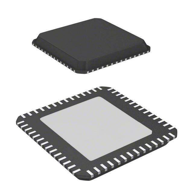
| 描述 | TVS DIODE 3.3VWM 12.3VC LLP753B |
| 产品分类 | |
| 品牌 | Vishay Semiconductor Diodes Division |
| 数据手册 | |
| 产品图片 | |
| 产品型号 | GSOT03-HT3-GS08 |
| rohs | 无铅 / 符合限制有害物质指令(RoHS)规范要求 |
| 产品系列 | - |
| 不同频率时的电容 | 420pF @ 1MHz |
| 产品目录绘图 |
|
| 产品目录页面 | |
| 供应商器件封装 | LLP75-3B |
| 其它名称 | 751-1402-6 |
| 功率-峰值脉冲 | 369W |
| 包装 | Digi-Reel® |
| 单向通道 | 1 |
| 双向通道 | - |
| 安装类型 | 表面贴装 |
| 封装/外壳 | 3-WDFN |
| 工作温度 | -40°C ~ 125°C (TJ) |
| 应用 | 通用 |
| 标准包装 | 1 |
| 电压-击穿(最小值) | 4V |
| 电压-反向关态(典型值) | 3.3V (最小) |
| 电压-箝位(最大值)@Ipp | 12.3V |
| 电流-峰值脉冲(10/1000µs) | 30A (8/20µs) |
| 电源线路保护 | 无 |
| 类型 | 齐纳 |


- 商务部:美国ITC正式对集成电路等产品启动337调查
- 曝三星4nm工艺存在良率问题 高通将骁龙8 Gen1或转产台积电
- 太阳诱电将投资9.5亿元在常州建新厂生产MLCC 预计2023年完工
- 英特尔发布欧洲新工厂建设计划 深化IDM 2.0 战略
- 台积电先进制程称霸业界 有大客户加持明年业绩稳了
- 达到5530亿美元!SIA预计今年全球半导体销售额将创下新高
- 英特尔拟将自动驾驶子公司Mobileye上市 估值或超500亿美元
- 三星加码芯片和SET,合并消费电子和移动部门,撤换高东真等 CEO
- 三星电子宣布重大人事变动 还合并消费电子和移动部门
- 海关总署:前11个月进口集成电路产品价值2.52万亿元 增长14.8%


PDF Datasheet 数据手册内容提取
GSOT03-HT3 to GSOT36-HT3 Vishay Semiconductors Single-Line ESD-Protection in LLP75 Features • Single-line ESD-protection device Circuit Diagram (cid:129) ESD-immunity acc. IEC 61000-4-2 3 ± 30 kV contact discharge e3 ± 30 kV air discharge (cid:129) Space saving LLP package (cid:129) Lead (Pb)-free component 1 2 (cid:129) Lead finish = "e3" = matte tin (Sn) 20514 20417 (cid:129) Non-magnetic 1 (cid:129) "Green" molding compound (cid:129) Component in accordance to RoHS 2002/95/EC and WEEE 2002/96/EC Marking (example only) XX Dot = Pin 1 marking XX = Date code YY YY = Type code (see table below) 21001 Ordering Information Taped units per reel Device name Ordering code Minimum order quantity (8 mm tape on 7" reel) GSOT03-HT3 GSOT03-HT3-GS08 3000 15000 GSOT04-HT3 GSOT04-HT3-GS08 3000 15000 GSOT05-HT3 GSOT05-HT3-GS08 3000 15000 GSOT08-HT3 GSOT08-HT3-GS08 3000 15000 GSOT12-HT3 GSOT12-HT3-GS08 3000 15000 GSOT15-HT3 GSOT15-HT3-GS08 3000 15000 GSOT24-HT3 GSOT24-HT3-GS08 3000 15000 GSOT36-HT3 GSOT36-HT3-GS08 3000 15000 Package Data Package Marking Molding compound Device name Weight Moisture sensitivity level Soldering conditions name code flammability rating GSOT03-HT3 LLP75-3B A3 5.1 mg UL 94 V-0 MSL level 1 (according J-STD-020) 260 °C/10 s at terminals GSOT04-HT3 LLP75-3B A4 5.1 mg UL 94 V-0 MSL level 1 (according J-STD-020) 260 °C/10 s at terminals GSOT05-HT3 LLP75-3B A5 5.1 mg UL 94 V-0 MSL level 1 (according J-STD-020) 260 °C/10 s at terminals GSOT08-HT3 LLP75-3B A6 5.1 mg UL 94 V-0 MSL level 1 (according J-STD-020) 260 °C/10 s at terminals GSOT12-HT3 LLP75-3B A7 5.1 mg UL 94 V-0 MSL level 1 (according J-STD-020) 260 °C/10 s at terminals GSOT15-HT3 LLP75-3B A8 5.1 mg UL 94 V-0 MSL level 1 (according J-STD-020) 260 °C/10 s at terminals GSOT24-HT3 LLP75-3B A9 5.1 mg UL 94 V-0 MSL level 1 (according J-STD-020) 260 °C/10 s at terminals GSOT36-HT3 LLP75-3B AA 5.1 mg UL 94 V-0 MSL level 1 (according J-STD-020) 260 °C/10 s at terminals Document Number 85822 For technical support, please contact: ESD-Protection@vishay.com www.vishay.com Rev. 1.8, 21-Apr-08 1
GSOT03-HT3 to GSOT36-HT3 Vishay Semiconductors Absolute Maximum Ratings GSOT03-HT3 Rating Test condition Symbol Value Unit Pin 3 to 1 Peak pulse current Acc. IEC 61000-4-5, t = 8/20 µs; single shot IPPM 30 A P Pin 3 to 1 Peak pulse power Acc. IEC 61000-4-5, t = 8/20 µs; single shot PPP 369 W P Contact discharge acc. IEC 61000-4-2; 10 pulses VESD ± 30 kV ESD immunity Air discharge acc. IEC 61000-4-2; 10 pulses VESD ± 30 kV Operating temperature Junction temperature TJ - 40 to + 125 °C Storage temperature TSTG - 55 to + 150 °C GSOT04-HT3 Rating Test condition Symbol Value Unit Pin 3 to 1 Peak pulse current Acc. IEC 61000-4-5, t = 8/20 µs; single shot IPPM 30 A P Pin 3 to 1 Peak pulse power Acc. IEC 61000-4-5, t = 8/20 µs; single shot PPP 429 W P Contact discharge acc. IEC 61000-4-2; 10 pulses VESD ± 30 kV ESD immunity Air discharge acc. IEC 61000-4-2; 10 pulses VESD ± 30 kV Operating temperature Junction temperature TJ - 40 to + 125 °C Storage temperature TSTG - 55 to + 150 °C GSOT05-HT3 Rating Test condition Symbol Value Unit Pin 3 to 1 Peak pulse current Acc. IEC 61000-4-5, t = 8/20 µs; single shot IPPM 30 A P Pin 3 to 1 Peak pulse power Acc. IEC 61000-4-5, t = 8/20 µs; single shot PPP 480 W P Contact discharge acc. IEC 61000-4-2; 10 pulses VESD ± 30 kV ESD immunity Air discharge acc. IEC 61000-4-2; 10 pulses VESD ± 30 kV Operating temperature Junction temperature TJ - 40 to + 125 °C Storage temperature TSTG - 55 to + 150 °C GSOT08-HT3 Rating Test condition Symbol Value Unit Pin 3 to 1 Peak pulse current Acc. IEC 61000-4-5, t = 8/20 µs; single shot IPPM 18 A P Pin 3 to 1 Peak pulse power Acc. IEC 61000-4-5, t = 8/20 µs; single shot PPP 345 W P Contact discharge acc. IEC 61000-4-2; 10 pulses VESD ± 30 kV ESD immunity Air discharge acc. IEC 61000-4-2; 10 pulses VESD ± 30 kV Operating temperature Junction temperature TJ - 40 to + 125 °C Storage temperature TSTG - 55 to + 150 °C www.vishay.com For technical support, please contact: ESD-Protection@vishay.com Document Number 85822 2 Rev. 1.8, 21-Apr-08
GSOT03-HT3 to GSOT36-HT3 Vishay Semiconductors GSOT12-HT3 Rating Test condition Symbol Value Unit Pin 3 to 1 Peak pulse current Acc. IEC 61000-4-5, t = 8/20 µs; single shot IPPM 12 A P Pin 3 to 1 Peak pulse power Acc. IEC 61000-4-5, t = 8/20 µs; single shot PPP 312 W P Contact discharge acc. IEC 61000-4-2; 10 pulses VESD ± 30 kV ESD immunity Air discharge acc. IEC 61000-4-2; 10 pulses VESD ± 30 kV Operating temperature Junction temperature TJ - 40 to + 125 °C Storage temperature TSTG - 55 to + 150 °C GSOT15-HT3 Rating Test condition Symbol Value Unit Pin 3 to 1 Peak pulse current Acc. IEC 61000-4-5, t = 8/20 µs; single shot IPPM 8 A P Pin 3 to 1 Peak pulse power Acc. IEC 61000-4-5, t = 8/20 µs; single shot PPP 230 W P Contact discharge acc. IEC 61000-4-2; 10 pulses VESD ± 30 kV ESD immunity Air discharge acc. IEC 61000-4-2; 10 pulses VESD ± 30 kV Operating temperature Junction temperature TJ - 40 to + 125 °C Storage temperature TSTG - 55 to + 150 °C GSOT24-HT3 Rating Test condition Symbol Value Unit Pin 3 to 1 Peak pulse current Acc. IEC 61000-4-5, t = 8/20 µs; single shot IPPM 5 A P Pin 3 to 1 Peak pulse power Acc. IEC 61000-4-5, t = 8/20 µs; single shot PPP 235 W P Contact discharge acc. IEC 61000-4-2; 10 pulses VESD ± 30 kV ESD immunity Air discharge acc. IEC 61000-4-2; 10 pulses VESD ± 30 kV Operating temperature Junction temperature TJ - 40 to + 125 °C Storage temperature TSTG - 55 to + 150 °C GSOT36-HT3 Rating Test condition Symbol Value Unit Pin 3 to 1 Peak pulse current Acc. IEC 61000-4-5, t = 8/20 µs; single shot IPPM 3.5 A P Pin 3 to 1 Peak pulse power Acc. IEC 61000-4-5, t = 8/20 µs; single shot PPP 248 W P Contact discharge acc. IEC 61000-4-2; 10 pulses VESD ± 30 kV ESD immunity Air discharge acc. IEC 61000-4-2; 10 pulses VESD ± 30 kV Operating temperature Junction temperature TJ - 40 to + 125 °C Storage temperature TSTG - 55 to + 150 °C Document Number 85822 For technical support, please contact: ESD-Protection@vishay.com www.vishay.com Rev. 1.8, 21-Apr-08 3
GSOT03-HT3 to GSOT36-HT3 Vishay Semiconductors BiAs-Mode (1-line Bidirectional Asymmetrical protection mode) With the GSOTxx-HT3 one signal- or data-lines (L1) can be protected against voltage transients. With pin 1 connected to ground and pin 3 connected to a signal- or data-line which has to be protected. As long as the voltage level on the data- or signal-line is between 0 V (ground level) and the specified Maximum Reverse Working Voltage (V ) the protection diode between pin 2 and pin 3 offer a high isolation to the ground line. RWM The protection device behaves like an open switch. As soon as any positive transient voltage signal exceeds the break through voltage level of the protection diode, the diode becomes conductive and shorts the transient current to ground. Now the protection device behaves like a closed switch. The Clamping Voltage (V ) is defined by the BReakthrough Voltage (V ) level C BR plus the voltage drop at the series impedance (resistance and inductance) of the protection device. Any negative transient signal will be clamped accordingly. The negative transient current is flowing in the forward direction of the protection diode. The low Forward Voltage (V ) clamps the negative transient close to F the ground level. Due to the different clamping levels in forward and reverse direction the GSOTxx-HT3 clamping behaviour is Bidirectional and Asymmetrical (BiAs). L1 3 1 2 20418 Electrical Characteristics Ratings at 25°C ambient temperature unless otherwise specified GSOT03-HT3 BiAs mode (between pin 3 to 1) Parameter Test conditions/remarks Symbol Min. Typ. Max. Unit Protection paths Number of lines which can be protected Nlines 1 lines Reverse stand off voltage at IR = 100 µA VRWM 3.3 V Reverse current at VR = 3.3 V IR 100 µA Reverse break down voltage at IR = 1 mA VBR 4 4.6 V at IPP = 1 A VC 5.7 7.5 V Reverse clamping voltage at IPP = IPPM = 30 A VC 10 12.3 V at IPP = 1 A VF 1 1.2 V Forward clamping voltage at IPP = IPPM = 30 A VF 4.5 V at VR = 0 V; f = 1 MHz CD 420 600 pF Capacitance at VR = 1.6 V; f = 1 MHz CD 260 pF www.vishay.com For technical support, please contact: ESD-Protection@vishay.com Document Number 85822 4 Rev. 1.8, 21-Apr-08
GSOT03-HT3 to GSOT36-HT3 Vishay Semiconductors GSOT04-HT3 BiAs mode (between pin 3 to 1) Parameter Test conditions/remarks Symbol Min. Typ. Max. Unit Protection paths Number of lines which can be protected Nlines 1 lines Reverse stand off voltage at IR = 20 µA VRWM 4 V Reverse current at VR = 4 V IR 20 µA Reverse break down voltage at IR = 1 mA VBR 5 6.1 V at IPP = 1 A VC 7.5 9 V Reverse clamping voltage at IPP = IPPM = 30 A VC 11.2 14.3 V at IPP = 1 A VF 1 1.2 V Forward clamping voltage at IPP = IPPM = 30 A VF 4.5 V at VR = 0 V; f = 1 MHz CD 310 450 pF Capacitance at VR = 2 V; f = 1 MHz CD 200 pF GSOT05-HT3 BiAs mode (between pin 3 to 1) Parameter Test conditions/remarks Symbol Min. Typ. Max. Unit Protection paths Number of lines which can be protected Nlines 1 lines Reverse stand off voltage at IR = 10 µA VRWM 5 V Reverse current at VR = 5 V IR 10 µA Reverse break down voltage at IR = 1 mA VBR 6 6.8 V at IPP = 1 A VC 7 8.7 V Reverse clamping voltage at IPP = IPPM = 30 A VC 12 16 V at IPP = 1 A VF 1 1.2 V Forward clamping voltage at IPP = IPPM = 30 A VF 4.5 V at VR = 0 V; f = 1 MHz CD 260 350 pF Capacitance at VR = 2.5 V; f = 1 MHz CD 150 pF GSOT08-HT3 BiAs mode (between pin 3 to 1) Parameter Test conditions/remarks Symbol Min. Typ. Max. Unit Protection paths Number of lines which can be protected Nlines 1 lines Reverse stand off voltage at IR = 5 µA VRWM 8 V Reverse current at VR = 8 V IR 5 µA Reverse break down voltage at IR = 1 mA VBR 9 10 V at IPP = 1 A VC 10.7 13 V Reverse clamping voltage at IPP = IPPM = 18 A VC 15.2 19.2 V at IPP = 1 A VF 1 1.2 V Forward clamping voltage at IPP = IPPM = 18 A VF 3 V at VR = 0 V; f = 1 MHz CD 160 250 pF Capacitance at VR = 4 V; f = 1 MHz CD 80 pF Document Number 85822 For technical support, please contact: ESD-Protection@vishay.com www.vishay.com Rev. 1.8, 21-Apr-08 5
GSOT03-HT3 to GSOT36-HT3 Vishay Semiconductors GSOT12-HT3 BiAs mode (between pin 3 to 1) Parameter Test conditions/remarks Symbol Min. Typ. Max. Unit Protection paths Number of lines which can be protected Nlines 1 lines Reverse stand off voltage at IR = 1 µA VRWM 12 V Reverse current at VR = 12 V IR 1 µA Reverse break down voltage at IR = 1 mA VBR 13.5 15 V at IPP = 1 A VC 15.4 18.7 V Reverse clamping voltage at IPP = IPPM = 12 A VC 21.2 26 V at IPP = 1 A VF 1 1.2 V Forward clamping voltage at IPP = IPPM = 12 A VF 2.2 V at VR = 0 V; f = 1 MHz CD 115 150 pF Capacitance at VR = 6 V; f = 1 MHz CD 50 pF GSOT15-HT3 BiAs mode (between pin 3 to 1) Parameter Test conditions/remarks Symbol Min. Typ. Max. Unit Protection paths Number of lines which can be protected Nlines 1 lines Reverse stand off voltage at IR = 1 µA VRWM 15 V Reverse current at VR = 15 V IR 1 µA Reverse break down voltage at IR = 1 mA VBR 16.5 18 V at IPP = 1 A VC 19.4 23.5 V Reverse clamping voltage at IPP = IPPM = 8 A VC 24.8 28.8 V at IPP = 1 A VF 1 1.2 V Forward clamping voltage at IPP = IPPM = 8 A VF 1.8 V at VR = 0 V; f = 1 MHz CD 90 120 pF Capacitance at VR = 7.5 V; f = 1 MHz CD 35 pF GSOT24-HT3 BiAs mode (between pin 3 to 1) Parameter Test conditions/remarks Symbol Min. Typ. Max. Unit Protection paths Number of lines which can be protected Nlines 1 lines Reverse stand off voltage at IR = 1 µA VRWM 24 V Reverse current at VR = 24 V IR 1 µA Reverse break down voltage at IR = 1 mA VBR 27 30 V at IPP = 1 A VC 34 41 V Reverse clamping voltage at IPP = IPPM = 5 A VC 41 47 V at IPP = 1 A VF 1 1.2 V Forward clamping voltage at IPP = IPPM = 5 A VF 1.4 V at VR = 0 V; f = 1 MHz CD 65 80 pF Capacitance at VR = 12 V; f = 1 MHz CD 20 pF www.vishay.com For technical support, please contact: ESD-Protection@vishay.com Document Number 85822 6 Rev. 1.8, 21-Apr-08
GSOT03-HT3 to GSOT36-HT3 Vishay Semiconductors GSOT36-HT3 BiAs mode (between pin 3 to 1) Parameter Test conditions/remarks Symbol Min. Typ. Max. Unit Protection paths Number of lines which can be protected Nlines 1 lines Reverse stand off voltage at IR = 1 µA VRWM 36 V Reverse current at VR = 36 V IR 1 µA Reverse break down voltage at IR = 1 mA VBR 39 43 V at IPP = 1 A VC 49 60 V Reverse clamping voltage at IPP = IPPM = 3.5 A VC 59 71 V at IPP = 1 A VF 1 1.2 V Forward clamping voltage at IPP = IPPM = 3.5 A VF 1.3 V at VR = 0 V; f = 1 MHz CD 52 65 pF Capacitance at VR = 18 V; f = 1 MHz CD 12 pF Package Dimensions in millimeters (inches): LLP75-3B 18057 Document Number 85822 For technical support, please contact: ESD-Protection@vishay.com www.vishay.com Rev. 1.8, 21-Apr-08 7
GSOT03-HT3 to GSOT36-HT3 Vishay Semiconductors Ozone Depleting Substances Policy Statement It is the policy of Vishay Semiconductor GmbH to 1. Meet all present and future national and international statutory requirements. 2. Regularly and continuously improve the performance of our products, processes, distribution and operating systems with respect to their impact on the health and safety of our employees and the public, as well as their impact on the environment. It is particular concern to control or eliminate releases of those substances into the atmosphere which are known as ozone depleting substances (ODSs). The Montreal Protocol (1987) and its London Amendments (1990) intend to severely restrict the use of ODSs and forbid their use within the next ten years. Various national and international initiatives are pressing for an earlier ban on these substances. Vishay Semiconductor GmbH has been able to use its policy of continuous improvements to eliminate the use of ODSs listed in the following documents. 1. Annex A, B and list of transitional substances of the Montreal Protocol and the London Amendments respectively. 2. Class I and II ozone depleting substances in the Clean Air Act Amendments of 1990 by the Environmental Protection Agency (EPA) in the USA. 3. Council Decision 88/540/EEC and 91/690/EEC Annex A, B and C (transitional substances) respectively. Vishay Semiconductor GmbH can certify that our semiconductors are not manufactured with ozone depleting substances and do not contain such substances. We reserve the right to make changes to improve technical design and may do so without further notice. Parameters can vary in different applications. All operating parameters must be validated for each customer application by the customer. Should the buyer use Vishay Semiconductors products for any unintended or unauthorized application, the buyer shall indemnify Vishay Semiconductors against all claims, costs, damages, and expenses, arising out of, directly or indirectly, any claim of personal damage, injury or death associated with such unintended or unauthorized use. Vishay Semiconductor GmbH, P.O.B. 3535, D-74025 Heilbronn, Germany www.vishay.com For technical support, please contact: ESD-Protection@vishay.com Document Number 85822 8 Rev. 1.8, 21-Apr-08
Legal Disclaimer Notice Vishay Disclaimer All product specifications and data are subject to change without notice. Vishay Intertechnology, Inc., its affiliates, agents, and employees, and all persons acting on its or their behalf (collectively, “Vishay”), disclaim any and all liability for any errors, inaccuracies or incompleteness contained herein or in any other disclosure relating to any product. Vishay disclaims any and all liability arising out of the use or application of any product described herein or of any information provided herein to the maximum extent permitted by law. The product specifications do not expand or otherwise modify Vishay’s terms and conditions of purchase, including but not limited to the warranty expressed therein, which apply to these products. No license, express or implied, by estoppel or otherwise, to any intellectual property rights is granted by this document or by any conduct of Vishay. The products shown herein are not designed for use in medical, life-saving, or life-sustaining applications unless otherwise expressly indicated. Customers using or selling Vishay products not expressly indicated for use in such applications do so entirely at their own risk and agree to fully indemnify Vishay for any damages arising or resulting from such use or sale. Please contact authorized Vishay personnel to obtain written terms and conditions regarding products designed for such applications. Product names and markings noted herein may be trademarks of their respective owners. Document Number: 91000 www.vishay.com Revision: 18-Jul-08 1