ICGOO在线商城 > 传感器,变送器 > 光学传感器 - 反射式 - 模拟输出 > GP2S60B
 Datasheet下载
- 型号: GP2S60B
- 制造商: Sharp Microelectronics
- 库位|库存: xxxx|xxxx
- 要求:
| 数量阶梯 | 香港交货 | 国内含税 |
| +xxxx | $xxxx | ¥xxxx |
查看当月历史价格
查看今年历史价格
GP2S60B产品简介:
ICGOO电子元器件商城为您提供GP2S60B由Sharp Microelectronics设计生产,在icgoo商城现货销售,并且可以通过原厂、代理商等渠道进行代购。 GP2S60B价格参考。Sharp MicroelectronicsGP2S60B封装/规格:光学传感器 - 反射式 - 模拟输出, Reflective Optical Sensor 0.028" (0.7mm) 4-SMD, No Lead。您可以下载GP2S60B参考资料、Datasheet数据手册功能说明书,资料中有GP2S60B 详细功能的应用电路图电压和使用方法及教程。
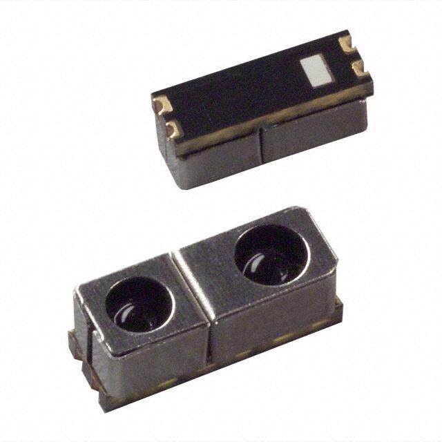
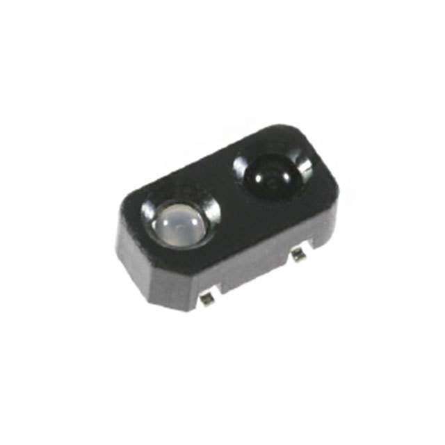
SHARP(由Socle Technology支持)生产的GP2S60B是一款反射式光学传感器,具备模拟输出功能。该传感器通过红外发射管和光电晶体管组合,检测物体与传感器之间的距离或表面反射率变化,输出连续的模拟电压信号,适用于需要精细距离或位置反馈的场景。

GP2S60B广泛应用于小型电子设备和工业控制系统中。常见用途包括:打印机、复印机等办公设备中用于纸张检测,判断是否有卡纸或纸尽情况;在自动售货机中检测商品是否掉落或出货完成;也可用于家用电器如扫地机器人中实现边缘或障碍物感应,辅助导航避障。此外,在工业自动化领域,该传感器可用于流水线上的物体定位、计数或位置校准,提高生产效率与精度。

由于其体积小巧、响应速度快、可靠性高,GP2S60B特别适合空间受限且对稳定性要求较高的应用环境。其模拟输出特性使其能提供更细腻的距离信息,相比数字输出传感器更适合需要连续监测的应用场合。总体而言,GP2S60B是一款性能稳定、应用灵活的反射式光电传感器,适用于多种需要非接触式检测的中低精度场景。
| 参数 | 数值 |
| 产品目录 | |
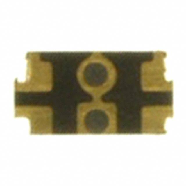
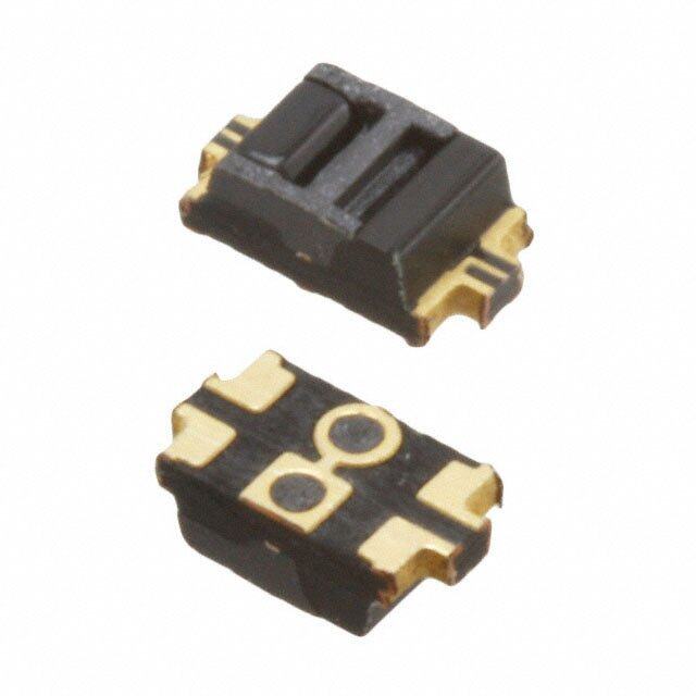
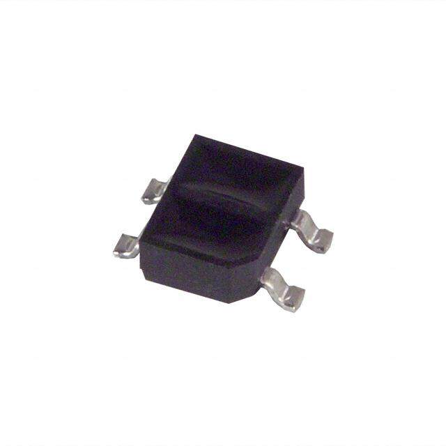
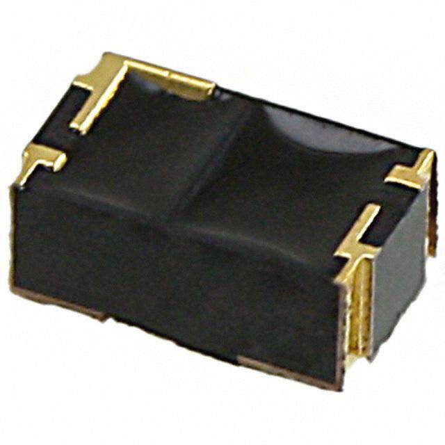
| 描述 | PHOTOINTERRUPTER TRANS OUT 4X3光学开关(反射型,光电晶体管输出) Photointerrupter 65~130uA |
| 产品分类 | |
| 品牌 | Sharp Microelectronics |
| 产品手册 | |
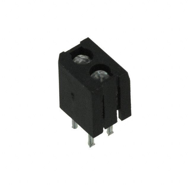
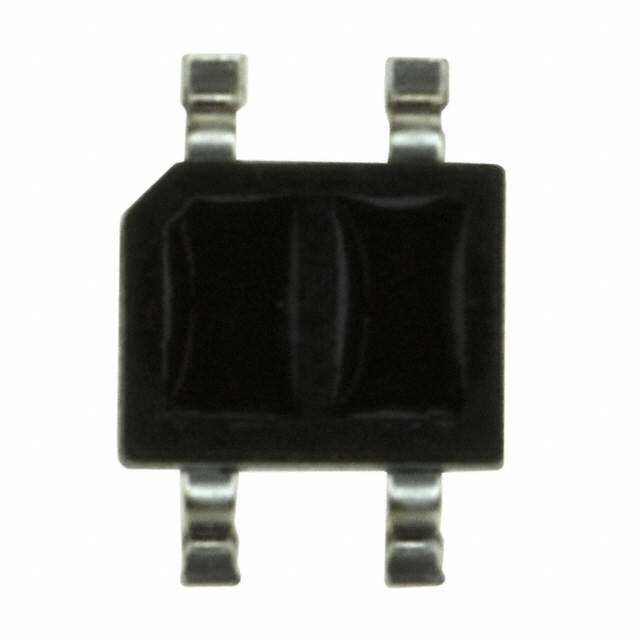
| 产品图片 |
|
| rohs | 符合RoHS无铅 / 符合限制有害物质指令(RoHS)规范要求 |
| 产品系列 | 光学开关(反射型,光电晶体管输出),Sharp Microelectronics GP2S60B- |
| 数据手册 | http://www.sharpsma.com/webfm_send/1267 |
| 产品型号 | GP2S60B |
| PCN设计/规格 | http://www.sharpsma.com/webfm_send/1525 |
| 上升时间 | 20 us |
| 下降时间 | 20 us |
| 产品目录页面 | |
| 产品种类 | 光学开关(反射型,光电晶体管输出) |
| 其它名称 | 425-2670-1 |
| 包装 | 剪切带 (CT) |
| 反向电压 | 6 V |
| 响应时间 | 20µs, 20µs |
| 商标 | Sharp Microelectronics |
| 安装类型 | 表面贴装 |
| 安装风格 | SMD/SMT |
| 封装 | Reel |
| 封装/外壳 | 4-SMD,无引线 |
| 工作温度 | -25°C ~ 85°C |
| 工厂包装数量 | 2000 |
| 感应方式 | Reflective |
| 感应方法 | 反射 |
| 感应距离 | 0.028"(0.7mm) |
| 最大工作温度 | + 85 C |
| 最大集电极电流 | 20 mA |
| 最小工作温度 | - 25 C |
| 标准包装 | 1 |
| 正向电压 | 1.2 V |
| 正向电流 | 20 mA |
| 波长 | 950 nm |
| 电压-集射极击穿(最大值) | 35V |
| 电流-DC正向(If) | 50mA |
| 电流-集电极(Ic)(最大值) | 20mA |
| 输出类型 | 光电晶体管 |
| 输出设备 | Phototransistor |
| 集电极—发射极最大电压VCEO | 35 V |


- 商务部:美国ITC正式对集成电路等产品启动337调查
- 曝三星4nm工艺存在良率问题 高通将骁龙8 Gen1或转产台积电
- 太阳诱电将投资9.5亿元在常州建新厂生产MLCC 预计2023年完工
- 英特尔发布欧洲新工厂建设计划 深化IDM 2.0 战略
- 台积电先进制程称霸业界 有大客户加持明年业绩稳了
- 达到5530亿美元!SIA预计今年全球半导体销售额将创下新高
- 英特尔拟将自动驾驶子公司Mobileye上市 估值或超500亿美元
- 三星加码芯片和SET,合并消费电子和移动部门,撤换高东真等 CEO
- 三星电子宣布重大人事变动 还合并消费电子和移动部门
- 海关总署:前11个月进口集成电路产品价值2.52万亿元 增长14.8%

PDF Datasheet 数据手册内容提取
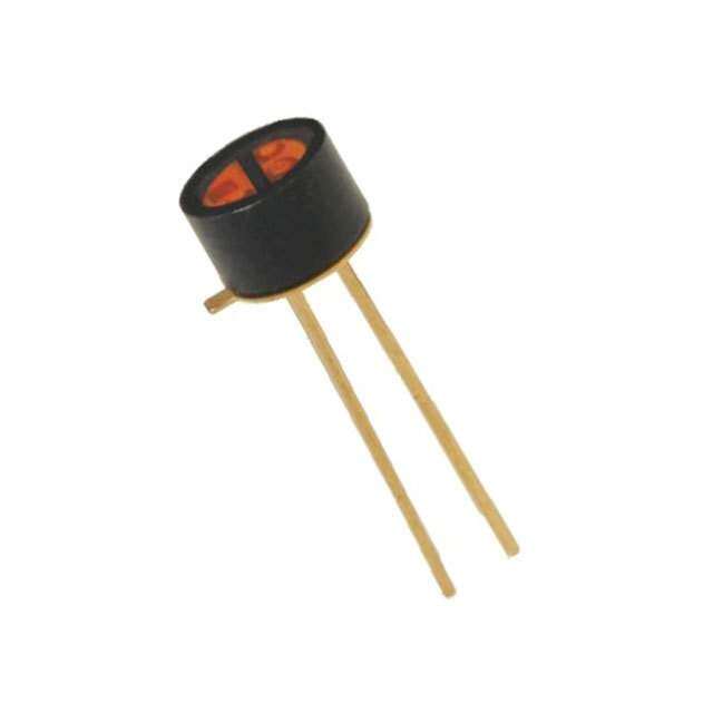
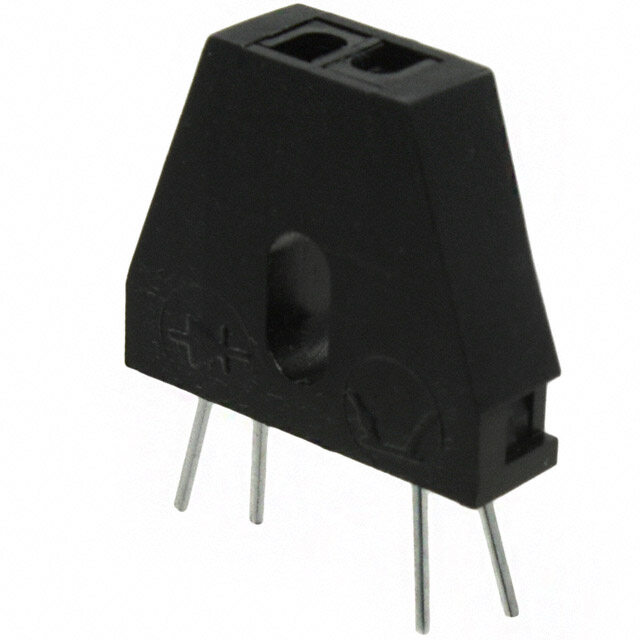
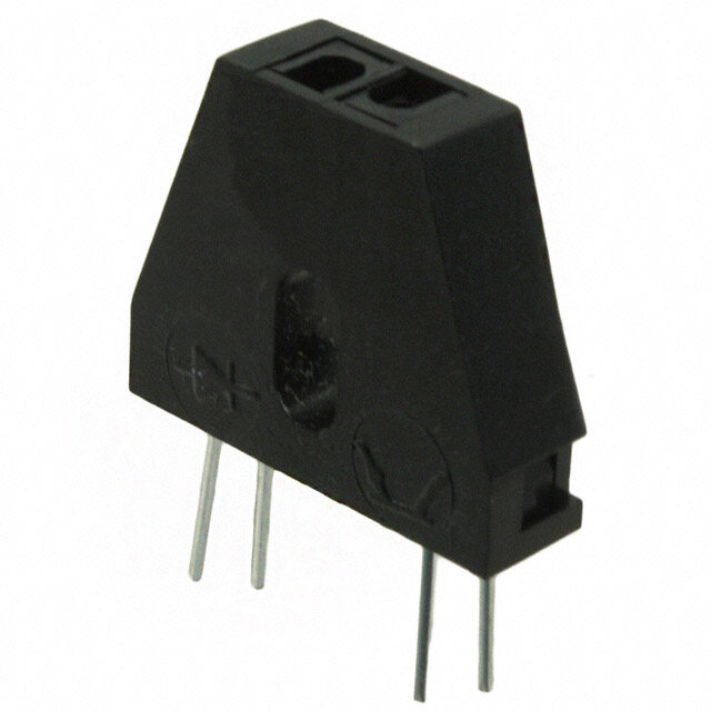
GP2S60 SMT, Detecting Distance : 0.5mm GP2S60 Phototransistor Output, Compact Reflective Photointerrupter ■ Description ■Agency approvals/Compliance GP2S60 is a compact-package, phototransistor output, 1. Compliant with RoHS directive reflective photointerrupter, with emitter and detector facing the same direction in a molding that provides noncontact sensing. ■Applications The compact package series is a result of unique technology, 1. Detection of object presence or motion. combing transfer and injection molding, that also blocks visible 2. Any application, which production is migrating to light to minimize false detection. 100% surface mount components. This photointerrupter can be ordered in different CTR ranks, Example : printer, optical storage and has a thin, leadless (T&R) package, suitable for reflow soldering. ■Features 1. Reflective with Phototransistor Output 2. Highlights : • Compact Size • Surface Mount Type (SMT), reflow soldering • Tape and Reel (T&R) 2 000 pcs per reel 3. Key Parameters : • Optimal Sensing Distance : 0.5mm • Package : 3.2×1.7×1.1mm • Visible light cut resin to prevent 4. RoHS directive compliant Notice The content of data sheet is subject to change without prior notice. In the absence of confirmation by device specification sheets, SHARP takes no responsibility for any defects that may occur in equipment using any SHARP devices shown in catalogs, data books, etc. Contact SHARP in order to obtain the latest device specification sheets before using any SHARP device. Sheet No.:D3-A02101EN-A 1
GP2S60 ■ Internal Connection Diagram Top view ① Collector ① ④ ② Emitter ③ Cathode ④ Anode ② ③ ■ Outline Dimensions (Unit : mm) Top view (0.7) Detector center 7 5) 1. 5 0. ( (0.7) 3) 5) 6 6 Emitter center 0. 0. ( ( 2.7 3.2 Opaque resin molding portion 4 0. 1 1. (1.8) 7) 0.5 ( ② ③ Plating area ① ④ Pattern for directional 7) 5 Distinction (NC) 0. ( • Unspecified tolerance : ±0.15mm. • Dimensions in parenthesis are shown for reference. • Dimensions on the outline drawing is the maximum value excluding burr. • The dimensions shown do not include burr. • Burr's dimension : 0.15mm MAX. Product mass : approx. 0.01g Plating material : Au Sheet No.: D3-A02101EN-A 2
GP2S60 ■Absolute Maximum Ratings (Ta=25˚C) Parameter Symbol Rating Unit Forward current I 50 mA F Input Reverse voltage V 6 V R Power dissipation P 75 mW D Collector-emitter voltage V 35 V CEO Emitter-collector voltage V 6 V Output ECO Collector current I 20 mA C Collector power dissipation P 75 mW C Total power dissipation P 100 mW tot Operating temperature Topr −25 to +85 ˚C Storage temperature Tstg −40 to +100 ˚C ∗1Soldering temperature T 260 ˚C sol ∗1 For 5s or less ■Electro-optical Characteristics (Ta=25˚C) Parameter Symbol Condition MIN. TYP. MAX. Unit Input Forward voltage VF IF=20mA − 1.2 1.4 V Reverse current IR VR=6V − − 10 μA Output Collector dark current ICEO VCE=20V − 1 100 nA Transfer ∗2 Collector Current IC IF=4mA, VCE=2V 40 85 130 μA charac- ∗3 Leak current ILEAK IF=4mA, VCE=2V − − 500 nA teristics Response time Rise time tr VCE=2V, IC=100μA, − 20 100 μs Fall time tf RL=1kΩ, d=1mm − 20 100 ∗2 The condition and arrangement of the refl ective object are shown below. The rank splitting of collector current (IC) shall be executed according to the table below. Rank Collector current, IC [μA] (IF=4mA, VCE=2V) A 40 to 80 B 65 to 130 ∗3 Without refl ective object. ●Test Condition and Arrangement for Collector Current Aluminum evaporation d=1mm glass plate Sheet No.:D3-A02101EN-A 3
GP2S60 ■Model Line-up Model No. Rank IC(μA) Conditions GP2S60 A or B 40 to 130 IF=4mA GP2S60A A 40 to 80 VCE=2V GP2S60B B 65 to 130 Ta=25˚C Please contact a local SHARP sales representative to see the actial status of the produiction. Sheet No.:D3-A02101EN-A 4
GP2S60 Fig.1 Forward Current vs. Ambient Fig.2 Power Dissipation vs. Temperature Ambient Temperature 60 120 W) m Ptot 50 (Ptot 100 A) , C (mF 40 P, PD 8705 PD,PC nt I on ward curre 2300 er dissipati 4600 For Pow 10 20 15 0 0 (cid:13)25 0 25 50 75 85 100 −25 0 25 50 75 85 100 Ambient temperature Ta (˚C) Ambient temperature Ta (˚C) Fig.3 Forward Current vs. Forward Fig.4 Collector Current vs. Voltage Forward Current 700 VCE=2V Ta=75˚C Ta=25C 50˚C 600 25˚C A) 100 0˚C A) 500 m μ d current I (F −25˚C or current I (C 340000 ar 10 ct w e For Coll 200 100 1 0 0 0.5 1 1.5 2 2.5 3 0 5 10 15 20 Forward voltage VF (V) Forward current IF (mA) Fig.5 Collector Current vs. Fig.6 Relative Collector Current vs. Collector-Emitter Voltage Ambient Temperature 600 120 Ta=25˚C IF=15mA IVFC=E4=m2AV 500 100 %) Collector current I (A)μC 234000000 107mmAA elative collector current ( 468000 4mA R 100 20 2mA 0 0 0 2 4 6 8 10 −25 0 25 50 75 Collector-emitter voltage VCE (V) Ambient temperature Ta (˚C) Sheet No.:D3-A02101EN-A 5
GP2S60 Fig.7 Collector Dark Current vs. Fig.8 Response Time vs. Load Ambient Temperature Resistance 10−6 1 000 VCE=20V IVCC=E1=020VμA Ta=25˚C (A)O 10−7 tr ark current ICE 10−8 onse time (s)μ 100 tf d p ctor Res 10 td olle 10−9 C ts 10−10 1 0 25 50 75 100 0.1 1 10 100 1 000 Ambient temperature Ta (˚C) Load resistance RL (kΩ) Fig.9 Test Circuit for Response Time Fig.10 Relative Collector Current vs. Distance 100 Al evaporation glass RPleaftleector VCC 90 IVFC=E4=m2AV L RD RL Input %) 80 Ta=25˚C Input OutputOutput ent ( 70 10% urr 60 c or 90% ct 50 ttdr ttsf e colle 40 v ati 30 el R 20 10 0 0.5 1 1.5 2 2.5 3 3.5 4 4.5 5 Distance between sensor and Aluminum evaporation glass L (mm) Fig.11 Spectral Sensitivity Fig.12 Detecting Position Characteristics (1) 100 100 OMS test card Ta=25˚C d 1mm Sensor 80 80 − 0 + %) vity (%) 60 current ( 60 VIdF=C=E14=mm2mAV nsiti ctor e e ve s 40 coll 40 ati ve Rel ati el R 20 20 0 600 700 800 900 1 000 1 100 1 200 −3 −2 −1 0 1 2 3 4 5 6 Wavelength λ (nm) OMS card moving distance (mm) Sheet No.:D3-A02101EN-A 6
GP2S60 Fig.13 Detecting Position Characteristics (2) 100 OMS test card d 1mm Sensor 80 − 0 + %) urrent ( 60 VIdF=C=E14=mm2mAV c or ct e coll 40 e v ati el R 20 −3 −2 −1 0 1 2 3 4 5 6 OMS card moving distance (mm) Remarks : Please be aware that all data in the graph are just for reference and not for guarantee. Sheet No.:D3-A02101EN-A 7
GP2S60 ■Design Considerations ●Design guide 1) Regarding to prevention of malfunction To prevent photointerrupter from faulty operation caused by external light, do not set the detecting face to the external light. 2) Distance characteristic The distance between the photointerrupter and the object to be detected shall be determined the distance by referencing Fig.10 "Relative collector current vs. distance". 3) For wiring on a mounting PCB To avoid possibility for short, please do not apply pattern wiring on the back side of the device. 4) Regarding to mounting this product There is a possibility that the opaque molded resin portion may have a crack by force at mounting etc. Please use this product after well confi rmation of conditions in your production line. This product is not designed against irradiation and incorporates non-coherent IRED. ●Degradation In the case of long term operation, please take the general IRED degradation (50% degradation over 5 years) into the design consideration. ●Parts This product is assembled using the below parts. • Light detector (qty. : 1) Maximum Sensitivity Sensitivity Category Material Response time (μs) wavelength (nm) wavelength (nm) Phototransister Silicon (Si) 930 700 to 1 200 20 • Light emitter (qty. : 1) Maximum light emitting Category Material I/O Frequency (MHz) wavelength (nm) Infrared emitting diode Gallium arsenide (GaAs) 950 0.3 (non-coherent) • Material Case PCB Lead frame plating Epoxy resin Glass epoxy resin Au plating Black polyphenylene sulfi de Sheet No.:D3-A02101EN-A 8
GP2S60 ● Recommended pattern (Unit : mm) measure tolerance : ±0.1 area : Please do not apply the pattern wiring to avoid the possibility of short circuit. Regarding amount of solder, if there is solder leakage in terminal wiring pattern between PCB and housing main body, the reliability will be deteriorated. Please check the proper amount of solder in advance not to have solder leakage into terminal wiring pattern between PCB and housing main body. Sheet No.: D3-A02101EN-A 9
GP2S60 ■Manufacturing Guidelines ●Storage and management after open Storage condition Storage temp.: 5 to 30˚C, Storage humidity : 70%RH or less at regular packaging. Treatment after opening the moisture-proof package After opening, you should mount the products while keeping them on the condition of 5 to 25˚C and 60%RH or less in humidity within 2 days. After opening the bag once even if the prolonged storage is necessary, you should mount the products within two weeks. And when you store the rest of products you should put into a DRY BOX. Otherwise after the rest of products and silicagel are sealed up again, you should keep them under the condition of 5 to 30˚C and 70%RH or less in humidity. Baking before mounting When the above-mentioned storage method could not be executed, please process the baking treatment before mounting the products. However the baking treatment is permitted within one time. Recommended condition : 125˚C, 16 to 24 hours ∗Do not process the baking treatment with the product wrapped. When the baking treatment processing, you should move the products to a metallic tray or fi x temporarily the products to substrate. Sheet No.:D3-A02101EN-A 10
GP2S60 ●Soldering Method Refl ow Soldering: Refl ow soldering should follow the temperature profi le shown below. Soldering should not exceed the curve of temperature profi le and time. Please solder within one time. MAX 240˚C 1 to 4˚C/s 200˚C MAX 165˚C 1 to 4˚C/s 1 to 4˚C/s 25˚C MAX10s MAX60s MAX120s MAX90s Other notice Please take care not to let any external force exert on lead pins. Please test the soldering method in actual condition and make sure the soldering works fine, since the impact on the junction between the device and PCB varies depending on the cooling and soldering conditions. ●Cleaning instructions Solvent cleaning : Solvent temperature should be 45˚C or below. Immersion time should be 3 minutes or less. Ultrasonic cleaning : Do not execute ultrasonic cleaning. Recommended solvent materials : Ethyl alcohol, Methyl alcohol and Isopropyl alcohol. Sheet No.:D3-A02101EN-A 11
GP2S60 ● Presence of ODC This product shall not contain the following materials. And they are not used in the production process for this product. Regulation substances : CFCs, Halon, Carbon tetrachloride, 1.1.1-Trichloroethane (Methylchloroform) Specific brominated flame retardants such as the PBBOs and PBBs are not used in this product at all. This product shall not contain the following materials banned in the RoHS Directive (2002/95/EC). •Lead, Mercury, Cadmium, Hexavalent chromium, Polybrominated biphenyls (PBB), Polybrominated diphenyl ethers (PBDE). Content of six substances specified in Management Methods for Control of Pollution Caused by Electronic Information Products Regulation (Chinese : 电子信息产品污染控制管理办法). Toxic and hazardous substances Hexavalent Polybrominated Polybrominated Category Lead Mercury Cadmium chromium biphenyls diphenyl ethers (Pb) (Hg) (Cd) (Cr6+) (PBB) (PBDE) Photointerrupter ✔ ✔ ✔ ✔ ✔ ✔ ✔ : indicates that the content of the toxic and hazardous substance in all the homogeneous materials of the part is below the concentration limit requirement as described in SJ/T 11363-2006 standard. Sheet No.: D3-A02101EN-A 12
GP2S60 ■ Package specification ● Tape and Reel package Package materials Carrier tape : PS (with anti-static material) Reel : PS Package method 2 000 pcs of products shall be packaged in a reel. One reed is endased in aluminum laminated bag. After sealing up the bag, it encased in one case (5 bags/case). Carrier tape structure and Dimensions Dimensions List (Unit:mm) A B C D E F 8±0.3 3.5±0.05 1.75±0.1 4±0.1 2±0.1 4±0.1 G H I J K L Φ1.55±0.05 3.6±0.1 0.3±0.05 1.25±0.1 2.2±0.1 Φ1.1±0.1 Reel structure and Dimensions Dimensions List (Unit:mm) a b c d 180±2.0 9±1.0 60+0.5 Φ13±0.2 -0 e f g Φ21±0.8 11.4±1.0 2+0.3 -0 Sheet No.: D3-A02101EN-A 13
GP2S60 Direction of product insertion Pull-out direction [Packing : 2 000pcs/reel] Storage method Storage conditions should follow the condition shown below. Storage temperature : 5 to 30˚C Storage hunidity : 70%RH or less Sheet No.:D3-A02101EN-A 14
GP2S60 ■ Important Notices · The circuit application examples in this publication are · Telecommunication equipment (Terminal) provided to explain representative applications of · Measuring equipment SHARP devices and are not intended to guarantee any · Tooling machines · Computers circuit design or license any intellectual property rights. If the use of the product in the above application areas is SHARP takes no responsibility for any problems related for equipment listed in paragraphs (2) or (3), please be to any intellectual property right of a third party resulting sure to observe the precautions given in those respective from the use of SHARP's devices. paragraphs. · Contact SHARP in order to obtain the latest device (2) Appropriate measures, such as fail-safe design and specification sheets before using any SHARP device. redundant design considering the safety design of the SHARP reserves the right to make changes in the overall system and equipment, should be taken to ensure specifications, characteristics, data, materials, structure, reliability and safety when this product is used for and other contents described herein at any time without equipment which demands high reliability and safety in notice in order to improve design or reliability. function and precision, such as ; Manufacturing locations are also subject to change · Transportation control and safety equipment (aircraft, without notice. train, automobile etc.) · Traffic signals · Gas leakage sensor breakers · These specification sheets include materials protected · Rescue and security equipment under copyright of Sharp Corporation ("Sharp"). · Other safety equipment Please do not reproduce or cause anyone to reproduce them without Sharp's consent. (3) Please do not use this product for equipment which require extremely high reliability and safety in function and · When using this product, please observe the absolute precision, such as ; maximum ratings and the instructions for use outlined in · Space equipment these specification sheets, as well as the precautions · Telecommunication equipment (for trunk lines) mentioned below. Sharp assumes no responsibility for · Nuclear power control equipment · Medical equipment any damage resulting from use of the product which does · Power generation and power transmission control not comply with the absolute maximum ratings and the system (Key system) instructions included in these specification sheets, and the precautions mentioned below. (4) Please contact and consult with a Sharp sales representative if there are any questions regarding · Please do verify the validity of this part after assembling interpretation of the above four paragraphs. it in customer’s products, when customer wants to make catalogue and instruction manual based on the · Please contact and consult with a Sharp sales specification sheet of this part. representative for any questions about this product. (Precautions) · If the SHARP devices listed in this publication fall within (1) This product is designed for use in the following the scope of strategic products described in the Foreign application areas ; Exchange and Foreign Trade Law of Japan, it is · OA equipment · Audio visual equipment necessary to obtain approval to export such SHARP · Home appliances devices. Sheet No.: D3-A02101EN-A 15