ICGOO在线商城 > 传感器,变送器 > 光学传感器 - 光电检测器 - 遥控接收器 > GP1UX311QS
 Datasheet下载
- 型号: GP1UX311QS
- 制造商: Sharp Microelectronics
- 库位|库存: xxxx|xxxx
- 要求:
| 数量阶梯 | 香港交货 | 国内含税 |
| +xxxx | $xxxx | ¥xxxx |
查看当月历史价格
查看今年历史价格
GP1UX311QS产品简介:
ICGOO电子元器件商城为您提供GP1UX311QS由Sharp Microelectronics设计生产,在icgoo商城现货销售,并且可以通过原厂、代理商等渠道进行代购。 GP1UX311QS价格参考。Sharp MicroelectronicsGP1UX311QS封装/规格:光学传感器 - 光电检测器 - 遥控接收器, Remote Receiver Sensor, 38.0kHz 8m Through Hole。您可以下载GP1UX311QS参考资料、Datasheet数据手册功能说明书,资料中有GP1UX311QS 详细功能的应用电路图电压和使用方法及教程。
Sharp Microelectronics的GP1UX311QS是一款一体化红外线接收器,常用于红外遥控信号的接收与处理。该器件集成了红外探测器、前置放大器和信号处理电路,能够接收并解调标准红外遥控器发射的38kHz调制信号。

GP1UX311QS广泛应用于以下场景:

1. 家用电器遥控接收:如电视、空调、音响、机顶盒等设备的红外遥控接收模块,实现用户远程控制功能。

2. 工业控制设备:用于工业自动化设备中的非接触式遥控或状态监测系统,提升操作便捷性与安全性。

3. 智能家居系统:作为智能中控设备的红外接收单元,实现对多种红外控制设备的集中管理与智能联动。

4. 教育及科研设备:用于实验开发板或教学设备中,帮助学生理解红外通信原理与应用。

5. 电子产品开发:作为模块化设计的一部分,用于快速开发具备红外接收功能的电子产品。

该器件具有高灵敏度、抗干扰能力强、安装方便等优点,是红外遥控系统中常用的接收元件。通常与微控制器配合使用,实现对遥控信号的识别与控制操作。
| 参数 | 数值 |
| B.P.F.中心频率 | 38.0kHz |
| 产品目录 | |
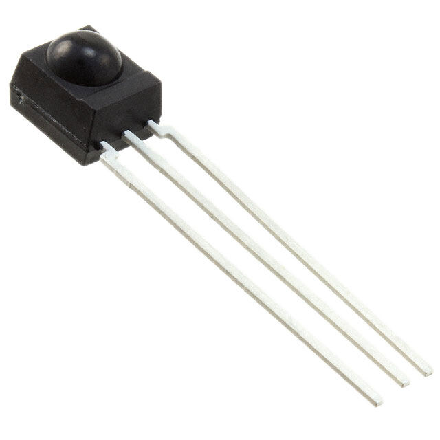
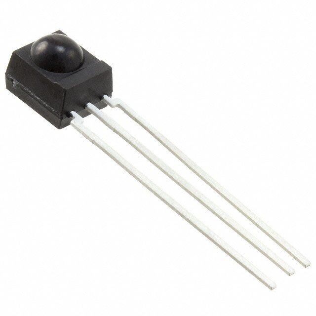
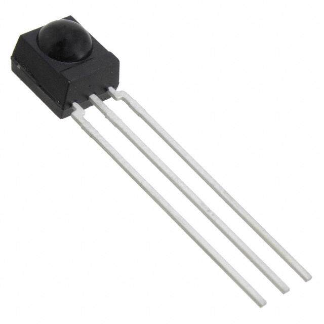
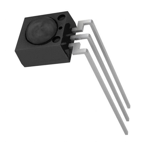
| 描述 | RECEIVER IR REM CTRL 3V 38KHZ红外接收机 Remote Cont Rec 3V 38 kHz |
| 产品分类 | |
| 品牌 | Sharp Microelectronics |
| 产品手册 | |
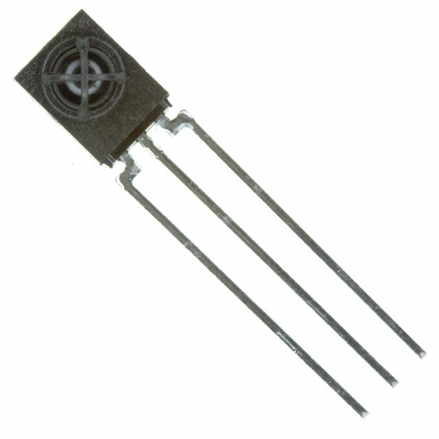
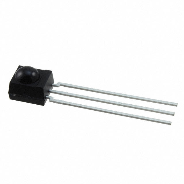
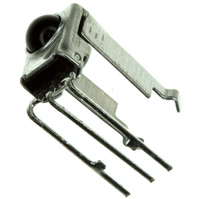
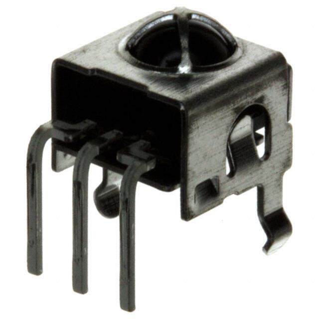
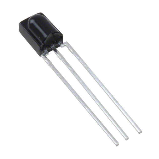
| 产品图片 |
|
| rohs | 符合RoHS无铅 / 符合限制有害物质指令(RoHS)规范要求 |
| 产品系列 | 红外接收机,Sharp Microelectronics GP1UX311QS- |
| 数据手册 | |
| 产品型号 | GP1UX311QS |
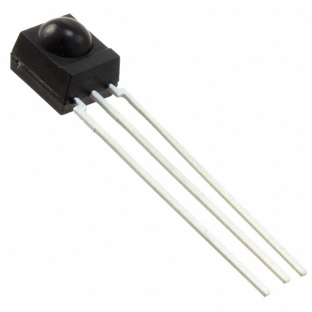
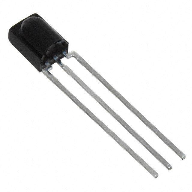
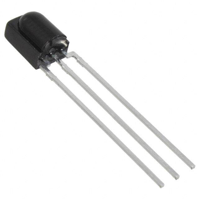
| 产品目录绘图 |
|
| 产品目录页面 | |
| 产品种类 | 红外接收机 |
| 传输距离 | 8 m |
| 低电平脉冲宽度 | 1000 us |
| 其它名称 | 425-2528 |
| 商标 | Sharp Microelectronics |
| 安装类型 | 通孔 |
| 安装风格 | Through Hole |
| 封装/箱体 | SIDE VIEW |
| 工作电源电压 | 2.7 V to 5.5 V |
| 工厂包装数量 | 500 |
| 感应距离 | 8m |
| 最大工作温度 | + 70 C |
| 最小工作温度 | - 10 C |
| 最小高电平输出电压 | 2.2 V |
| 朝向 | 侧视图 |
| 标准包装 | 500 |
| 电压-电源 | 2.7 V ~ 5.5 V |
| 电流-电源 | 400µA |
| 电源电流 | 0.27 mA |
| 载频 | 38 kHz |
| 高电平脉冲宽度 | 1200 us |


- 商务部:美国ITC正式对集成电路等产品启动337调查
- 曝三星4nm工艺存在良率问题 高通将骁龙8 Gen1或转产台积电
- 太阳诱电将投资9.5亿元在常州建新厂生产MLCC 预计2023年完工
- 英特尔发布欧洲新工厂建设计划 深化IDM 2.0 战略
- 台积电先进制程称霸业界 有大客户加持明年业绩稳了
- 达到5530亿美元!SIA预计今年全球半导体销售额将创下新高
- 英特尔拟将自动驾驶子公司Mobileye上市 估值或超500亿美元
- 三星加码芯片和SET,合并消费电子和移动部门,撤换高东真等 CEO
- 三星电子宣布重大人事变动 还合并消费电子和移动部门
- 海关总署:前11个月进口集成电路产品价值2.52万亿元 增长14.8%
PDF Datasheet 数据手册内容提取
GP1UX31QS Series GP1UX31QS Series Holder-less Type IR Detecting Unit for Remote Control Features Outline Dimensions (Unit : mm) 1.Holder-less shield case type. 2.Compact type. 3.Strengthened resistance to electromagnetic Conductive resin(GND) induction noise by double mold method. 5.5 2.1 3.2 4.Operarting voltage 3V type. 8 2. (cid:2) A(cid:2) pplications 7.5 6.9 6.0 8.8 4.1 1.AV equipments 2. Home appliances 1.6 8 3. Toys using IR sensor 2 1.2 0.4 Absolute Maximum Ratings 0.5 Vcc (cid:2) (Ta(cid:6)=25(cid:9) *1 2.54 GND Parameter Symbol Rating Unit Vout Supply voltage VCC 0 to (cid:5)+6.0 V *1 2.54 *1Operating temperature Topr -(cid:2)10 to +(cid:5)70 (cid:9) Storage temperature Tstg -(cid:2)20 to +(cid:5)70 (cid:9) Example of mounting drawing *2Soldering temperature T 265 (cid:9) from solder side (Reference) sol *1 No dew condensation is allowed Top of lenz *2 For 6s (At mounting on PCB with thickness of 1.6mm) 1. *1 : Indicates root dimensions of connector. 2. Unspecified tolerance:0.3 Recommended Operating Conditions (cid:2) Parameter Symbol Operating conditions Unit Supply voltage V 2.7 to 5.5 V CC NoticeThe content of data sheet is subject to change without prior notice. In the absence of confirmation by device specification sheets, SHARP takes no responsibility for any defects that may occur in equipment using any SHARP devices shown in catalogs, data books, etc. Contact SHARP in order to obtain the latest device specification sheets before using any SHARP device. Sheet No.: OP06013 1
GP1UX31QS Series Model Line-up (cid:2) Diversified models with a different B.P.F. frequency are also available. B.P.F. center frequency Model No. Unit 40 GP1UX31QS 36 GP1UX310QS kHz 38 GP1UX311QS 36.7 GP1UX312QS Internal Block Diagram RL VOUT Limiter B.P.F. Demodulator IntegratorComparator VCC GND Electro-optical Characteristics (cid:2) (Ta=25, V CC=3V) Parameter Symbol Conditions MIN. TYP. MAX. Unit Dissipation current ICC No input light (cid:2) 0.27 0.4 mA High level output voltage VOH *3 VCC -(cid:2)0.5 (cid:2) (cid:2) V Low level output voltage VOL *3 IOL(cid:6)=1.6mA (cid:2) (cid:2) 0.45 V High level pulse width T1 *3 600 (cid:2) 1200 s(cid:7) Low level pulse width T2 *3 400 (cid:2) 1000 s(cid:7) B.P.F. center frequency f (cid:2) (cid:2) *4 (cid:2) kHz 0 Output pull-up resistance RL (cid:2) 70 100 130 k(cid:8) *3The burst wave as shown in the following figure shall be transmitted by the transmitter shown in Fig. 1 The carrier frequency of the transmitter, however, shall be same as *4, and measurement shall be from just after starting the transmission until 50 pulse *4The B.P.F. center frequency f0 varies with model, as show(cid:2)n(cid:1) in Model Line-up Burst wave s 1000s f0=(*4) Duty 50% Output signal Sheet No.: OP06013 2
GP1UX31QS Series Performance Using the transmitter shown in Fig. 1, the output signal of the light detecting unit is good enough to meet the following items in the standard optical system in Fig. 2. 1. Linear reception distance characteristics When L=0.2 to 8.0m, *5EV 10 lx and in Fig.2, the output signal shall meet the electrical characteristics in the attached list. 2.Sensitivity angle reception distance characteristics When L=0.2 to 6.0m, *5EV 10 lx and 30in Fig.2, the output signal shall meet the electrical characteristics in the attached list. 3.Anti outer peripheral light reception distance characteristics When L=0.2 to 4.0m, *6EV 300 lx and in Fig.2, the output signal shall meet the electrical characteristics in the attached list. *5 It refers to detector face illuminance *6 Outer peripheral light source: CIE standard light source A shall be used and placed at 45from perpendicular axis at the detector face center Fig.1 Transmitter 20cm 10k(cid:8) (cid:5)5V PI 9 4 D 0 P 1 Transmitter (GL521 used) f0(cid:6)(*4) Duty 50% 0k(cid:8) VOUT 1 Oscilloscope In the above figure, the transmitter should be set so that the output VOUT (P-P) can be 40mV. However, the PD49PI to be used here should be of the short-circuit current ISC=2.6A at E V =100 lx. (E is an illuminance by CIE standard light source A (tungsten lamp).) V Fig.2 Standard Optical System Light detector face illuminance:EV VOUT Reception distance:L Transmitter ( indicates horizontal and vertical directions.) Sheet No.: OP06013 3
GP1UX31QS Series Precautions for Operation 1. When this infrared remote control detecting unit shall be adopted for wireless remote control, please use the following signal format . (NEC code,RC-6code etc.) Total duty ratio D t (Emitting time t N / Transmitting time for 1 block T) : 40% or less. ON signal time and OFF signal time Supply Voltage Vcc 2.7 3.0V 3.0 to 5.5V ON signal time per 1bit tON 200 s or more OFF signal time per 1bit tOFF 400 s or more 300 s or more Transmitting time for 1 block:T TON t1 t2 t3 tn (cid:12) (cid:6) In case the signal format of total duty and/or ON/OFF signal time dosen`t meet the conditions noted above, there is a case that reception distance much reduces or output dose not appear. 2. Use the light emitting unit (remote control transmitter), in consideration of performance, characteristics, operating conditions of light emitting device and the characteristics of the light detecting unit. 3. Pay attention to a malfunction of the light detecting unit when the surface is stained with dust and refuse. Care must be taken not to touch the light detector surface. If it should be dirty, wipe off such dust and refuse with soft cloth so as to prevent scratch. In case some solvents are required, use methyl alcohol, ethyl alcohol or isopropyl alcohol only. Also, protect the light detecting unit against flux and others, since their deposition on the unit inside causes reduction of the function, fading of markings such as the part number. 4. Unnecessary force shoud not be applied to terminal. 5. Do not push the light detector surface (photodiode) from outside. 6. To avoid the electrostatic breakdown of IC, handle the unit under the condition of grounding with human body, soldering iron, etc. 7. Since conductive thermo plasticity is used in 2nd mold regin,please be careful not to come in contact with PCB land pattern. 8. External Circuit Examples (Mount the outer parts as near the unit as possible). GND GND CO(cid:5) R1 VCC Ve (Circuit parameters) VOUT VO R1=(cid:6)475(cid:8)%(cid:4) C1=(cid:6)47F(cid:7) In setting R1 and C1, use suitable values after considering under the real condition The circuit constant is a example. It is difference from mounting equipment. Please select it by your mounting equipment. This device has a transistor as protection element between VCC and GND to improve anti-static electricity proof. Please be carefully not to apply exceeding the absolute maximum ratings of applying voltage and continuous high voltage spike noise because there is cases that transistor will be short by secondary breakdown generally. In order to do difficultly, Please add CR filter(47(1/10W), 10F or more)such as external circuit example above near V CC. Sheet No.: OP06013 4
GP1UX31QS Series 9. There is a possibility that noise on output may be caused by environmental condition (Disturbing light noise, Electromagnetic noise, Power supply line noise, etc.) even if there is no input transmission signal. 10. Please shall confirm operation or your actual machine. Because the output pulse width of this product is fluctuated by environmental conditions such as signal format, temperature, distance from transmitter, and so on. 11. In case that this product is kept in high humidity condition, it may be hard to solder, please be careful enough about storage method. Depend on the flux you select, there are different solderabilities, so please select a suitable flux and use it. 12. This product dose`t correspond to soldering by reflow. 13. Please make sure in case pf hand soldering that yue the solder iron with less than 45W power and solder iron point(edge) temperature is less than 320 within 3 seconds,and also don't add any force to lead frame directly.And please make sure never to touch 2nd mold resin by a solding. 14. When using this device,please be careful not to cause dew drop. Be aware that the dew drop rusts lead pins portion and others, may affect the electric characteristics. 15. The lead flame may be deformed since the device is packed in vinyl bag. Sheet No.: OP06013 5