ICGOO在线商城 > 传感器,变送器 > 光学传感器 - 光电检测器 - 遥控接收器 > TSOP32236

 Datasheet下载
- 型号: TSOP32236
- 制造商: Vishay
- 库位|库存: xxxx|xxxx
- 要求:
| 数量阶梯 | 香港交货 | 国内含税 |
| +xxxx | $xxxx | ¥xxxx |
查看当月历史价格
查看今年历史价格
TSOP32236产品简介:
ICGOO电子元器件商城为您提供TSOP32236由Vishay设计生产,在icgoo商城现货销售,并且可以通过原厂、代理商等渠道进行代购。 TSOP32236价格参考¥2.47-¥2.47。VishayTSOP32236封装/规格:光学传感器 - 光电检测器 - 遥控接收器, Remote Receiver Sensor, 36.0kHz 45m Through Hole。您可以下载TSOP32236参考资料、Datasheet数据手册功能说明书,资料中有TSOP32236 详细功能的应用电路图电压和使用方法及教程。
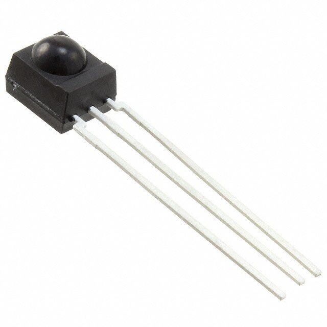
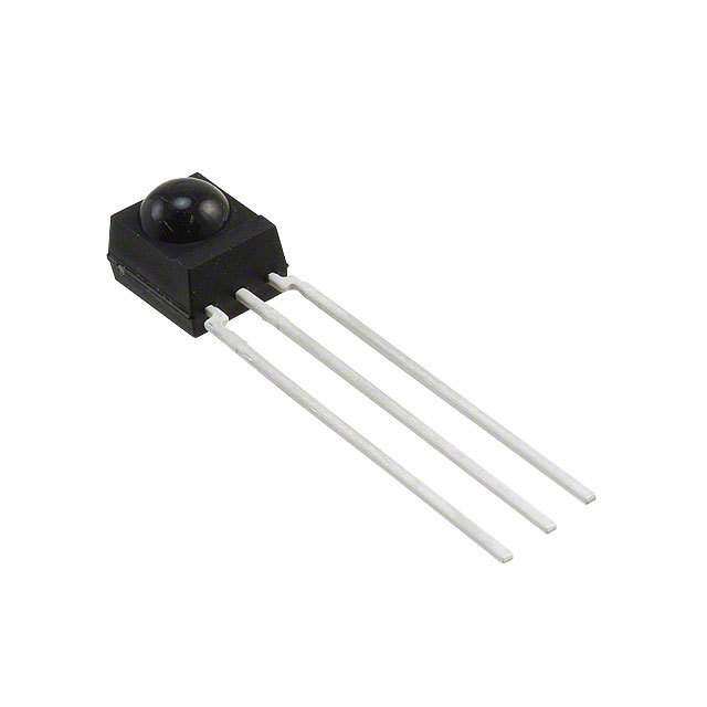
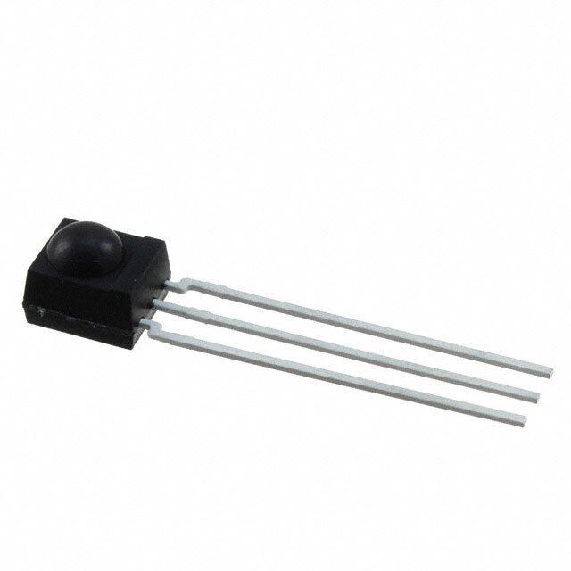
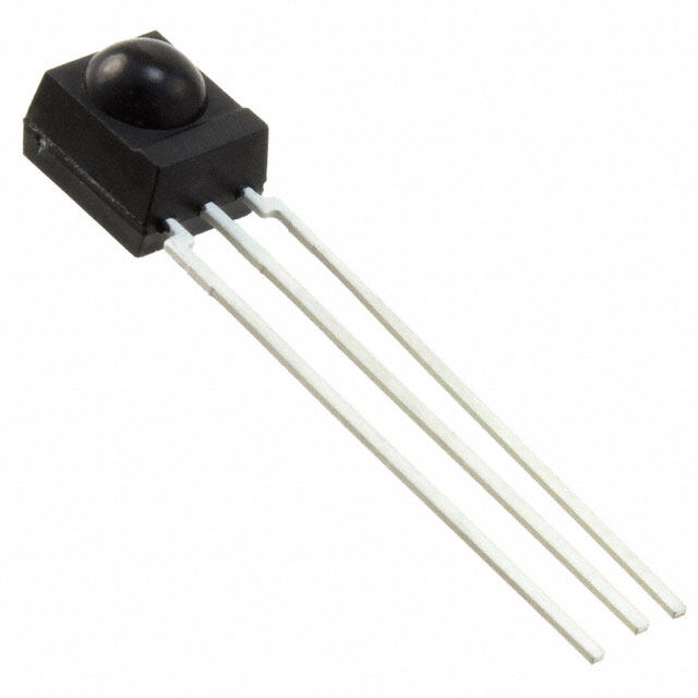
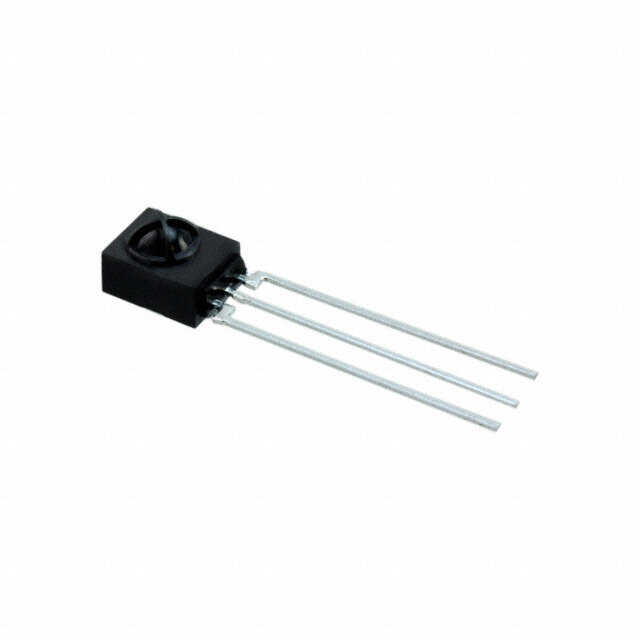
Vishay Semiconductor Opto Division的TSOP32236是一款红外遥控接收器,广泛应用于需要红外信号接收与解码的电子设备中。该器件集成了红外探测、放大、滤波和解调功能,能够有效识别标准红外遥控器发出的36kHz载波信号,具备良好的抗干扰能力和灵敏度。

其主要应用场景包括:

1. 家用电器:如电视机、机顶盒、空调、音响系统等,用于接收遥控器信号,实现远程控制功能。
2. 消费电子产品:如DVD播放器、投影仪、智能音箱等,作为人机交互的重要接口。
3. 自动化控制系统:在智能家居或工业控制系统中,用于接收红外指令,实现设备间的无线通信与控制。
4. 玩具与娱乐设备:遥控玩具车、游戏手柄等产品中,用作红外信号接收模块。
5. 安防设备:部分红外遥控门禁系统或监控设备中,用于接收控制信号。

TSOP32236采用小型化封装,便于集成于各类紧凑型设备中,且功耗低、可靠性高,适合电池供电设备使用。其内置屏蔽设计可有效防止环境光干扰,确保稳定工作。
| 参数 | 数值 |
| B.P.F.中心频率 | 36.0kHz |
| 产品目录 | |
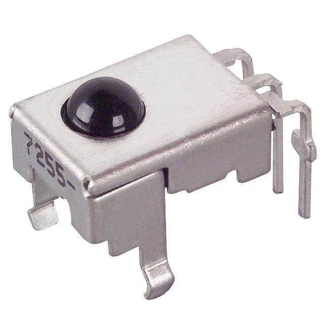
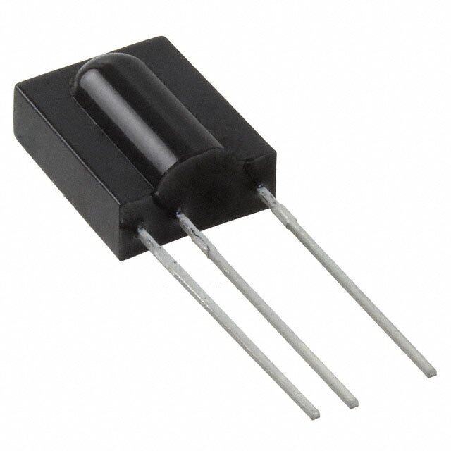
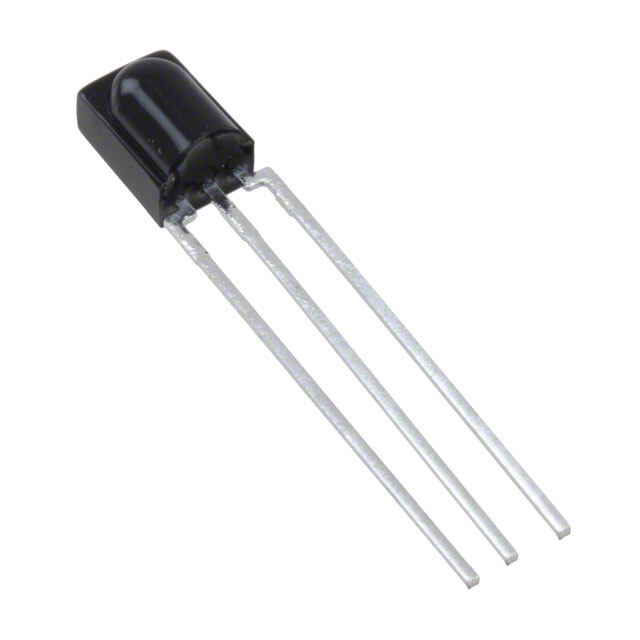
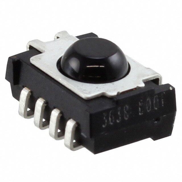
| 描述 | 3V PH.MODULE 36KHZ S.VIEW红外接收机 2.7-5.5V 36kHz |
| 产品分类 | |
| 品牌 | Vishay SemiconductorsVishay Semiconductor Opto Division |
| 产品手册 | |
| 产品图片 | |
| rohs | 符合RoHS无铅 / 符合限制有害物质指令(RoHS)规范要求 |
| 产品系列 | 红外接收机,Vishay Semiconductors TSOP32236- |
| 数据手册 | |
| 产品型号 | TSOP32236TSOP32236 |
| 产品种类 | Infrared Receiver Modules |
| 传输距离 | 45 m |
| 功率耗散 | 10 mW |
| 商标 | Vishay Semiconductors |
| 安装类型 | 通孔 |
| 安装风格 | Through Hole |
| 封装 | Tube |
| 射束角 | 45 deg |
| 工作电源电压 | 2.5 V to 5.5 V |
| 工厂包装数量 | 90 |
| 感应距离 | 45m |
| 数据传输速率 | 800 bits/s |
| 显示角 | 45 deg |
| 最大工作温度 | + 85 C |
| 最小工作温度 | - 25 C |
| 朝向 | 侧视图 |
| 标准包装 | 2,160 |
| 电压-电源 | 2.5 V ~ 5.5 V |
| 电流-电源 | 350µA |
| 电源电流 | 0.35 mA |
| 系列 | TSOP |
| 载频 | 36 kHz |
| 输出电流 | 5 mA |


- 商务部:美国ITC正式对集成电路等产品启动337调查
- 曝三星4nm工艺存在良率问题 高通将骁龙8 Gen1或转产台积电
- 太阳诱电将投资9.5亿元在常州建新厂生产MLCC 预计2023年完工
- 英特尔发布欧洲新工厂建设计划 深化IDM 2.0 战略
- 台积电先进制程称霸业界 有大客户加持明年业绩稳了
- 达到5530亿美元!SIA预计今年全球半导体销售额将创下新高
- 英特尔拟将自动驾驶子公司Mobileye上市 估值或超500亿美元
- 三星加码芯片和SET,合并消费电子和移动部门,撤换高东真等 CEO
- 三星电子宣布重大人事变动 还合并消费电子和移动部门
- 海关总署:前11个月进口集成电路产品价值2.52万亿元 增长14.8%
PDF Datasheet 数据手册内容提取
TSOP322.., TSOP324.., TSOP344.., TSOP348.. www.vishay.com Vishay Semiconductors IR Receiver Modules for Remote Control Systems FEATURES • Very low supply current • Photo detector and preamplifier in one package • Internal filter for PCM frequency • Supply voltage: 2.5 V to 5.5 V • Improved immunity against ambient light • Insensitive to supply voltage ripple and noise 1 • Material categorization: 22 for definitions of compliance please see 33 16672 www.vishay.com/doc?99912 DESIGN SUPPORT TOOLS click logo to get started DESCRIPTION The TSOP322.., TSOP348.., TSOP324.. and TSOP344.. Models series are miniaturized IR receiver modules for infrared Available remote control systems. A PIN diode and a preamplifier are assembled on lead frame, the epoxy package contains an IR MECHANICAL DATA filter. Pinning for TSOP348.., TSOP344..: The demodulated output signal can be directly connected to 1 = OUT, 2 = GND, 3 = V a microprocessor for decoding. S Pinning for TSOP322.., TSOP324..: The TSOP324.., TSOP344.. series devices are optimized 1 = OUT, 2 = V , 3 = GND to suppress almost all spurious pulses from energy saving S lamps like CFLs. The AGC4 used in the TSOP324.., TSOP344.. may suppress some data signals. The TSOP322.., TSOP348.. series are provided primarily for compatibility with old AGC2 designs. New designs should prefer the TSOP324.., TSOP344.. series containing the newer AGC4. These components have not been qualified according to automotive specifications. PARTS TABLE LEGACY, FOR RECOMMENDED FOR AGC LONG BURST REMOTE CONTROLS (AGC2) LONG BURST CODES (AGC4) 30 kHz TSOP34830 TSOP32230 TSOP34430 TSOP32430 33 kHz TSOP34833 TSOP32233 TSOP34433 TSOP32433 Carrier 36 kHz TSOP34836 TSOP32236 TSOP34436 (1)(2)(3) TSOP32436 (1)(2)(3) frequency 38 kHz TSOP34838 TSOP32238 TSOP34438 (4)(5) TSOP32438 (4)(5) 40 kHz TSOP34840 TSOP32240 TSOP34440 TSOP32440 56 kHz TSOP34856 TSOP32256 TSOP34456 (6)(7) TSOP32456 (6)(7) Package Mold Pinning 1 = OUT, 2 = GND, 3 = V 1 = OUT, 2 = V , 3 = GND 1 = OUT, 2 = GND, 3 = V 1 = OUT, 2 = V , 3 = GND S S S S Dimensions (mm) 6.0 W x 6.95 H x 5.6 D Mounting Leaded Application Remote control Best choice for (1) RC-5 (2) RC-6 (3) Panasonic (4) NEC (5) Sharp (6) r-step (7) Thomson RCA Rev. 1.6, 24-Sep-2018 1 Document Number: 82489 THIS DOCUMENT IS SUBJECT TO CHANGE WITHOUT NOTICE. THE PRODUCTS DESCRIBED HEREIN AND THIS DOCUMENT ARE SUBJECT TO SPECIFIC DISCLAIMERS, SET FORTH AT www.vishay.com/doc?91000
TSOP322.., TSOP324.., TSOP344.., TSOP348.. www.vishay.com Vishay Semiconductors BLOCK DIAGRAM APPLICATION CIRCUIT 16833-13 17170-11 3 R1 Transmitter IR receiver 30 kΩ TSAwLitxhxxx VS + VS 1 uit C1 c μC Input AGC Band Demo- Cir OUT pass dulator V GND O GND 2 PIN Control circuit R and C recommended to reduce supply ripple for V < 2.8 V 1 1 S ABSOLUTE MAXIMUM RATINGS PARAMETER TEST CONDITION SYMBOL VALUE UNIT Supply voltage V -0.3 to +6 V S Supply current I 3 mA S Output voltage V -0.3 to (V + 0.3) V O S Output current I 5 mA O Junction temperature T 100 °C j Storage temperature range T -25 to +85 °C stg Operating temperature range T -25 to +85 °C amb Power consumption T ≤ 85 °C P 10 mW amb tot Soldering temperature t ≤ 10 s, 1 mm from case T 260 °C sd Note • Stresses beyond those listed under “Absolute Maximum Ratings” may cause permanent damage to the device. This is a stress rating only and functional operation of the device at these or any other conditions beyond those indicated in the operational sections of this specification is not implied. Exposure to absolute maximum rating conditions for extended periods may affect the device reliability ELECTRICAL AND OPTICAL CHARACTERISTICS (T = 25 °C, unless otherwise specified) amb PARAMETER TEST CONDITION SYMBOL MIN. TYP. MAX. UNIT E = 0, V = 3.3 V I 0.27 0.35 0.45 mA v S SD Supply current E = 40 klx, sunlight I - 0.45 - mA v SH Supply voltage V 2.5 - 5.5 V S E = 0, test signal see Fig. 1, v Transmission distance IR diode TSAL6200, d - 30 - m I = 50 mA F I = 0.5 mA, E = 0.7 mW/m2, Output voltage low OSL e V - - 100 mV test signal see Fig. 1 OSL Pulse width tolerance: Minimum irradiance t - 5/f < t < t + 6/f , E - 0.08 0.15 mW/m2 pi 0 po pi 0 e min. test signal see Fig. 1 t - 5/f < t < t + 6/f , Maximum irradiance pi 0 po pi 0 E 30 - - W/m2 test signal see Fig. 1 e max. Directivity Angle of half transmission ϕ - ± 45 - ° distance 1/2 Rev. 1.6, 24-Sep-2018 2 Document Number: 82489 THIS DOCUMENT IS SUBJECT TO CHANGE WITHOUT NOTICE. THE PRODUCTS DESCRIBED HEREIN AND THIS DOCUMENT ARE SUBJECT TO SPECIFIC DISCLAIMERS, SET FORTH AT www.vishay.com/doc?91000
TSOP322.., TSOP324.., TSOP344.., TSOP348.. www.vishay.com Vishay Semiconductors TYPICAL CHARACTERISTICS (T = 25 °C, unless otherwise specified) amb Ee Optical Test Signal 0.8 (IR diode TSAL6200, IF = 0.4 A, 30 pulses, f = f0, t = 10 ms) t s) 0.7 on m dth ( 0.6 t e Wi 0.5 tpi * Puls 0.4 toff T ut * tpi 10/f0 is recommended for optimal function Outp 0.3 VVOOH Output S12i))g 7tnp/ifa 0-l <5/ ft0d << t1p5o /<f0 tpi + 6/f0 16110 t, t - onoff 00..201 opticalλ t e=s t9 s5i0g nnaml,, fig. 3 0.1 1 10 100 1000 10 000 V OL td1) tpo2) t 20744 Ee - Irradiance (mW/m²) Fig. 1 - Output Active Low Fig. 4 - Output Pulse Diagram 1.0 1.2 ms) 00..89 Output pulse width nsivity 1.0 Width ( 0.7 Input burst length Respo 0.8 ulse 00..56 ative 0.6 P el t - Output po 0000....1234 Opticaλl t=e s9t5 s0ig nnmal,, fig. 1 E/E - Re min.e 00..24 Δf(f3 = d fB0 )± = 5 f 0%/10 0 0.0 0.1 1 10 100 1000 10 000 0.7 0.9 1.1 1.3 20743 Ee - Irradiance (mW/m²) 16925 f/f0 - Relative Frequency Fig. 2 - Pulse Length and Sensitivity in Dark Ambient Fig. 5 - Frequency Dependence of Responsivity Ee Optical Test Signal W/m²) 34..50 C10o rWre/lmat²io =n 1w.4it hk laxm (sbtide.n itll uligmh.t As,o Tu r=ce 2s8:55 K) m 10 W/m² = 8.2 klx (daylight, T = 5900 K) e ( 3.0 c n Wavelength of ambient 600µs 600µs t adia 2.5 illumination: λ = 950 nm t = 60 ms hold Irr 12..50 VO Output Signal, (see Fig. 4) 94 8134 Thres 1.0 VOH - min. 0.5 Ee 0 VOL 0.01 0.1 1 10 100 ton toff t E - Ambient DC Irradiance (W/m²) 20745 e Fig. 3 - Output Function Fig. 6 - Sensitivity in Bright Ambient Rev. 1.6, 24-Sep-2018 3 Document Number: 82489 THIS DOCUMENT IS SUBJECT TO CHANGE WITHOUT NOTICE. THE PRODUCTS DESCRIBED HEREIN AND THIS DOCUMENT ARE SUBJECT TO SPECIFIC DISCLAIMERS, SET FORTH AT www.vishay.com/doc?91000
TSOP322.., TSOP324.., TSOP344.., TSOP348.. www.vishay.com Vishay Semiconductors Axis Title 2m) 3.0 1.0 10000 W/ y 0.9 m 2.5 vit hreshold Irradiance ( 112...050 ffff ==== 31f10000 0kk HHHzzz 2nd lineRelative Spectral Sensiti 000000......345678 1100000 1st line2nd line E - Te min. 0.50 λS()-rel. 00..12 1 10 100 1000 0 10 ΔV - AC Voltage on DC Supply Voltage (mV) 750 850 950 1050 1150 SRMS 21425 λ-Wavelength (nm) Fig. 7 - Sensitivity vs. Supply Voltage Disturbances Fig. 10 - Relative Spectral Sensitivity vs. Wavelength 0° 10° 20° 1.0 30° 0.9 e cl 0.8 y C y 0.7 40° ut D 0.6 1.0 e TSOP322.. velop 00..45 TSOP324.. TSOP348.. 0.9 50° En TSOP344.. 0.8 60° x. 0.3 Ma 0.2 70° 0.7 0.1 80° f = 38 kHz, E = 2 mW/m² e 0 0 20 40 60 80 100 120 0.6 0.4 0.2 0 20748-2 Burst Length (number of cycles/burst) 96 12223p2 drel - Relative Transmission Distance Fig. 8 - Max. Envelope Duty Cycle vs. Burst Length Fig. 11 - Horizontal Directivity 2m) 0.20 0.20 mW/ 00..1168 2m) 00..1168 ce ( 0.14 mW/ 0.14 n adia 0.12 vity ( 0.12 hold Irr 00..0180 Sensiti 00..0180 hres 00..0046 - min. 00..0046 E - Te min. 0.020-30 -10 10 30 50 70 90 Ee 00..0002 1 2 3 4 5 T - Ambient Temperature (°C) V - Supply Voltage (V) amb S Fig. 9 - Sensitivity vs. Ambient Temperature Fig. 12 - Sensitivity vs. Supply Voltage Rev. 1.6, 24-Sep-2018 4 Document Number: 82489 THIS DOCUMENT IS SUBJECT TO CHANGE WITHOUT NOTICE. THE PRODUCTS DESCRIBED HEREIN AND THIS DOCUMENT ARE SUBJECT TO SPECIFIC DISCLAIMERS, SET FORTH AT www.vishay.com/doc?91000
TSOP322.., TSOP324.., TSOP344.., TSOP348.. www.vishay.com Vishay Semiconductors SUITABLE DATA FORMAT Axis Title This series is designed to suppress spurious output pulses 7 10000 due to noise or disturbance signals. The devices can distinguish data signals from noise due to differences in 6 frequency, burst length, and envelope duty cycle. The data signal should be close to the device’s band-pass center de 5 1000 u fbWreehlqoeuwne .an cdya t(ea. gsi.g 3n8a lk iHs za)p apnlide dfu tlofi ltl hteh ep rcoodnudcitti oinn tsh ien pthrees teanbclee 2nd linenal Amplit 34 1st line2nd line g of a disturbance, the sensitivity of the receiver is Si 100 R 2 automatically reduced by the AGC to insure that no spurious I pulses are present at the receiver’s output. Some examples 1 which are suppressed are: 0 10 • DC light (e.g. from tungsten bulbs sunlight) 0 5 10 15 20 • Continuous signals at any frequency 16920 Time (ms) • Strongly or weakly modulated patterns from fluorescent Fig. 13 - IR Disturbance from Fluorescent Lamp lamps with electronic ballasts (see Fig. 13 or Fig. 14). With Low Modulation Axis Title 40 10000 20 e d 1000 u 2nd linegnal Amplit -200 1st line2nd line Si 100 R I -40 -60 10 0 5 10 15 20 16921 Time (ms) Fig. 14 - IR Disturbance from Fluorescent Lamp With High Modulation TSOP322.., TSOP348.. TSOP324.., TSOP344.. Minimum burst length 10 cycles/burst 10 cycles/burst After each burst of length 10 to 70 cycles 10 to 35 cycles a minimum gap time is required of ≥ 10 cycles ≥ 10 cycles For bursts greater than 70 cycles 35 cycles a minimum gap time in the data stream is needed of > 4 x burst length > 10 x burst length Maximum number of continuous short bursts/second 1800 1500 NEC code Yes Preferred RC5/RC6 code Yes Preferred Thomson 56 kHz code Yes Preferred Sharp code Yes Preferred Mild disturbance patterns Complex and critical disturbance patterns Suppression of interference from fluorescent lamps are suppressed (example: are suppressed (example: signal pattern signal pattern of Fig. 13) of Fig. 14 or highly dimmed LCDs) Notes • For data formats with short bursts please see the datasheet for TSOP323.., TSOP325.., TSOP343.., TSOP345.. • For Sony 12, 15, and 20 bit IR codes please see the datasheet of TSOP34S40F, TSOP32S40F Rev. 1.6, 24-Sep-2018 5 Document Number: 82489 THIS DOCUMENT IS SUBJECT TO CHANGE WITHOUT NOTICE. THE PRODUCTS DESCRIBED HEREIN AND THIS DOCUMENT ARE SUBJECT TO SPECIFIC DISCLAIMERS, SET FORTH AT www.vishay.com/doc?91000
TSOP322.., TSOP324.., TSOP344.., TSOP348.. www.vishay.com Vishay Semiconductors PACKAGE DIMENSIONS in millimeters 3.9 6 3 5. 5 9 25 6. 8. 5) 5 5. ( 5 0. ± 5 30. 1 0.85 max. 1 0.89 0.5 max. 2.54 nom. 1.3 0.7 max. 4.1 2.54 nom. 5.6 marking area Not indicated tolerances ± 0.2 technical drawings according to DIN specifications R 2.5 Drawing-No.: 6.550-5169.01-4 Issue: 9; 03.11.10 13655 Rev. 1.6, 24-Sep-2018 6 Document Number: 82489 THIS DOCUMENT IS SUBJECT TO CHANGE WITHOUT NOTICE. THE PRODUCTS DESCRIBED HEREIN AND THIS DOCUMENT ARE SUBJECT TO SPECIFIC DISCLAIMERS, SET FORTH AT www.vishay.com/doc?91000
Legal Disclaimer Notice www.vishay.com Vishay Disclaimer ALL PRODUCT, PRODUCT SPECIFICATIONS AND DATA ARE SUBJECT TO CHANGE WITHOUT NOTICE TO IMPROVE RELIABILITY, FUNCTION OR DESIGN OR OTHERWISE. Vishay Intertechnology, Inc., its affiliates, agents, and employees, and all persons acting on its or their behalf (collectively, “Vishay”), disclaim any and all liability for any errors, inaccuracies or incompleteness contained in any datasheet or in any other disclosure relating to any product. Vishay makes no warranty, representation or guarantee regarding the suitability of the products for any particular purpose or the continuing production of any product. To the maximum extent permitted by applicable law, Vishay disclaims (i) any and all liability arising out of the application or use of any product, (ii) any and all liability, including without limitation special, consequential or incidental damages, and (iii) any and all implied warranties, including warranties of fitness for particular purpose, non-infringement and merchantability. Statements regarding the suitability of products for certain types of applications are based on Vishay’s knowledge of typical requirements that are often placed on Vishay products in generic applications. Such statements are not binding statements about the suitability of products for a particular application. It is the customer’s responsibility to validate that a particular product with the properties described in the product specification is suitable for use in a particular application. Parameters provided in datasheets and / or specifications may vary in different applications and performance may vary over time. All operating parameters, including typical parameters, must be validated for each customer application by the customer’s technical experts. Product specifications do not expand or otherwise modify Vishay’s terms and conditions of purchase, including but not limited to the warranty expressed therein. Except as expressly indicated in writing, Vishay products are not designed for use in medical, life-saving, or life-sustaining applications or for any other application in which the failure of the Vishay product could result in personal injury or death. Customers using or selling Vishay products not expressly indicated for use in such applications do so at their own risk. Please contact authorized Vishay personnel to obtain written terms and conditions regarding products designed for such applications. No license, express or implied, by estoppel or otherwise, to any intellectual property rights is granted by this document or by any conduct of Vishay. Product names and markings noted herein may be trademarks of their respective owners. © 2017 VISHAY INTERTECHNOLOGY, INC. ALL RIGHTS RESERVED Revision: 08-Feb-17 1 Document Number: 91000