ICGOO在线商城 > 传感器,变送器 > 光学传感器 - 光电检测器 - 遥控接收器 > RPM7238-H8R
 Datasheet下载
- 型号: RPM7238-H8R
- 制造商: ROHM Semiconductor
- 库位|库存: xxxx|xxxx
- 要求:
| 数量阶梯 | 香港交货 | 国内含税 |
| +xxxx | $xxxx | ¥xxxx |
查看当月历史价格
查看今年历史价格
RPM7238-H8R产品简介:
ICGOO电子元器件商城为您提供RPM7238-H8R由ROHM Semiconductor设计生产,在icgoo商城现货销售,并且可以通过原厂、代理商等渠道进行代购。 RPM7238-H8R价格参考。ROHM SemiconductorRPM7238-H8R封装/规格:光学传感器 - 光电检测器 - 遥控接收器, Remote Receiver Sensor, 37.9kHz 15m Through Hole。您可以下载RPM7238-H8R参考资料、Datasheet数据手册功能说明书,资料中有RPM7238-H8R 详细功能的应用电路图电压和使用方法及教程。
Rohm Semiconductor的RPM7238-H8R是一款红外遥控接收器,广泛应用于消费电子和家用电器领域。以下是其主要应用场景:

1. 电视与显示器:作为电视或显示器的核心组件之一,RPM7238-H8R负责接收来自遥控器的红外信号,实现频道切换、音量调节、输入源选择等功能。

2. 空调与家电控制:在空调、风扇、加湿器等家用设备中,该器件用于接收用户通过遥控器发出的温度设置、模式切换、定时开关等指令。

3. 音响系统:支持家庭影院、蓝牙音箱等音频设备的无线操控,例如播放/暂停、曲目切换及音效调整。

4. 机顶盒与流媒体设备:适用于有线电视、卫星接收器或智能流媒体播放器,提供便捷的内容浏览与菜单导航功能。

5. 智能家居设备:可用于智能灯泡、窗帘、安防摄像头等物联网产品中,实现远程控制和自动化操作。

6. 工业与商用设备:如投影仪、数字标牌、自动售货机等场合,可简化人机交互过程,提升用户体验。

RPM7238-H8R具有高灵敏度、低功耗以及较强的抗干扰能力,能够在复杂环境中稳定工作。同时,其紧凑的设计便于集成到各类小型化电子产品中,满足现代设备对空间优化的需求。
| 参数 | 数值 |
| B.P.F.中心频率 | 37.9kHz |
| 产品目录 | |
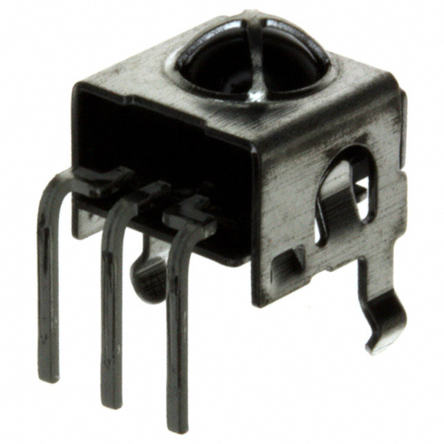
| 描述 | RECEIVER REMOTE CTRL 37.9KHZ TOP红外接收机 REMOTE CTRL 37.9KHZ |
| 产品分类 | |
| 品牌 | ROHM Semiconductor |
| 产品手册 | |
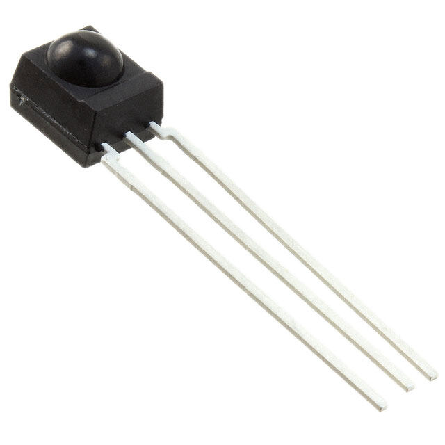
| 产品图片 |
|
| rohs | 符合RoHS无铅 / 符合限制有害物质指令(RoHS)规范要求 |
| 产品系列 | 红外接收机,ROHM Semiconductor RPM7238-H8RRPM7238-R |
| 数据手册 | |
| 产品型号 | RPM7238-H8R |
| 产品种类 | 红外接收机 |
| 传输距离 | 15 m |
| 低电平脉冲宽度 | 800 us |
| 其它名称 | RPM7238H8R |
| 商标 | ROHM Semiconductor |
| 安装类型 | 通孔 |
| 封装 | Bulk |
| 封装/箱体 | RSIP-A3 |
| 工作电源电压 | 2.7 V to 3.6 V |
| 工厂包装数量 | 1000 |
| 感应距离 | 15m |
| 显示角 | 45 deg, 35 deg |
| 最大工作温度 | + 75 C |
| 最小工作温度 | - 10 C |
| 最小高电平输出电压 | 2.5 V |
| 朝向 | 顶视图 |
| 标准包装 | 1,000 |
| 电压-电源 | 2.7 V ~ 3.6 V |
| 电流-电源 | 500µA |
| 电源电流 | 300 uA |
| 载频 | 37.9 kHz |
| 输出电流 | 2 mA |
| 高电平脉冲宽度 | 800 us |


- 商务部:美国ITC正式对集成电路等产品启动337调查
- 曝三星4nm工艺存在良率问题 高通将骁龙8 Gen1或转产台积电
- 太阳诱电将投资9.5亿元在常州建新厂生产MLCC 预计2023年完工
- 英特尔发布欧洲新工厂建设计划 深化IDM 2.0 战略
- 台积电先进制程称霸业界 有大客户加持明年业绩稳了
- 达到5530亿美元!SIA预计今年全球半导体销售额将创下新高
- 英特尔拟将自动驾驶子公司Mobileye上市 估值或超500亿美元
- 三星加码芯片和SET,合并消费电子和移动部门,撤换高东真等 CEO
- 三星电子宣布重大人事变动 还合并消费电子和移动部门
- 海关总署:前11个月进口集成电路产品价值2.52万亿元 增长14.8%
PDF Datasheet 数据手册内容提取
SERIES CATALOG Photo Link Modules Remote Control Receiver Module IrDA Infrared Communication Module
e ul d o M RReemmoottee CCoonnttrrooll RReecceeiivveerr MMoodduullee r e v ei c e R ol r t n o C e t o m e R Remote Control Receiver Module (cid:1) Contents Remote Control Receiver Module Selection Guide................................................... 1 RPM7200 Series ............................................................................................................. 3 RPM7100 Series ............................................................................................................. 5 External Dimensions....................................................................................................... 7 Basic Knowledge of Remote Control ........................................................................... 9 Remote Control Receiver Module and Data Communication.................................. 10 Block Diagram and Work of Remote Control Receiver Module .............................. 11 Remote Control Transmission Signal .......................................................................... 13 Precautions for Designing Transmitter Side ............................................................... 15 Precautions for Designing Receiver Side ................................................................... 17 Receiving Discrimination Method to Expand Effective Distance............................. 21 Measures for Preventing Malfunctions ........................................................................ 22
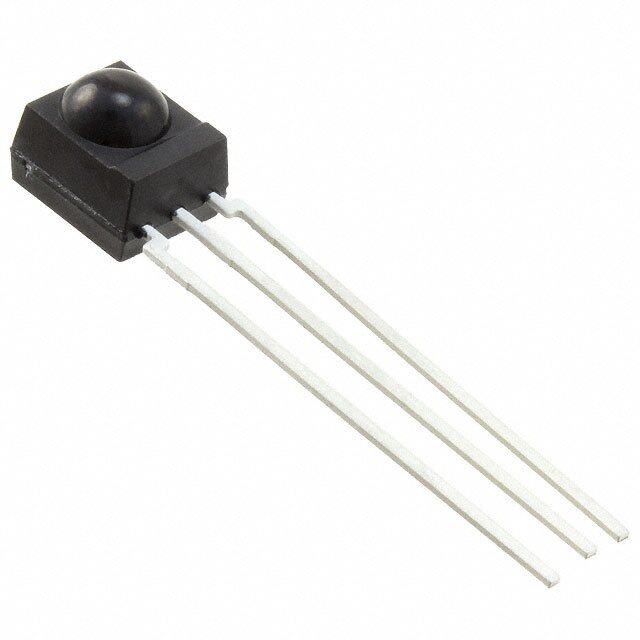
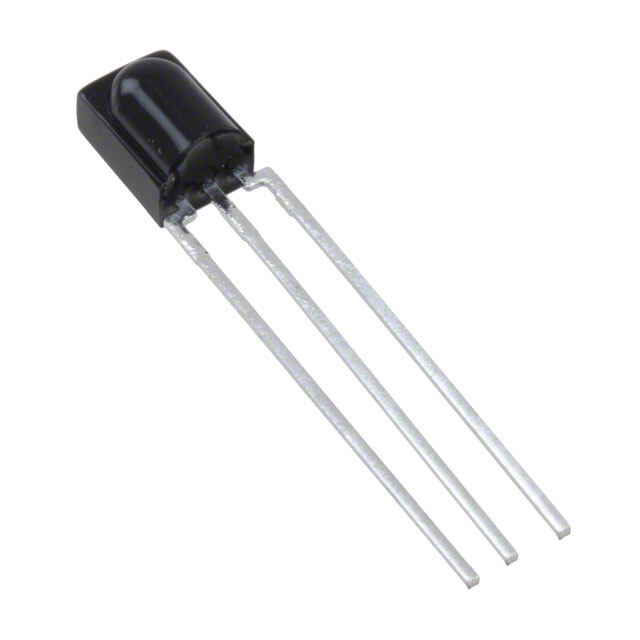
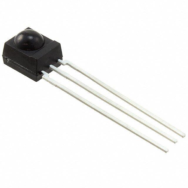
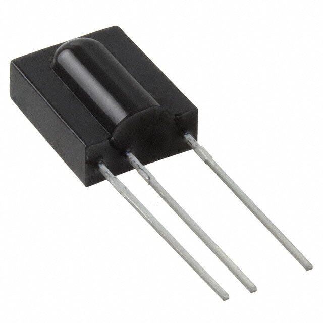
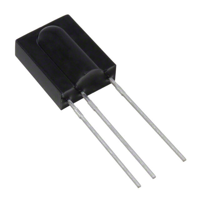
Remote Control Receiver Module (cid:1) Remote Control Receiver Module Selection Guide Remote Control Receiver Module (at 3.0 to 3.3V) R 36.0kHz RPM7236-H5 9.6mm 36.7kHz RPM7237-H5 Carrier frequency 37.9kHz RPM7238-H5 40.0kHz RPM7240-H5 Distance from PCB to lens 36.0kHz 15.0mm RPM7236-H13 36.7kHz RPM7237-H13 SIDE VIEW Carrier frequency 37.9kHz RPM7238-H13 40.0kHz RPM7240-H13 36.0kHz Shape RPM7236-H8 7.2mm 36.7kHz RPM7237-H8 Carrier frequency 37.9kHz RPM7238-H8 40.0kHz RPM7240-H8 TOP VIEW 36.0kHz RPM7236-H9 12.0mm 36.7kHz Distance RPM7237-H9 Carrier from PCB frequency 37.9kHz to lens RPM7238-H9 40.0kHz RPM7240-H9 36.0kHz RPM7236-H4 15.9mm 36.7kHz RPM7237-H4 Carrier frequency 37.9kHz RPM7238-H4 40.0kHz RPM7240-H4 1
Remote Control Receiver Module Selection Guide e Remote Control Receiver Module (at 5.0V) ul d o M 5.5mm 36.0kHz RPM7136 er v 36.7kHz RPM7137 ei c Carrier 37.9kHz RPM7138 Re frequency 40.0kHz ol RPM7140 tr n 56.9kHz o RPM7157 C e 36.0kHz ot RPM7136-H5 m 9.6mm 36.7kHz e R RPM7137-H5 Distance Carrier 37.9kHz from PCB RPM7138-H5 frequency to lens 40.0kHz RPM7140-H5 3 56.9kHz RPM7157-H5 36.0kHz 3 SIDE VIEW RPM7136-H13 15.0mm 36.7kHz RPM7137-H13 3 Carrier 37.9kHz RPM7138-H13 frequency 3 40.0kHz RPM7140-H13 56.9kHz RPM7157-H13 Shape 36.0kHz RPM7136-V4 4.8mm 36.7kHz RPM7137-V4 Carrier 37.9kHz RPM7138-V4 frequency 40.0kHz RPM7140-V4 56.9kHz RPM7157-V4 36.0kHz RPM7136-H8 7.2mm 36.7kHz TOP VIEW RPM7137-H8 Carrier 37.9kHz RPM7138-H8 frequency 40.0kHz RPM7140-H8 56.9kHz Distance RPM7157-H8 from PCB 36.0kHz to lens RPM7136-H9 12.0mm 36.7kHz RPM7137-H9 Carrier 37.9kHz RPM7138-H9 frequency 40.0kHz RPM7140-H9 56.9kHz RPM7157-H9 36.0kHz RPM7136-H4 15.9mm 36.7kHz RPM7137-H4 Carrier 37.9kHz RPM7138-H4 frequency 40.0kHz RPM7140-H4 56.9kHz RPM7157-H4 2
Remote Control Receiver Module (cid:1) (cid:1) Electrical and Optical Characteristics of RPM7200 Series T Absolute Maximum Ratings (Ta=25°C) Parameter Symbol Limits Unit Supply Voltage V 6.3 V CC B) Storage Temperature Range Tstg -30~+100 °C n (d Operating Temperature Range Topr -10~+75 °C ai G Solder Temperature Tsol 260* °C * Within 5s and 3mm of the route of the lead. - Recommended Operating Conditions (Ta=25°C) Parameter Symbol Min. Typ. Max. Unit Supply Voltage VCC 2.7 3.0 3.6 V %) e (1 c n a st di Electrical Characteristics (Ta=25°C and Vcc=3V unless otherwise specified) e v cti Parameter Symbol Min. Typ. Max. Unit Conditions e eff Current Consumption Icc 0.3 0.5 mA With no external light or input e v Effective Distance on Axis L 8 15 m *1 External light condition Ee<10 lx elati R High Level Output Voltage VH 2.5 V *1 Low Level Output Voltage VL 0.5 V *1 Isink=200µA max. ON Pulse Width TON 400 600 800 µs *1 External light condition Ee<10 lx OFF Pulse Width TOFF 400 600 800 µs *1 External light condition Ee<10 lx Horizontal Half Angle θ1/2 45 deg *2 Vertical Half Angle θ1/2 35 deg *2 *1. Burst waves (600/600µs) are transmitted by a standard transmitter, and the 100th and later pulses are measured. *2. A directional angle where the effective distance is half the linear arrival distance. Shape Side View Top View Package RSIP-A3 (H5) RSIP-A3 (H13) RSIP-A3 (H8) RSIP-A3 (H9) RSIP-A3 (H4) Hight (PCB to LENS) 9.6mm 15.0mm 7.2mm 12.0mm 15.9mm Carrier Frequency 36.0kHz RPM7236-H5 RPM7236-H13 RPM7236-H8 RPM7236-H9 RPM7236-H4 36.7kHz RPM7237-H5 RPM7237-H13 RPM7237-H8 RPM7237-H9 RPM7237-H4 37.9kHz RPM7238-H5 RPM7238-H13 RPM7238-H8 RPM7238-H9 RPM7238-H4 40.0kHz RPM7240-H5 RPM7240-H13 RPM7240-H8 RPM7240-H9 RPM7240-H4 3
RPM7200 Series (cid:1) s Typical Characteristics of RPM7200 Series 120 ule 0.00 %)100 od -2.00 vity ( 80 er M n (dB) -4.00 sensiti 60 eceiv Gai --68..0000 Relative 2400 ntrol R o C -10.00 0 e -8 -7 -6 -5 -4 -3 -2 -1 fo +1 +2 +3 +4 +5 +6 +7 +8 700 750 800 850 900 950 1000 1050 1100 t o Frequency (kHz) Wavelength: λ (nm) m BPF characteristics Spectral sensitivity characteristics (Photodiode) e R %) %) e (100 e (100 c c n n a 80 a 80 st st di di e 60 e 60 v v cti cti e 40 e 40 eff eff ve 20 ve 20 lx elati 0 elati 0 R -80 -60 -40 -20 0 20 40 60 80 R -80 -60 -40 -20 0 20 40 60 80 Angle (°) Angle (°) Directional characteristics (Horizontal) Directional characteristics (Vertical) lx lx 4
Remote Control Receiver Module (cid:1) (cid:1) Electrical and Optical Characteristics of RPM7100 Series Absolute Maximum Ratings (Ta=25°C) Parameter Symbol Limits Unit Supply voltage VCC 6.3 V B) Storage Temperature Range Tstg -30~+100 °C n (d Operating Temperature Range Topr -10~+75 °C Gai Solder Temperature Tsol 260* °C * Within 5s and 3mm of the route of the lead. - Recommended Operating Conditions (Ta=25°C) Parameter Symbol Min. Typ. Max. Unit Supply Voltage VCC 4.5 5.0 5.5 V %) e ( c n a st Electrical Characteristics (Ta=25°C and Vcc=5V unless otherwise specified) e di v Parameter Symbol Min. Typ. Max. Unit Conditions ecti eff Current Consumption Icc 0.95 1.5 mA With no external light or input e v Effective Distance on Axis L 8 15 m *1 External light condition Ee<10 lx ati el High Level Output Voltage VH 4.5 V *1 R Low Level Output Voltage VL 0.5 V *1 Isink=200µA max. ON Pulse Width TON 400 600 800 µs *1 External light condition Ee<10 lx OFF Pulse Width TOFF 400 600 800 µs *1 External light condition Ee<10 lx Horizontal Half Angle θ1/2 45 deg *2 Vertical Half Angle θ1/2 35 deg *2 *1. Burst waves (600/600µs) are transmitted by a standard transmitter, and the 100th and later pulses are measured. *2. A directional angle where the effective distance is half the linear arrival distance. Shape Side View Top View Package RSIP-A3 RSIP-A3 (H5)RSIP-A3 (H13) RSIP-A3 V4 RSIP-A3 (H8)RSIP-A3 (H9)RSIP-A3 (H4) Hight (PCB to LENS) 5.5mm 9.6mm 15.0mm 4.8mm 7.2mm 12.0mm 15.9mm Carrier Frequency 36.0kHz RPM7136 RPM7136-H5 RPM7136-H13 RPM7136-V4 RPM7136-H8 RPM7136-H9 RPM7136-H4 36.7kHz RPM7137 RPM7137-H5 RPM7137-H13 RPM7137-V4 RPM7137-H8 RPM7137-H9 RPM7137-H4 37.9kHz RPM7138 RPM7138-H5 RPM7138-H13 RPM7138-V4 RPM7138-H8 RPM7138-H9 RPM7138-H4 40.0kHz RPM7140 RPM7140-H5 RPM7140-H13 RPM7140-V4 RPM7140-H8 RPM7140-H9 RPM7140-H4 56.9kHz RPM7157 RPM7157-H5 RPM7157-H13 RPM7157-V4 RPM7157-H8 RPM7157-H9 RPM7157-H4 5
RPM7100 Series (cid:1) s Typical Characteristics of RPM7100 Series 120 e ul 0.00 d %)100 o Gain (dB) ---246...000000 ative sensitivity ( 468000 rol Receiver M -8.00 Rel 20 ont C -10.00-8 -7 -6 -5 -4 -3 -2 -1 fo +1 +2 +3 +4 +5 +6 +7 +8 0700 750 800 850 900 950 1000 1050 1100 te Frequency (kHz) Wavelength: λ (nm) mo BPF characteristics Spectral sensitivity characteristics (Photodiode) e R %) %) e (100 e (100 c c an 80 an 80 st st e di 60 e di 60 v v ecti 40 ecti 40 eff eff e 20 e 20 v v 0 lx Relati 0-80 -60 -40 -20 0 20 40 60 80 Relati 0 -80 -60 -40 -20 0 20 40 60 80 Angle (°) Angle (°) Directional characteristics (Horizontal) Directional characteristics (Vertical) 0 lx 0 lx 4) H4 H4 H4 H4 H4 6
Remote Control Receiver Module (cid:1) External Dimensions (Unit: mm) (cid:2)RSIP-A3 (H13) (cid:2)RSIP-A3 (H4) 9.0 1.8 7.3 6.0 15.9 7.3 2.35 0.65 3.6 1.8 2.95 5 0 0.4 5 15.017.9 1.4 1.4 12.65 7. 9 7. 3.6 2.54 2.54 6 3. 4.2 4 2.5 (1) (2) (3) 0. (1) (2) (3) 1.4 4.6 0.5 0.6 1.4 6.3 0.6 0.6 5 54 0. 2. 6 0. 4 5 2. (cid:2)RSIP-A3 (H5) (cid:2)RSIP-A3 4.8 9.0 1.8 7.3 0.8 3.2 6.0 5 6.0 9 2. Max.6.50 0 4. 556 9. 1.5 2.3. 1 0.4 0.5 n. 3.6 1.0 22 Mi 0.4 0.5 2.5 0.6 0.6 1.4 4.6 (1) (2) (3) 2.542.54 1.4 6.3 (1) (2) (3) 4 5 2. 4 5 2. Pin number (1) Rout (2) GND (3) Vcc 7
External Dimensions e ul d o (cid:2)RSIP-A3 V4 (cid:2)RSIP-A3 (H8) M r e v ei c 7.30 e R ol 5 5 3.60 7.20 5 ntr 2.3 0.6 2.9 Co e 0.5 9.25 7.00 mot 0 0 e 1.4 1.4 3.60 0.50 R 0 4 4.8 0. 2.54 2.54 0.8 3.2 6.0 (1) (2) (3) 0 Max.6.54.0 0.60 1.80 0.4 9. 1.5 20.0 Min. 2.5 2.542.54 (1) (2) (3) 0 0 6 3 0. 0. (cid:2)RSIP-A3 (H9) 7.30 5 12.00 6 0. 35 3.60 95 2. 2. 0 0 5 7. 00 6 1.41.4 12. 0.50 3.60 0 2.54 2.54 4 0. (1) (2) (3) 0 0.6 1.80 0 0 6 3 0. 0. Pin number (1) Rout (2) GND (3) Vcc 8
Remote Control Receiver Module 1. Basic Knowledge of Remote Control 2 1) Remote Control Receiver Module 1) The Remote Control Receiver Module is an optical communications module that uses infrared rays for TV sets and audio equipment. Conventional models were of cubic structure (1.5 × 1.5cm) incorporating a PCB mounted with a PIN photodiode, receiver IC, and capacitors and covered with a shield casing. Since ROHM released a one-package model, however, mold resin models of one-package structure have been mainstream products. ROHM provides the RPM7100-Hx Series 120 RPM7200-Hx Series (operating at 5V) and the RPM7200-Hx Series (operating at 3.0V). Both of them are of two-chip e (%) 100 Competitors' C c 5-V products structure incorporating a PIN photodiode and an 80 st receiver IC. Di e v 60 ROHM's Remote Control Receiver Module cti e Eff prevents malfunctions caused by power line e 40 v noise by taking measures for a reduction in elati R 20 power supply ripples, thus suiting a variety of 2) power supply environments flexibly. 0 1 10 100 1000 10000 Ripple Frequency (kHz) Fig. 1 Relative Effective Distance vs. Power Supply Ripple Frequency of RPM7200-Hx 2) Remote Control Optical Signal The remote control uses an infrared optical signal. Infrared rays are invisible and longer in wavelength than visible light. Remote control models use a dominant wavelength around 950nm. 3) Reason for Use of Infrared Rays The remote control is overwhelmingly used indoors under light emitted from lighting apparatus, which includes quantities of visible light components. In order to prevent such light from becoming a noise source, the remote control uses infrared rays, which is rarely included in the light emitted 100 from the lighting apparatus. 80 In other words, the remote control uses infrared y (%) rays in order to improve the signal-to-noise ratio. sitivit 60 n e The RPM7100-Hx Series and RPM7200-Hx e s 40 v Series eliminate optical noise by providing the elati R 20 resin packages with a filter function that shuts off visible light. 0 40050060070080090010001100 Wavelength: λ (nm) Fig. 2 Relative Sensitivity of RPM7100-Hx/RPM7200-Hx 9
Basic Knowledge of Remote Control/Remote Control Receiver Module and Data Communication 2. Remote Control Receiver Module and Data Communication e 1) Structure of Remote Control Receiver Module ul d o M ays r e Holder casing v ei a Mold resin ec The photodiode and the signal processing IC R HM are die-bonded to the metal lead frame. Then ol r en nt Photodiode gold wires are bonded for necessary wiring. o C The parts are sealed with mold resin to shut e t o off visible optical noise, and the whole m e Signal processing IC structure except the condenser lens is covered R with a metal shield casing. Condenser lens Lead frame Fig. 3 Structure of RPM7100-Hx/RPM7200-Hx 2) Remote Control System Signal Flow 00 The Remote Control Receiver Module receives an optical signal from the Remote Control Unit and changes the signal into an electric signal. Press the Power ON button. (1) Infrared (3) Remote Control LED Receiver Module Instructions to Microcontroller electrical set Remote Control Unit (RPM7100-Hx) RPM7200-Hx us, LED turns ON (lit) at high level ng (2) Subcarrier (Ex. 36.7Hz, 38kHz, 40kHz) Electric signal generation (1) The Power-ON code Power-ON code signal is mixed with the subcarrier. Electric signal Optical signal 10
Remote Control Receiver Module 2) • (2)Optical signal Work of Optical signal Electric signal Remote Control Receiver Module Demodulation to (3)Electric signal the power-ON code signal. (The subcarrier is eliminated.) The level of output from the Remote Control Optical Module is low when the light is turned ON. The microcontroller performs code discrimination The set is and gives a power-ON instruction. turned ON. Fig. 4 3. Block Diagram and Work of Remote Control Receiver Module 1) Block Diagram of Remote Control Receiver Module VCC Amplifier Comparator RON B) d Photodiode ( IV BPF Detection i G GND RPM7100-Hx/RPM7200-Hx Fig. 5 Block Diagram 11
Remote Control Receiver Module and Data Communication/Block Diagram and Work of Remote Control Receiver Module e 2) Work of Each Blocks ul d o M r e v • Photodiode ei c e R The photodiode receives an optical signal transmitted from the remote control unit and ol r converts the optical signal into a current signal. The mold resin of the Remote Control Receiver nt o Module has a function to shut off visible light, thus allowing only the optical signal to pass. C e Figure 6 shows the spectral sensitivity characteristics of the mold resin and photodiode. ot m e R • IV The optical signal received by the photodiode and converted into the current signal is further ed.) converted into a voltage signal. An automatic gain control function is provided to suppress excessively strong optical signal input so that the signal will be within the permissible range of N. the circuits. • Amplifier 120 The IV block amplifies the voltage signal converted from the current signal to optimum %)100 amplitude for the later stages where the vity ( 80 signal is further processed. If the input is siti n 60 excessively high, the amplitude will be e s e limited in the IV block. v ati 40 le el R 20 0 700 750 800 850 900 950 1000 1050 1100 Wavelength: λ (nm) Fig. 6 Relative Spectral Sensitivity Characteristics of • BPF (Band Pass Filter) RPM7100-Hx/RPM7200-Hx C 0.00 The remote transmission signal is modulated -2.00 N B) by the subcarrier. The BPF is incorporated in d -4.00 ( order to extract only pure signal components n ai -6.00 from the signal (including noise) received. G ND -8.00 -10.00 -8 -7 -6 -5 -4 -3 -2 -1 fo +1 +2 +3 +4 +5 +6 +7+8 Frequency (kHz) Fig. 7 BPF Characteristics of RPM7100-Hx/RPM7200-Hx 12
Remote Control Receiver Module • Detection This block has a detector and integrator. The detector automatically determines the level of detection (a) according to the level of BPF output, and sets the timing of integration. BPF output (a) Detection «O Integral comparator (b) ROUT Fig. 8 Waveform Shaping of RPM7100-Hx/RPM7200-Hx Only the pure signal is extracted from the input signal that includes noise, at which time the level of detection is automatically adjusted according to the output amplitude of the BPF. • Comparator The output of the detection block is converted into a binary. The hysteresis (b) prevents chattering that results from noise. 4. Remote Control Transmission Signal Various methods are used for signal transmission, because there are no unified standards. The same PPM (pulse position modulation) code is used to discriminate 1 and 0 according to the pulse time interval. The amplitude of the subcarrier is modified according to the pulse train. Therefore, the subcarrier frequency range is between 33 and 57kHz. 13
Block Diagram and Work of Remote Control Receiver Module/Remote Control Transmission Signal “0” “1” e T T T 3T ul d o M r PF e v ei c e R ol r t n Subcarrier o C • • • 33~57kHz e t o m Fig. 9 e R «Overview of AEHA's (Association for Electric Home Appliances) Format» Application: Applicable to infrared remote control systems for home appliances with a subcarrier range up to 40kHz employed to transmit data. Subcarrier: 33kHz and 40kHz max. Signal format: A frame includes a leader, custom code, parity, data code, and trailer, the outline of which is shown below. Custom Parity Leader code Data code Trailer vel (a) Signal configuration 1 byte Leader “0” “1” Trailer (b) Pulse shape g 8T 4T T T T 3T T 8ms min. 0.35ms<T<0.5ms Fig. 10 In this format, the leader is used for the discrimination of the start of transmission, the custom code is registered and used to prevent the remote control and controlled equipment from malfunctioning, and the parity bit along with the custom code is used to confirm that the signal is addressed to the equipment in use. The trailer is used to discriminate the completion of t ransmission. With the diffusion of infrared remote control systems for home appliances, certain standards apply to each manufacturer's signal transmission method in the AEHA's format with the method officially registered, thus preventing the remote control and controlled equipment from he m alfunctioning. The transmission format presently in use takes individual measures for the prevention of se malfunctions. For example, a method is used to transmit the data code three times and read the data code only when the leader code is received correctly at least twice in the three ier transmissions. Another method is also used to transmit front and back signals and judge the data only after the front and back signals coincide. 14
Remote Control Receiver Module 5. Precautions for Designing Transmitter Side 1) Transmitter «Transmitter circuit example» The resister R is used to set the forward current LED current R of the LED and adjusts the optical output power Battery 100µ of the transmitter. LED The LED is used usually 5mm in diameter and of high-intensity type. (Optical wavelength (λ)=940 or 950nm) Sig The electrolytic capacitor C provides the LED current. Fig. 13 Precautions for Transmission Frequency Check that the subcarrier frequency of the transmitter coincides with the center frequency of the Remote Control Receiver Module, or otherwise the effective distance may be reduced or no receiving may be possible. 2) Transmission Format • Leader Pulse The Remote Control Receiver Module covers a wide input range, and automatically makes receiving sensitivity by using leader pulses. The pulse immediately after the start of input may fluctuate (i.e., the receiving pulse width of output may be wider than the transmission pulse width) if there is no leader pulse. Necessary time for sensitivity stabilization Signal Binary slice level Fig. 14 Automatic Sensitivity Adjustment 15
Precautions for Designing Transmitter Side e • Transmission Pulse Width ul d o M Specifications of output pulse width of Remote Control Receiver Module (Transmission pulse width: 600µs) r e v ei 600µs 600µs c ent e Output pulse MIN TYP MAX Unit R wer width ol Transmission r t TON/TOFF 400 600 800 µs on C e of t o m e R Receiving The receiving output pulse fluctuate ±200µs TON TOFF according to the transmission signal. ED Fig. 15 Transmission pulse width (ON/OFF): Both 200µs 200µs 200µs Transmission pulse cy be ON period OFF period Receiving pulse A dispersion range of ±200µs of the transmission signal Fig. 16 es In the worst case, the dispersion pulse range of output may be 0 to 400µs put and no receiving may be possible. on • Countermeasure against Dispersion of Receiving Output Pulses Take the transmission pulse width as wide as possible (for both ON and OFF periods) 1200 s) µ N ( 1000 O T h: 800 dt wi e 600 s ul p N 400 O ut p 200 ut O 0 0 200 400 600 800 1000 1200 Transmission burst length (µs) Fig. 17 Output ON Pulse Width vs. Transmission Burst Length of RPM7100-Hx/RPM7200-Hx 16
Remote Control Receiver Module 6. Precautions for Designing Receiver Side 1) Design of Beam Spread Angle • V • Installation of Sensor Window and Remote Control Receiver Module If the specified beam spread angle is θ1, design the sensor window to satisfy the following condition, as shown in the figure on the right-hand side: θ>θ1. If the angle is specified from the lens top, there will be no optical signal incidence at the edge of the lens. Therefore, the Remote Control Receiver Module will not fully demonstrate its performance. Remote Control Design the window at the angle Receiver Module connecting the lens edge and window edge. Fig. 18 Sensor Window of RPM7100-Hx/RPM7200-Hx • Light Guide Tube Apply the condition below, on the condition that the diameter of light guide tube on the Remote Control Receiver Module is φ1 and that of the lens of the Remote Control φ1 Receiver is φ2. φ1>φ2 The maximum sensitivity is obtained by Remote Control beaming the optical signal at the whole Receiver Module φ2 surface of the lens. Fig. 19 Light Guide Tube of RPM7100-Hx/RPM7200-Hx 2) Environment-resistive Noise Design Environments where the Remote Control Receiver Module is used have quantities of noise • sources. The Remote Control Receiver Module has very high sensitivity to receive minute optical signals. Therefore, the Remote Control Receiver Module takes a variety of countermeasures against each noise source. If there is an interference of excessive noise, however, the Remote Control Receiver Module may malfunction. 17
Precautions for Designing Receiver Side e • Various Types of Optical Noise ul d o 100 M r e v %) 80 cei haes ght source ( 60 Sunlight Incandescent Lamp ntrol Re of li Co ensity 40 ote ere n int em o R of ssi 20 Fluorescent Lamp mi ver E e. 0 0.2 0.5 1 2 3 4 Wavelength: λ (mm) Fig. 20 Optical Noise Wavelength Characteristics Rapid Fluorescent Lamp The light emission frequency of a standard fluorescent lamp is 100Hz or 120Hz in most of the countries. It depends on the goverment policy. Although the light emission frequency is sufficiently lower than the subcarrier frequency of the remote control, the harmonics may cause on a malfunction (i.e., a reduction in the effective distance may result). he nd High Frequency Modulation Type Fluorescent Lamp ol In order to reduce the flickering of light, the light emission frequency of an inverter fluorescent lamp is modified. The frequency is around 45kHz, which is close to the subcarrier of the remote controller and becomes noise that cannot be eliminated with ease. by With the incidence of inverter fluorescent light, the effective distance will be shorter in le comparison with the case of the rapid fluorescent lamp. Incandescent Lamp and Sunlight These light sources have DC noise but including a large quantity of infrared components used for the remote control. The incidence of the noise results in a reduction in effective distance. se • Countermeasures of Set for Optical Noise ute of Lighting apparatus becomes an optical noise source. In many cases, this noise source is se, radiated from the upper side. Therefore, at the time of designing the window of the set, limit the incidence of light from the upper side. 18
Remote Control Receiver Module • Other Noise Sources • H Power Supply Noise Power supply noise may wrap around from the digital block of the set or may result due to the insufficient smoothing of the power supply circuit. If there are power supply ripples, the effective distance may be reduced. The RPM7100-Hx and RPM7200-Hx Series are designed to reduce the droppage of effective distance to the minimum. Electromagnetic Noise The following ones may be sources of electromagnetic noise. • CRT noise • LCD (driver) noise (i.e., horizontal synchronizing signal at 38kHz) • Fluorescent lamp • Noise radiated from power supply circuit 3) Grounding and Pattern Designing • V • Output pull-up resistance «Circuit diagram» R C + Vcc 47µF ROUT Microcontroller GND Fig. 21 Pull-up Circuit Diagram The pull-up resistance connected to the output must limit the absorption current of Remote Control Receiving Module to a range not exceeding a specified value, or otherwise the low-level voltage will be in excess of the specified value. Isink: Specified Absorption Current Max. Vcc-VOL Model Isink (µA) R> RPM7100-Hx Series 400 Isink RPM7200-Hx Series 200 19
Precautions for Designing Receiver Side e • Holder Grounding ul d o M r e v Be sure to connect the holder to the ground pattern. ei c to e R he The Remote Control Receiver Module is highly ol r t re sensitive. In order to protect the influence of external on C noise, ground the casing. e t o m e R RPM7100-Hx Series Holderless Model The installation of a grounded metal shield in the direction of external noise is effective to avoid the influence of the external noise. Fig. 22 Shield • Vcc and Ground Pattern Designing The Remote Control Receiver Module is highly sensitive in order to receive an infrared signal that is far away. Although a sufficient countermeasure against power ripples is taken, the user should take a further countermeasure in preparation for unforeseen malfunctions. «Good example» Noise Noise is reduced as Noise much as possible within the digital block loop. There is little influence because the common impedance is low. Increase the occupied ground area to lower the common VDD VVCCCC impedance. Digital Remote Control block Receiver Module te GND GGNNDD vel . Fig. 23 Countermeasure against Line Noise 20
Remote Control Receiver Module «Bad Example» 2 Noise Noise Noise Noise loop Noise loop VDD VCC Remote Control Digital Receiver block Module GND GND Fig. 24 Countermeasures against Line Noise (Not Good) In the above wiring pattern, the power noise of the digital block has an adverse influence on the power supply pattern of the Remote Control Receiver Module. 7. Receiving Discrimination Method to Expand Effective Distance 1) Wide Pulse Width Jitter 8. T1 T2 Transmission waveform Receiving waveform at short distance T1' T2' 1) Receiving waveform at long distance T1'' T2'' Fig. 25 Jitter Countermeasures If the communications distance is long or angled or has the incidence of optical noise, the output pulse jitters will become larger at the limit of receiving, thus increasing the errors of the 2) pulse intervals T1 and T2. In order to correct the errors, T1" and T2" are provided with margins according to the software discrimination of receiving, thus making it possible to increase the effective distance. 21
Precautions for Designing Receiver Side/Receiving Discrimination Method to Expand Effective Distance/Measures for Preventing Malfunctions e 2) Pulse Split ul d o M r e v ei c e R ol r t n o C e t Pulse split o m e Fig. 26 ON Pulse Split R Incidence of excessive A pulse split may be caused by external noise, external noise such as optical noise or electromagnetic noise. on If a pulse is split midway, write a receiving discriminative program to ignore the split pulse so that a sufficient effective distance will be secured. Distance 8. Measures for Preventing Malfunctions If there is strong external noise (e.g., optical noise, electromagnetic noise, or power supply ripples), noise pulses may be generated from the output terminal regardless of whether the input signal exists or not. 1) Receiving Code Discrimination By always discriminating the receiving of a number of bits in combination as a code, the malfunctioning of the unit can be prevented. In the above case, it is ideal to use the lead pulse and the code. he he 2) Falling Edge Discrimination of Single Pulse ns he Noise pulses may be generated in the output due to the influence of external noise. Therefore, the discrimination of receiving with a non-coded signal (e.g., the falling edge of a single pulse only) is not recommendable. 22
Remote Control Receiver Module Measures for Preventing Malfunction «Bad Example» Transmission The set will respond to a noise pulse in the case of the edge discrimination of a single pulse. Receiving Receiving is OK Noise pulse The noise cannot be discriminated from the signal. Fig. 27 Single Transmission Pulse 3) Subcarrier • Coincidence of Subcarrier Make sure that the subcarrier coincides with the center frequency of the Remote Control Receiver Module, or otherwise the effective distance may be shorter or the Remote Control Receiver Module may fail to receive the signal. • Constant Duty of Subcarrier Make sure that the duty of the subcarrier is constant. The discontinuance of the duty may cause a receiving output pulse split and result in a receiving error. Transmission waveform (Good) Transmission waveform (Bad) Receiving output waveform Pulse split Pulse split Fig. 28 Duty Discontinuance Period 23
tion IIrrDDAA IInnffrraarreedd CCoommmmuunniiccaattiioonn MMoodduullee e ul d o M n o ati c ni u m m o C d IrDA Infrared Communication Module re a r nf ntrol A I D ntrol (cid:1)Contents Ir IrDA Infrared Communication Module Selection Guide............................................ 25 RPM870-H7/RPM870-H12............................................................................................ 27 use RPM871/RPM871-H7/RPM871-H12 ........................................................................... 29 RPM872/RPM872-H7/RPM872-H12 ........................................................................... 31 RPM873............................................................................................................................ 33 RPM882-H7/RPM882-H12............................................................................................ 35 RPM960-H14 ................................................................................................................... 37 RPM970-H14 ................................................................................................................... 39 24
IrDA Infrared Communication Module (cid:1) IrDA Infrared Communication Module Selection Guide General-purpose Data transfer type speed Longer link distance SIR Required type (2.4kbps~115.2kbps) Low interface voltage Remote controller function SIR/MIR (9.6kbps~115.2kbps) SIR/MIR/FIR (9.6kbps~4Mbps) 25
IrDA Infrared Communication Module Selection Guide General-purpose shield casing type RPM870-H7 SIDE VIEW Shape Compact type with no shield casing RPM873 TOP VIEW General-purpose shield casing type ✩RPM870-H12 General-purpose shield casing type RPM871-H7 e ul d SIDE VIEW Mo n o ati Shape Compact type with no shield casing RPM871 c ni u m m TOP VIEW o C d General-purpose shield casing type ✩RPM871-H12 are r nf A I D r I General-purpose shield casing type RPM872-H7 SIDE VIEW Shape Compact type with no shield casing RPM872 TOP VIEW General-purpose shield casing type ✩RPM872-H12 SIDE VIEW RPM882-H7 Shape TOP VIEW ✩RPM882-H12 RPM960-H14 ✩RPM970-H14 ✩: Under development 26
IrDA Infrared Communication Module (cid:1)RPM870-H7/✩RPM870-H12 ✩: Under development IrDA Infrared Communication Module IrDA SIR (Low Power) (cid:3)Overview (cid:3) The RPM870 Series is a module that corresponds to IrDA SIR (Low Power) standard. An infrared LED, PIN photodiode, and LSI are all contained in a single subminiature package. This module is designed for low power consumption while in waiting mode. Furthermore, it incorporates a power-down function, thus making the module perfect for mobile sets. (cid:3)Features 1) Applied to IrDA SIR (low power). 2) Low power consumption while in waiting mode (75µA typical). 3) Incorporates a power-down function that is ideal for battery-powered applications. 4) Supports a wide voltage range of power supply from 2.6 to 3.6V. (cid:3)Applications Mobile phone, PDA, digital still camera, POS, and printer (cid:3)Absolute Maximum Ratings Parameter Symbol Limits Unit Supply Voltage Vcc -0.3~+7.0 V Power Dissipation Pd 150*1 mW Operating Temperature Range Topr -20~+85 °C Storage Temperature Range Tstg -30~+100 °C *1. 70mm × 70mm, t=1.6mm, glass epoxy mounting. (cid:3) Derating: 2mW/°C for operation above Ta=25°C *2. LED peak current<90µs. ON duty<20% • (cid:3)Recommended Operating Conditions Parameter Symbol Min. Typ. Max. Unit Vcc 2.6 3.0 3.6 V Supply Voltage VLEDA 2.6 3.0 5.5 V 2 2 (cid:3)Electrical and Optical Characteristics (Ta=25°C, Vcc=V =3.0V unless otherwise specified) LEDA Parameter Symbol Min. Typ. Max. Unit Conditions Current Consumption 1 ICC1 75 99 µA In waiting mode at no input light Current Consumption 2 ICC2 0.01 0.2 µA In power down mode at no input light Transmission Rate 2.4 115.2 kbps Intensity IE 4.0 10 26 mW/sr -15deg.=<θL<=+15deg. LED Current ILED 30.5 mA Half Angle (Emitter) θL/2 ±18 deg. Max. Emitting Pulse Width TLEDmax 10 48 120 µsec. Maximum Irradiance in Angular Ee max. 500 mW/cm2 -15deg.=<θL<=+15deg. Minimum Irradiance in Angular Ee min. 3.6 6.8 µW/cm2 -15deg.=<θL<=+15deg. Half Angle (Detector) θD/2 ±15 deg. RXD Output Pulse Width tWRXD 1.5 2.3 4.2 µsec. CL=15pF, 2.4~115.2kbps Latency tRT 100 200 µsec. 27
RPM870-H7 ent (cid:3)Block Diagram PIN • RPM870-H7/RPM870-H12 ow ng MP GND A 1 NC P 2 M A VCC 3 + VCC P AM 4 GND GND C1 POWER PWDOWN DOWN 5 PWDOWN e RXD ul 6 RXD d o M 7 TXD TXD on ati 8 LEDA (LEDVCC) nic u m m o C d e r a r nf A I D r I (cid:3)External Dimensions (Unit: mm) • RSLP8 (H7) • RSLP8 (H12) R1.1 8.0 R1.0 2.2 3.0 0.6 1 0. ± 2.2 1 3.0 2.4 2.0 0.15 Pin PD LED 0.15 Pin PD LED 0.84±0.1 1.1 0.78 0.76 8.0 1.75 1.4 2.59 2.8 5.6 5 4 0.1 2.80 ht 2.90 2.67 2.72 0.560 2.49 1 8 0.37±0.1 0.37 P0.95 ¥ 7=6.65 P0.95 ¥ 7=6.65 7.6 28
IrDA Infrared Communication Module (cid:1)RPM871/RPM871-H7/✩RPM871-H12 ✩: Under development IrDA Infrared Communication Module IrDA SIR (Low Power) (cid:3)Overview (cid:3) The RPM871 Series is a module that corresponds to IrDA SIR (Low Power) standard. An infrared LED, PIN photodiode, and LSI are all contained in a single subminiature package. This module is designed for low power consumption while in waiting mode. Furthermore, it incorporates a power-down function, thus making the module perfect for mobile sets. (cid:3)Features 1) Applied to IrDA SIR (low power). 2) Low power consumption while in waiting mode (73µA typical). 3) Incorporates a power-down function that is ideal for battery-powered applications. 4) Supports a wide voltage range of power supply from 2.6 to 3.6V. 5) The LED intensity is adjustable with an external resistor. (cid:3)Applications Mobile phone, PDA, digital still camera, POS, and printer (cid:3)Absolute Maximum Ratings (cid:3) Parameter Symbol Limits Unit Supply Voltage Vcc -0.3~+7.0 V Power Dissipation Pd 150*1 mW Operating Temperature Range Topr -20~+85 °C Storage Temperature Range Tstg -30~+100 °C LED Peak Current Ifp 200*2 mA *1. 70mm × 70mm, t=1.6mm, glass epoxy mounting. Derating: 2mW/°C for operation above Ta=25°C *2. LED peak current<90µs. ON duty<20% (cid:3)Recommended Operating Conditions Parameter Symbol Min. Typ. Max. Unit Vcc 2.6 2.8 3.6 V Supply Voltage VLEDA 2.6 2.8 5.5 V (cid:3)Electrical and Optical Characteristics (Ta=25°C, Vcc=V =2.8V unless otherwise specified) LEDA Parameter Symbol Min. Typ. Max. Unit Conditions Current Consumption 1 Icc1 73 99 µA In waiting mode at no input light Current Consumption 2 Icc2 0.01 0.2 µA In power down mode at no input light Transmission Rate 2.4 115.2 kbps Intensity IE 14.4 36 93.6 mW/sr -15deg.<=θL<=+15deg. LED Current ILED 144 mA RL=7.5Ω Half Angle (Emitter) θL/2 ±18 deg. Max. Emitting Pulse Width TLEDmax 10 48 120 µsec. Maximum Irradiance in Angular Ee max. 500 mW/cm2 -15deg.<=θ<=+15deg. Minimum Irradiance in Angular Ee min. 3.6 6.8 µW/cm2 -15deg.<=θL<=+15deg. Half Angle (Detector) θD/2 ±15 deg. RXD Output Pulse Width tWRXD 1.5 2.3 4.2 µsec. CL=15pF, 2.4~115.2kbps Latency tRT 100 200 µsec. 29
RPM871/RPM871-H7 ent (cid:3)Block Diagram IN • RPM871 • RPM871-H7/RPM871-H12 ow ng AMP 1 GND AMP 1 GND NC NC P 2 P 2 M M A A VCC VCC 3 + VCC 3 + VCC P P AM 4 GND GND AM 4 GND GND C1 C1 POWER PWDOWN POWER PWDOWN DOWN 5 PWDOWN DOWN 5 PWDOWN RXD RXD 6 RXD 6 RXD e ul 7 TXD TXD 7 TXD TXD od R1 R1 M 8 LEDA (LEDVCC) 8 LEDA (LEDVCC) on DRLIEVDER DRLIEVDER cati ni u m m (cid:3)External Dimensions (Unit: mm) Co d e • RSLP8 1 • RSLP8 (H7) ar r 7.6 nf R1.1 5.6 R1.0 R1.1 8.0 R1.0 2.2 DA I 3.8 r I 2 1 2.2 1 Pin PD LED Pin PD LED 0.15 1.1 0.78 0.76 0.78 0.76 1.4 2.59 2.8 5 4 0.1 2.72 8 2.49 2.90 2.67 0. 1 8 1 8 0.37±0.10 0.37 0.95 P0.95 ¥ 7=6.65 P0.95 ¥ 7=6.65 • RSLP8 (H12) 3.0 6 0. ht 1 0. 3.0 2.4 2.0 0.15± PinPD LED 0.84±0.1 8.0 1.75 5.6 2.80 2.72 0.560 2.49 0.37±0.1 P0.95 ¥ 7=6.65 7.6 30
IrDA Infrared Communication Module (cid:1)RPM872/RPM872-H7/✩RPM872-H12 ✩: Under development IrDA Infrared Communication Module IrDA SIR (Low Power) (cid:3)Overview (cid:3) The RPM872 Series is a module that corresponds to IrDA SIR (Low Power) standard. An infrared LED, PIN photodiode, and LSI are all contained in a single subminiature package. This module is designed for low power consumption while in waiting mode. Furthermore, it incorporates a power-down function, thus making the module perfect for mobile sets. (cid:3)Features 1) Applied to IrDA SIR (low power). 2) Low power consumption while in waiting mode (75µA typical). 3) Incorporates a power-down function that is ideal for battery-powered applications. 4) Supports low-voltage operation. Vcc=2.0~3.6V VIO=1.5~3.6V VLED=2.6~5.5V (cid:3)Applications Mobile phone, PDA, digital still camera, POS, and printer (cid:3) (cid:3)Absolute Maximum Ratings Parameter Symbol Limits Unit Supply Voltage Vcc -0.3~+7.0 V Power Dissipation Pd 150*1 mW Operating Temperature Range Topr -20~+85 °C Storage Temperature Range Tstg -30~+100 °C *1. 70mm × 70mm, t=1.6mm, glass epoxy mounting. Derating: 2mW/°C for operation above Ta=25°C (cid:3)Recommended Operating Conditions Parameter Symbol Min. Typ. Max. Unit Vcc 2.0 3.0 3.6 V Supply Voltage VLEDA 2.7 3.0 5.5 V Vio 1.5 3.0 Vcc V (cid:3)Electrical and Optical Characteristics (Ta=25°C, Vcc=V =3.0V unless otherwise specified) LEDA Parameter Symbol Min. Typ. Max. Unit Conditions Current Consumption 1 Icc1 75 99 µA In waiting mode at no input light Current Consumption 2 Icc2 0.01 0.2 µA In power down mode at no input light Transmission Rate 2.4 115.2 kbps Intensity IE 4.0 10 26 mW/sr -15deg.=<θL<=+15deg. LED Current ILED 30.5 mA Half Angle (Emitter) θL/2 ±18 deg. Max. Emitting Pulse Width TLEDmax 10 48 120 µsec. Maximum Irradiance in Angular Ee max. 500 mW/cm2 -15deg.=<θL<=+15deg. Minimum Irradiance in Angular Ee min. 3.6 6.8 µW/cm2 -15deg.=<θL<=+15deg. Half Angle (Detector) θD/2 ±15 deg. RXD Output Pulse Width tWRXD 1.5 2.3 4.2 µsec. CL=15pF, 2.4~115.2kbps Latency tRT 100 200 µsec. 31
RPM872/RPM872-H7 ent (cid:3)Block Diagram PIN • RPM872 • RPM872-H7/RPM872-H12 ow ng AMP 1 GND AMP 1 GND VIO VIO P 2 VIO P 2 VIO M M A A VCC VCC 3 VCC 3 + VCC P P AM 4 GND GND AM 4 GND GND C1 C1 POWER PWDOWN POWER PWDOWN DOWN 5 PWDOWN DOWN 5 PWDOWN RXD RXD e 6 RXD 6 RXD ul d 7 TXD TXD 7 TXD TXD Mo n 8 LEDA (LEDVCC) 8 LEDA (LEDVCC) atio c ni u m m (cid:3)External Dimensions (Unit: mm) o C d e • RSLP8 1 • RSLP8 (H7) r a 7.6 nfr R1.1 3.8 5.6 R1.0 R1.1 8.0 R1.0 2.2 DA I r I 2 1 2.2 1 Pin PD LED Pin PD LED 0.15 1.1 0.78 0.76 0.78 0.76 1.4 2.59 2.8 5 4 0.1 2.72 8 2.49 2.90 2.67 0. 1 8 1 8 0.37±0.10 0.37 0.95 P0.95 ¥ 7=6.65 • RSLP8 (H12) P0.95 ¥ 7=6.65 3.0 6 0. 1 0. 3.0 2.4 2.0 0.15± PinPD LED 0.84±0.1 8.0 1.75 5.6 2.80 2.72 0.560 2.49 0.37±0.1 P0.95 ¥ 7=6.65 7.6 32
IrDA Infrared Communication Module (cid:1) RPM873 IrDA Infrared Communication Module IrDA SIR (Low Power) (cid:3)Overview (cid:3) The RPM873 Series is a module that corresponds to IrDA SIR (Low Power) standard. An infrared LED, PIN photodiode, and LSI are all contained in a single subminiature package. This module is designed for low power consumption while in waiting mode. Furthermore, it incorporates a power-down function, thus making the module perfect for mobile sets. (cid:3)Features 1) Applied to IrDA SIR (low power). 2) Low power consumption while in waiting mode (75µA typical). 3) Incorporates a power-down function that is ideal for battery-powered applications. 4) Supports a wide voltage range of power supply from 2.0 to 3.6V. (cid:3)Applications Mobile phone, PDA, digital still camera, POS, and printer (cid:3)Absolute Maximum Ratings Parameter Symbol Limits Unit Supply Voltage Vcc -0.3~+7.0 V Power Dissipation Pd 150*1 mW Operating Temperature Range Topr -20~+85 °C (cid:3) Storage Temperature Range Tstg -30~+100 °C *1. 70mm × 70mm, t=1.6mm, glass epoxy mounting. Derating: 2mW/°C for operation above Ta=25°C *2. LED peak current<90µs. ON duty<20% (cid:3)Recommended Operating Conditions Parameter Symbol Min. Typ. Max. Unit Vcc 2.0 3.0 3.6 V Supply Voltage VLEDA 2.6 3.0 5.5 V (cid:3)Electrical and Optical Characteristics (Ta=25°C, Vcc=V =3.0V unless otherwise specified) LEDA Parameter Symbol Min. Typ. Max. Unit Conditions Current Consumption 1 Icc1 75 99 µA In waiting mode at no input light Current Consumption 2 Icc2 0.01 0.2 µA In power down mode at no input light Transmission Rate 2.4 115.2 kbps Intensity IE 4.0 10 26 mW/sr -15deg.<=θL<=+15deg. LED Current ILED 30.5 mA Half Angle (Emitter) θL/2 ±18 deg. Max. Emitting Pulse Width TLEDmax 10 48 120 µsec. Maximum Irradiance in Angular Ee max. 500 mW/cm2 -15deg.<=θL<=+15deg. Minimum Irradiance in Angular Ee min. 3.6 6.8 µW/cm2 -15deg.<=θL<=+15deg. Half Angle (Detector) θD/2 ±15 deg. RXD Output Pulse Width tWRXD 1.5 2.3 4.2 µsec. CL=15pF, 2.4~115.2kbps Latency tRT 100 200 µsec. 33
RPM873 (cid:3)Block Diagram IN ow ng MP GND A 1 NC P 2 M A VCC 3 + VCC P AM 4 GND GND C1 POWER PWDOWN DOWN 5 PWDOWN RXD 6 RXD 7 TXD TXD ule d LEDA o 8 (LEDVCC) M n o ati c ni u m m o C d e r a r nf A I (cid:3)External Dimensions (Unit: mm) rD I • RSLP8 1 7.6 R1.1 5.6 R1.0 3.8 2 1 Pin PD LED 0.78 0.76 72 9 2. 8 2.4 0. 1 8 0.37±0.10 0.95 P0.95 ¥ 7=6.65 34
IrDA Infrared Communication Module (cid:1)RPM882-H7/✩RPM882-H12 ✩:Under development IrDA Infrared Communication Module IrDA SIR (Low Power) with Remote Control Function (cid:3)Features (cid:3) 1) Realizes a directional pattern compatible with difference between IrDA and remote control optical axis. 2) Ensures a remote control effective distance of approximately 9m (at an ILED of 200mA). 3) Compatible with IrDA SIR (Serial Infrared) low power communication. 4) Interfacing with the digital block at a minimum voltage of 1.5V. 5) A single- or double-input type is selectable as a means of input for IrDA and remote control transmission. (cid:3)Applications Mobile phone and PDA (cid:3)Absolute Maximum Ratings (Ta=25°C) Parameter Symbol Limits Units Supply Voltage Vmax 7.0*1 V Input Voltage Vin (4, 5, 6, 7 pin) -0.3~VI0+0.3 V Operation Temperature Topr -25~85 °C Storage Temperature Tstg -30~100 °C *1. This applied to all pins basis groud pins (1 pin) *2. LED Peak Current: <90usec, On duty<50% LED Peak Current Ifp 300*2 mA *3. When glass-epoxy board (70 × 70 × 1.6mm) mounted. In case operating environment is over Power Dissipation Pd 300*3 mW 25°C, 4mW would be reduced per each 1°C stepping up. (cid:3)Recommended Operating Conditions (cid:3) Parameter Symbol Min. Typ. Max. Units Supply Voltage VCC 2.4 3.0 3.6 V VIO 1.5 3.0 VCC V LEDVCC 2.6 3.0 5.5 V • (cid:3)Electrical Characteristics (VCC=VIO=3V, LEDVCC=3V, Ta=25°C unless otherwise specified) Parameter Symbol Min. Typ. Max. Units Condition Consumption Current 1 ICC1 80 104 µA PWDOWN=0V, No incidence Consumption Current 2 ICC2 0.01 0.2 µA PWDOWN=VIO, No incidence LED Anode Current (IrDA Mode) ILEDA1 28 40 52 mA TXD=VIO, R1=4.7Ω, PWDOWN=0V LED Anode Current (RC Mode) ILEDA2 150 200 245 mA TX-RC=VIO, R1=4.7Ω, PWDOWN=0V RXD Output Pulse Width twRXD 1.5 2.3 4.2 µs CL=15pF, 2.4~115.2kbps (cid:3)Optical Characteristics (VCC=VIO=3V, LEDVCC=3V, Ta=25°C unless otherwise specified) Parameter Symbol Min. Typ. Max. Units Condition Peak Wave Length 1 (IrDA Mode) λP1 850 900 nm ILED=50mA, Duty 20% Peak Wave Length 2 (RC Mode) λP2 880 890 920 nm ILED=200mA, Duty 20% Intensity 1 (IrDA Mode) IE1 4 13 28 mW/sr -15deg.=<θL=<=15deg., R1=4.7Ω Intensity 2 (RC Mode) IE2 30 65 130 mW/sr -15deg.=<θL=<=15deg., R1=4.7Ω Half Angle (Emitter) θL/2 ±15 ±22 deg Minimum Irradiance in Angular Ee min. 3.6 6.8 µW/cm2 -15deg.=<θL<=15deg. Maximum Irradiance in Angular Ee max. 500 mW/cm2 -15deg.=<θL<=15deg. Half-Angule (Detector) θD/2 ±15 deg Maximum Emitting Time TLEDmax 20.5 48 120 µs TXD=0→VIO or TX-RC=0→at VIO 35
RPM882-H7 ent on (cid:3)Block Diagram • RPM882-H7/RPM882-H12 AMP 1 GND C1 GND VIO + P 2 VIO M A VCC 3 VCC P AM 4 TX-RC TX-RC POWER PWDOWN/LED Mode DOWN 5 PWDOWN/LED Mode e RXD ul 6 RXD d o M 7 TXD TXD n o SW 8 LEDA (LEDVCC) nicati R1 u The same power supply or independent power m supplies can be provided to VCC (pin 3), VIO (pin 2), m o and LEDVCC (pin 8), respectively. C d e r a r nf A I D r I (cid:3)External Dimensions (Unit: mm) • RSLP8 (H7) • RSLP8 (H12) 3.0 R1.1 R1.0 6 0. 8.0 2.2 0 3. 4 2. V 2.2 1 Pin PD LED 0V Pin PD LED 0.15 8.0 0.1 11..14 0.15 0.78 2.59 0.76 2.0 0.15± 2.8 4 5.6 0.84±0.1 1.75 2.80 2.90 2.67 2.72 0.560 2.49 0.37 0.37±0.1 P0.95 ¥ 7=6.65 P0.95 ¥ 7=6.65 7.6 O 36
IrDA Infrared Communication Module (cid:1) RPM960-H14 IrDA Infrared Communication Module IrDA SIR/MIR (Low Power) (cid:3)Overview (cid:3) The RPM960-H14 Series is a module that corresponds to IrDA (Low Power) standard. An infrared LED, PIN photodiode, and LSI are all contained in a single subminiature package. This module is designed for low power consumption while in waiting mode. Furthermore, it incorporates a power-down function, thus making the module perfect for mobile sets. (cid:3)Features 1) Applied to IrDA SIR/MIR (low power). 2) Low power consumption while in waiting mode (440µA typical). 3) Incorporates a power-down function that is ideal for battery-powered applications. 4) Supports a wide voltage range of power supply from 2.4~3.6V. 5) The communications distance is changeable within an approximate rate between 20 and 50cm with the selection of LED load resistance. (cid:3)Applications Mobile phone, PDA, digital still camera, POS, and printer (cid:3)Absolute Maximum Ratings Parameter Symbol Limits Unit Supply Voltage Vcc -0.3~+6.5 V Power Dissipation Pd 300*1 mW Operating Temperature Range Topr -25~+85 °C Storage Temperature Range Tstg -30~+100 °C (cid:3) LED Peak Current Ifp 400*2 mA *1. 70mm × 70mm, t=1.6mm, glass epoxy mounting. Derating: 2 mW/°C for operation above Ta=25°C *2. LED peak current<90µs. ON duty<20% (cid:3)Recommended Operating Conditions Parameter Symbol Min. Typ. Max. Unit Vcc 2.4 3.0 3.6 V Supply voltage VLEDA 2.7 3.0 5.5 V Vio 1.8 3.0 Vcc V (cid:3)Electrical and Optical Characteristics (Ta=25°C, Vcc=V =3.0V unless otherwise specified) LEDA Parameter Symbol Min. Typ. Max. Unit Conditions Current Consumption 1 Icc1 440 610 µA In waiting mode at no input light Current Consumption 2 Icc2 0.01 0.2 µA In power down mode at no input light Transmission Rate 2.4 1152 kbps Intensity IE 25 63 200 mW/sr R1=5.6Ω, -15deg.=<θL<=+15deg. LED Current ILED 170 mA R1=5.6Ω Half Angle (Emitter) θL/2 ±18 deg. Max. Emitting Pulse Width TLEDmax 10 48 120 µsec. Maximum Irradiance in Angular Ee max. 500 mW/cm2 -15deg.=<θL<=+15deg. Minimum Irradiance in Angular Ee min. 9 14 µW/cm2 -15deg.=<θL<=+15deg. Half Angle (Detector) θD/2 ±15 deg. RXD Output Pulse Width tWRXD 228 380 400 nsec. CL=15pF, 2.4~1152kbps Latency tRT 100 200 µsec. 37
RPM960-H14 (cid:3)Block Diagram r R1 LEDA 1 LEDVCC LEDC 2 TXD 3 TED e 4 RXD RXD ul d o AMP PDOOWWENR 5 PWDOWN PWDOWN on M 6 VCC VCC cati MP C1 + ni A u 7 VIO VIO m m P o M GND C A 8 GND d e r a r nf A I D r I (cid:3)External Dimensions (Unit: mm) R1.0 8.0 R1.1 2.2 2 2. 1 LED Pin PD 0.15 1.1 0.78 0.76 1.4 5 2.59 2.8 0.1 4.0 ht 2.67 2.90 1 8 0.37 0.95 P0.95 × 7=6.65 38
IrDA Infrared Communication Module (cid:1)✩RPM970-H14 ✩:Under development IrDA Infrared Communication Module IrDA SIR/MIR/FIR (Low Power) (cid:3)Overview (cid:3) The RPM970-H14 Series is a module that corresponds to IrDA SIR/MIR/FIR (Low Power) standard. An infrared LED, PIN photodiode, and LSI are all contained in a single subminiature package. This module is designed for low power consumption while in waiting mode. Furthermore, it incorporates a power-down function, thus making the module perfect for mobile sets. (cid:3)Features 1) Applied to IrDA SIR/MIR/FIR (low power). 2) Low power consumption while in waiting mode (800µA typical). 3) Incorporates a power-down function that is ideal for battery-powered applications. 4) Supports a wide voltage range of power supply from 2.4 to 3.6V. 5) The communications distance is changeable within an approximate rate between 20 and 50cm with the selection of LED load resistance. (cid:3)Applications Mobile phone, PDA, digital still camera, POS, and printer (cid:3)Absolute Maximum Ratings Parameter Symbol Limits Unit Supply Voltage Vcc -0.3 ~+6.5 V Power Dissipation Pd 300*1 mW Operating Temperature Range Topr -25~+85 °C Storage Temperature Range Tstg -30~+100 °C LED Peak Current Ifp 400*2 mA (cid:3) *1. 70mm × 70mm, t=1.6mm, glass epoxy mounting. Derating: 2mW/°C for operation above Ta=25°C *2. LED peak current<90µs. ON duty<20% (cid:3)Recommended Operating Conditions Parameter Symbol Min. Typ. Max. Unit Vcc 2.4 3.0 3.6 V Supply Voltage VLEDA 2.7 3.0 5.5 V Vio 1.7 3.0 Vcc V (cid:3)Electrical and Optical Characteristics (Ta=25°C, Vcc=V =3.0V unless otherwise specified) LEDA Parameter Symbol Min. Typ. Max. Unit Conditions Current Consumption 1 Icc1 800 1200 µA In waiting mode at no input light Current Consumption 2 Icc2 0.01 0.2 µA In power down mode at no input light Transmission Rate 9.6 4000 kbps Intensity IE 25 63 200 mW/sr R1=5.6Ω, -15deg.=<θL<=+15deg. LED Current ILED 170 mA R1=5.6Ω Half Angle (Emitter) θL/2 ±18 deg. Max. Emitting Pulse Width TLEDmax 16 48 120 µsec. TXD=VIO Maximum Irradiance in Angular Ee max. 500 mW/cm2 -15deg.=<θL<=+15deg. Minimum Irradiance in Angular Ee min. 9 20 µW/cm2 -15deg.=<θL<=+15deg. Half Angle (Detector) θD/2 ±15 deg. RXD Output Pulse Width (SIR/MIR) tWRXDS 228 380 532 nsec. CL=15pF, 9.6~1152kbps RXD Output Pulse Width (FIR) tWRXDF1 85 125 165 nsec. CL=15pF, 4Mbps (125ns pulse) RXD Output Pulse Width (FIR) tWRXDF2 195 250 290 nsec. CL=15pF, 4Mbps (250ns pulse) Latency tRT 100 200 µsec. 39
RPM970-H14 ent (cid:3)Block Diagram An is wn R1 LEDA 1 LEDVCC LEDC 2 TXD 3 TED RXD 4 RXD MP POWER 5 PWDOWN PWDOWN A DOWN e VCC ul AMP 6 C1 + VCC Mod 7 VIO VIO n o AMP 8 GND GND nicati u m m o C d e r a r nf A I D r I (cid:3)External Dimensions (Unit: mm) R1.0 8.0 R1.1 2.2 2 2. 1 LED Pin PD 0.15 1.1 0.78 0.76 1.4 5 2.59 2.8 0.1 4.0 2.67 2.90 1 8 0.37 0.95 P0.95 × 7=6.65 40
P Catalog NO.47P4810E 05.'04 ROHMC