ICGOO在线商城 > GMK212SD223JG-T
 Datasheet下载
- 型号: GMK212SD223JG-T
- 制造商: TAIYO YUDEN-XENTEK
- 库位|库存: xxxx|xxxx
- 要求:
| 数量阶梯 | 香港交货 | 国内含税 |
| +xxxx | $xxxx | ¥xxxx |
查看当月历史价格
查看今年历史价格
GMK212SD223JG-T产品简介:
ICGOO电子元器件商城为您提供GMK212SD223JG-T由TAIYO YUDEN-XENTEK设计生产,在icgoo商城现货销售,并且可以通过原厂、代理商等渠道进行代购。 提供GMK212SD223JG-T价格参考¥0.71-¥3.35以及TAIYO YUDEN-XENTEKGMK212SD223JG-T封装/规格参数等产品信息。 你可以下载GMK212SD223JG-T参考资料、Datasheet数据手册功能说明书, 资料中有GMK212SD223JG-T详细功能的应用电路图电压和使用方法及教程。
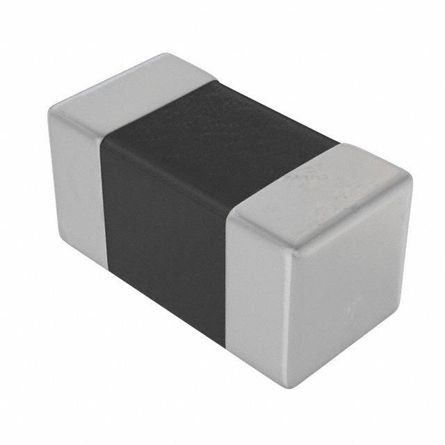
Taiyo Yuden(太阳诱电)GMK212SD223JG-T是一款多层陶瓷电容器(MLCC),容量22 nF(223表示22×10³ pF),额定电压25 V,X7R温度特性,±5%容差,0805封装(2.0×1.25 mm)。其典型应用场景包括:
- 电源去耦与旁路:广泛用于IC(如MCU、FPGA、DC-DC转换器)的VDD/VSS引脚附近,滤除高频噪声(数十MHz至数百MHz),保障供电稳定性;
- 信号线滤波:在USB、HDMI、LVDS等高速接口的端接或ESD保护电路中,配合TVS器件抑制高频干扰;
- 模拟电路退耦:应用于运算放大器、ADC/DAC参考电源端,提升信噪比与精度;
- 消费电子与工业设备:常见于智能手机主板、智能穿戴设备、路由器、PLC模块等对尺寸、可靠性及温漂要求较高的紧凑型电子产品中。
该型号具备优异的抗弯裂设计(Soft Termination结构)、低ESL/ESR及AEC-Q200兼容性(部分批次),适用于自动化贴装及回流焊工艺,适合高可靠性、小体积、宽温(−55℃~+125℃)运行环境。
| 参数 | 数值 |
| 产品目录 | |
| 描述 | CAP CER 0.022UF 35V 5% 0805 |
| 产品分类 | |
| 品牌 | Taiyo Yuden |
| 数据手册 | |
| 产品图片 |
|
| 产品型号 | GMK212SD223JG-T |
| rohs | 无铅 / 符合限制有害物质指令(RoHS)规范要求 |
| 产品系列 | CFCAP™ |
| 产品目录绘图 |
|
| 产品目录页面 | |
| 其它名称 | 587-1121-2 |
| 包装 | 带卷 (TR) |
| 厚度(最大值) | 0.053"(1.35mm) |
| 大小/尺寸 | 0.079" 长 x 0.049" 宽(2.00mm x 1.25mm) |
| 安装类型 | 表面贴装,MLCC |
| 容差 | ±5% |
| 封装/外壳 | 0805(2012 公制) |
| 工作温度 | -55°C ~ 125°C |
| 应用 | RF,微波,高频 |
| 引线形式 | - |
| 引线间距 | - |
| 标准包装 | 3,000 |
| 温度系数 | - |
| 特性 | 低失真 |
| 电压-额定 | 35V |
| 电容 | 0.022µF |
| 等级 | - |
| 高度-安装(最大值) | - |


- 商务部:美国ITC正式对集成电路等产品启动337调查
- 曝三星4nm工艺存在良率问题 高通将骁龙8 Gen1或转产台积电
- 太阳诱电将投资9.5亿元在常州建新厂生产MLCC 预计2023年完工
- 英特尔发布欧洲新工厂建设计划 深化IDM 2.0 战略
- 台积电先进制程称霸业界 有大客户加持明年业绩稳了
- 达到5530亿美元!SIA预计今年全球半导体销售额将创下新高
- 英特尔拟将自动驾驶子公司Mobileye上市 估值或超500亿美元
- 三星加码芯片和SET,合并消费电子和移动部门,撤换高东真等 CEO
- 三星电子宣布重大人事变动 还合并消费电子和移动部门
- 海关总署:前11个月进口集成电路产品价值2.52万亿元 增长14.8%

.jpg)


PDF Datasheet 数据手册内容提取
Notice for TAIYO YUDEN products Please read this notice before using the TAIYO YUDEN products. REMINDERS ■ Product Information in this Catalog (4) Power generation control equipment (nuclear power, Product information in this catalog is as of October 2019. All of the hydroelectric power, thermal power plant control system, etc.) contents specified herein and production status of the products listed (5) Undersea equipment (submarine repeating equipment, in this catalog are subject to change without notice due to technical underwater work equipment, etc.) improvement of our products, etc. Therefore, please check for the (6) Military equipment latest information carefully before practical application or use of our (7) Any other equipment requiring extremely high levels of safety products. and/or reliability equal to the equipment listed above Please note that TAIYO YUDEN shall not be in any way responsible *Notes: for any damages and defects in products or equipment incorporating 1. There is a possibility that our products can be used only our products, which are caused under the conditions other than those for aviation equipment that does not directly affect the safe specified in this catalog or individual product specification sheets. operation of aircraft (e.g., in-flight entertainment, cabin light, electric seat, cooking equipment) if such use meets ■ Approval of Product Specifications requirements specified separately by TAIYO YUDEN. Please Please contact TAIYO YUDEN for further details of product be sure to contact TAIYO YUDEN for further information specifications as the individual product specification sheets are before using our products for such aviation equipment. available. When using our products, please be sure to approve our 2. Implantable medical devices contain not only internal unit product specifications or make a written agreement on the product which is implanted in a body, but also external unit which is specification with TAIYO YUDEN in advance. connected to the internal unit. ■ Pre-Evaluation in the Actual Equipment and Conditions 4. Limitation of Liability Please conduct validation and verification of our products in actual Please note that unless you obtain prior written consent of TAIYO conditions of mounting and operating environment before using our YUDEN, TAIYO YUDEN shall not be in any way responsible for products. any damages incurred by you or third parties arising from use of the products listed in this catalog for any equipment that is not ■ Limited Application intended for use by TAIYO YUDEN, or any equipment requiring 1. Equipment Intended for Use inquiry to TAIYO YUDEN or prohibited for use by TAIYO YUDEN The products listed in this catalog are intended for general- as described above. purpose and standard use in general electronic equipment (e.g., AV equipment, OA equipment, home electric appliances, office ■ Safety Design equipment, information and communication equipment including, When using our products for high safety and/or reliability-required without limitation, mobile phone, and PC) and other equipment equipment or circuits, please fully perform safety and/or reliability specified in this catalog or the individual product specification sheets. evaluation. In addition, please install (i) systems equipped with a protection circuit and a protection device and/or (ii) systems TAIYO YUDEN has the line-up of the products intended for equipped with a redundant circuit or other system to prevent an use in automotive electronic equipment, telecommunications unsafe status in the event of a single fault for a failsafe design to infrastructure and industrial equipment, or medical devices ensure safety. classified as GHTF Classes A to C (Japan Classes I to III). Therefore, when using our products for these equipment, ■ Intellectual Property Rights please check available applications specified in this catalog Information contained in this catalog is intended to convey examples or the individual product specification sheets and use the of typical performances and/or applications of our products and is corresponding products. not intended to make any warranty with respect to the intellectual property rights or any other related rights of TAIYO YUDEN or any 2. Equipment Requiring Inquiry third parties nor grant any license under such rights. Please be sure to contact TAIYO YUDEN for further information before using the products listed in this catalog for the following ■ Limited Warranty equipment (excluding intended equipment as specified in this Please note that the scope of warranty for our products is limited to catalog or the individual product specification sheets) which may the delivered our products themselves and TAIYO YUDEN shall not cause loss of human life, bodily injury, serious property damage be in any way responsible for any damages resulting from a failure and/or serious public impact due to a failure or defect of the or defect in our products. Notwithstanding the foregoing, if there is products and/or malfunction attributed thereto. a written agreement (e.g., supply and purchase agreement, quality (1) Transportation equipment (automotive powertrain control assurance agreement) signed by TAIYO YUDEN and your company, system, train control system, and ship control system, etc.) TAIYO YUDEN will warrant our products in accordance with such (2) Traffic signal equipment agreement. (3) Disaster prevention equipment, crime prevention equipment (4) Medical devices classified as GHTF Class C (Japan Class III) ■ TAIYO YUDEN’s Official Sales Channel (5) Highly public information network equipment, data- The contents of this catalog are applicable to our products which are processing equipment (telephone exchange, and base purchased from our sales offices or authorized distributors (hereinafter station, etc.) “TAIYO YUDEN’s official sales channel”). Please note that the contents (6) Any other equipment requiring high levels of quality and/or of this catalog are not applicable to our products purchased from any reliability equal to the equipment listed above seller other than TAIYO YUDEN’s official sales channel. 3. Equipment Prohibited for Use ■ Caution for Export Please do not incorporate our products into the following Some of our products listed in this catalog may require specific equipment requiring extremely high levels of safety and/or procedures for export according to“ U.S. Export Administration reliability. Regulations”,“ Foreign Exchange and Foreign Trade Control Law” (1) Aerospace equipment (artificial satellite, rocket, etc.) of Japan, and other applicable regulations. Should you have any (2) Aviation equipment *1 questions on this matter, please contact our sales staff. (3) Medical devices classified as GHTF Class D (Japan Class IV), implantable medical devices *2 20
for General Electronic Equipment for General Electronic Equipment MULTILAYER CERAMIC CAPACITORS MULTILAYER CERAMIC CAPACITORS C WAVE REFLOW AC PAER WAVE REFLOW CA ■PARTS NUMBER ITM OIC RS J M K 3 1 6 △ B J 1 0 6 M L - T △ △=Blank space ① ② ③ ④ ⑤ ⑥ ⑦ ⑧ ⑨ ⑩ ⑪ ⑫ M ①Rated voltage ③End termination U Code Rated voltage[VDC] Code End termination L T P 2.5 K Plated ILA A 4 S Cu Internal Electrodes (For High Frequency) Y J 6.3 E R L 10 ④Dimension(L×W) C E 16 Type Dimensions EIA(inch) E T 25 (L×W)[mm] R A G 35 021 0.25× 0.125 008004 M U 50 042 0.4 × 0.2 01005 IC H 100 063 0.6 × 0.3 0201 Q 250 1.0 × 0.5 0402 C 105 A S 630 0.52× 1.0 ※ 0204 P X 2000 1.6 × 0.8 0603 A 107 C 0.8 × 1.6 ※ 0306 IT ②Series name 212 2.0 × 1.25 0805 O Code Series name 1.25× 2.0 ※ 0508 R M Multilayer ceramic capacitor 316 3.2 × 1.6 1206 S V Multilayer ceramic capacitor for high frequency 325 3.2 × 2.5 1210 W LW reverse type multilayer capacitor 432 4.5 × 3.2 1812 Note : ※LW reverse type(□WK) only ⑤Dimension tolerance Code Type L[mm] W[mm] T[mm] △ ALL Standard Standard Standard 063 0.6±0.05 0.3±0.05 0.3±0.05 105 1.0±0.10 0.5±0.10 0.5±0.10 107 1.6+0.15/-0.05 0.8+0.15/-0.05 0.8+0.15/-0.05 0.45±0.05 A 212 2.0+0.15/-0.05 1.25+0.15/-0.05 0.85±0.10 1.25+0.15/-0.05 0.85±0.10 316 3.2±0.20 1.6±0.20 1.6±0.20 325 3.2±0.30 2.5±0.30 2.5±0.30 063 0.6±0.09 0.3±0.09 0.3±0.09 105 1.0+0.15/-0.05 0.5+0.15/-0.05 0.5+0.15/-0.05 0.45±0.05 107 1.6+0.20/-0 0.8+0.20/-0 0.8+0.20/-0 B 0.45±0.05 212 2.0+0.20/-0 1.25+0.20/-0 0.85±0.10 1.25+0.20/-0 316 3.2±0.30 1.6±0.30 1.6±0.30 C 105 1.0+0.20/-0 0.5+0.20/-0 0.5+0.20/-0 063 0.6 + 0.25/- 0 0.3 + 0.25/- 0 0.3 + 0.25/ - 0 E 105 1.0+0.30/-0 0.5+0.30/-0 0.5+0.30/-0 Note: cf. STANDARD EXTERNAL DIMENSIONS △= Blank space ⑥Temperature characteristics code ■High dielectric type(Excluding Super low distortion multilayer ceramic capacitor) Applicable Temperature Capacitance Tolerance Code Ref. Temp.[℃] Capacitance change standard range[℃] tolerance code ±10% K JIS B -25~+ 85 20 ±10% ±20% M BJ ±10% K EIA X5R -55~+ 85 25 ±15% ±20% M ±10% K B7 EIA X7R -55~+125 25 ±15% ±20% M ±10% K C6 EIA X6S -55~+105 25 ±22% ±20% M ±10% K C7 EIA X7S -55~+125 25 ±22% ±20% M ±10% K LD(※) EIA X5R -55~+ 85 25 ±15% ±20% M Note : ※.LD Low distortion high value multilayer ceramic capacitor △= Blank space c_mlcc_e-E08R01 ▶ This catalog contains the typical specification only due to the limitation of space. When you consider the purchase of our products, please check our product specification sheets. For details of each product (characteristics graph, reliability information, precautions for use, and so on), see our website (http://www.ty-top.com/) . 12 20
for General Electronic Equipment ■Temperature compensating type Applicable Temperature Capacitance Tolerance Code Ref. Temp.[℃] Capacitance change standard range[℃] tolerance code C ±0.05pF A AC ±0.1pF B PAER CA CG EIA C0G -55~+125 25 0±30ppm/℃ ±0.25pF C ITM ±0.5pF D ORSIC ±5% J ±0.25pF C JIS UJ 20 UJ -55~+125 -750±120ppm/℃ ±0.5pF D M EIA U2J 25 ±5% J U JIS UK -55~+125 20 L UK -750±250ppm/℃ ±0.25pF C T EIA U2K -55~+125 25 IL A Y ⑥Series code ⑨Thickness E R ・Super low distortion multilayer ceramic capacitor Code Thickness[mm] C Code Series code K 0.125 E SD Standard H 0.13 R A E 0.18 M ・Medium-High Voltage Multilayer Ceramic Capacitor C 0.2 IC Code Series code D C SD Standard P A T 0.3 PA ⑦Nominal capacitance K 0.45(107type or more) C Code V IT Nominal capacitance 0.5 O (example) W R 0R5 0.5pF A 0.8 S 010 1pF D 0.85(212type or more) 100 10pF F 1.15 101 100pF G 1.25 102 1,000pF L 1.6 103 10,000pF N 1.9 104 0.1μF Y 2.0 max 105 1.0μF M 2.5 106 10μF 107 100μF ⑩Special code Note : R=Decimal point Code Special code - Standard ⑧Capacitance tolerance Code Capacitance tolerance ⑪Packaging A ±0.05pF Code Packaging B ±0.1pF F φ178mm Taping (2mm pitch) C ±0.25pF T φ178mm Taping (4mm pitch) D ±0.5pF φ178mm Taping (4mm pitch, 1000 pcs/reel) P F ±1pF 325 type(Thickness code M) G ±2% φ178mm Taping (2mm pitch)105type only R J ±5% (Thickness code E,H) K ±10% W φ178mm Taping(1mm pitch)021/042type only M ±20% Z +80/-20% ⑫Internal code Code Internal code △ Standard ▶ This catalog contains the typical specification only due to the limitation of space. When you consider the purchase of our products, please check our product specification sheets. For details of each product (characteristics graph, reliability information, precautions for use, and so on), see our website (http://www.ty-top.com/) . c_mlcc_e-E08R01 20 13
for General Electronic Equipment ■STANDARD EXTERNAL DIMENSIONS W Dimension [mm] Type( EIA ) L L W T *1 e C □MK021(008004) 0.25±0.013 0.125±0.013 0.125±0.013 K 0.0675±0.0275 AC PAER T □VS021(008004) 0.25±0.013 0.125±0.013 0.125±0.013 K 0.0675±0.0275 CA C ITM □MK042(01005) 0.4±0.02 0.2±0.02 0.2±0.02 0.1±0.03 OIC e D RS □VS042(01005) 0.4±0.02 0.2±0.02 0.2±0.02 C 0.1±0.03 P □MK063(0201) 0.6±0.03 0.3±0.03 0.3±0.03 0.15±0.05 T M 0.13±0.02 H L U 0.18±0.02 E LT □MK105(0402) 1.0±0.05 0.5±0.05 0.2±0.02 C 0.25±0.10 IL W 0.3±0.03 P A 0.5±0.05 V Y E □VK105(0402) 1.0±0.05 0.5±0.05 0.5±0.05 W 0.25±0.10 R □WK105(0204)※ 0.52±0.05 1.0±0.05 0.3±0.05 P 0.18±0.08 CE T □MK107(0603) 1.6±0.10 0.8±0.10 0.45±0.05 K 0.35±0.25 R 0.8±0.10 A A e □WK107(0306)※ 0.8±0.10 1.6±0.10 0.5±0.05 V 0.25±0.15 M 0.45±0.05 K IC □MK212(0805) 2.0±0.10 1.25±0.10 0.85±0.10 D 0.5±0.25 C ※ LW reverse type 1.25±0.10 G A □WK212(0508)※ 1.25±0.15 2.0±0.15 0.85±0.10 D 0.3±0.2 P A 0.85±0.10 D C □MK316(1206) 3.2±0.15 1.6±0.15 1.15±0.10 F 0.5+0.35/-0.25 IT 1.6±0.20 L O 0.85±0.10 D R S 1.15±0.10 F □MK325(1210) 3.2±0.30 2.5±0.20 1.9±0.20 N 0.6±0.3 1.9+0.1/-0.2 Y 2.5±0.20 M 2.0+0/-0.30 Y 0.6±0.4 □MK432(1812) 4.5±0.40 3.2±0.30 2.5±0.20 M 0.9±0.6 Note : ※. LW reverse type, *1.Thickness code ■STANDARD QUANTITY Dimension Standard quantity[pcs] Type EIA(inch) [mm] Code Paper tape Embossed tape 021 008004 0.125 K - 50000 C 042 01005 0.2 - 40000 D P 063 0201 0.3 15000 - T 0.13 H - 20000 0.18 E - 15000 0.2 C 20000 - 0402 105 0.3 P 15000 - V 0.5 W 10000 - 0204 ※ 0.30 P 0.45 K 0603 4000 - 107 0.8 A 0306 ※ 0.50 V - 4000 0.45 K 4000 - 0805 0.85 D 212 1.25 G - 3000 0508 ※ 0.85 D 4000 - 0.85 D 4000 - 316 1206 1.15 F - 3000 1.6 L - 2000 0.85 D 1.15 F - 2000 325 1210 1.9 N 2.0 max Y 2.5 M - 1000 2.0 max Y - 1000 432 1812 2.5 M - 500 Note : ※.LW Reverse type(□WK) c_mlcc_e-E08R01 ▶ This catalog contains the typical specification only due to the limitation of space. When you consider the purchase of our products, please check our product specification sheets. For details of each product (characteristics graph, reliability information, precautions for use, and so on), see our website (http://www.ty-top.com/) . 14 20
for General Electronic Equipment ■PARTS NUMBER Multilayer Ceramic Capacitors(Temperature compensating type) ●021TYPE C 【Temperature Characteristic CG : CG/C0G(-55~+125℃)】 0.125mm thickness(K) AC Part number 1 Part number 2 Rated[ Vv]oltage cThaermapceteraritsutrices Capa c[Fit]ance Capacitance tolerance (at m1QMinHz) Rated vHoTltLaTge x %Thickness*3 [mm] SRWo:R:lWdeeafrlvoinewg PACITERAM TMK021 CG010[]K-W CG C0G 1p ±0.1pF, ±0.25pF 420 200 0.125±0.013 R OIC TMK021 CG1R1[]K-W CG C0G 1.1p ±0.1pF, ±0.25pF 422 200 0.125±0.013 R RS TMK021 CG1R2[]K-W CG C0G 1.2p ±0.1pF, ±0.25pF 424 200 0.125±0.013 R TMK021 CG1R3[]K-W CG C0G 1.3p ±0.1pF, ±0.25pF 426 200 0.125±0.013 R TMK021 CG1R4[]K-W CG C0G 1.4p ±0.1pF, ±0.25pF 428 200 0.125±0.013 R TMK021 CG1R5[]K-W CG C0G 1.5p ±0.1pF, ±0.25pF 430 200 0.125±0.013 R M TMK021 CG1R6[]K-W CG C0G 1.6p ±0.1pF, ±0.25pF 432 200 0.125±0.013 R U TMK021 CG1R7[]K-W CG C0G 1.7p ±0.1pF, ±0.25pF 434 200 0.125±0.013 R L TMK021 CG1R8[]K-W CG C0G 1.8p ±0.1pF, ±0.25pF 436 200 0.125±0.013 R T TMK021 CG1R9[]K-W CG C0G 1.9p ±0.1pF, ±0.25pF 438 200 0.125±0.013 R IL TMK021 CG020[]K-W CG C0G 2p ±0.1pF, ±0.25pF 440 200 0.125±0.013 R A TMK021 CG2R1[]K-W CG C0G 2.1p ±0.1pF, ±0.25pF 442 200 0.125±0.013 R Y TMK021 CG2R2[]K-W CG C0G 2.2p ±0.1pF, ±0.25pF 444 200 0.125±0.013 R E R TMK021 CG2R3[]K-W CG C0G 2.3p ±0.1pF, ±0.25pF 446 200 0.125±0.013 R TMK021 CG2R4[]K-W CG C0G 2.4p ±0.1pF, ±0.25pF 448 200 0.125±0.013 R C TMK021 CG2R5[]K-W CG C0G 2.5p ±0.1pF, ±0.25pF 450 200 0.125±0.013 R E R TMK021 CG2R6[]K-W CG C0G 2.6p ±0.1pF, ±0.25pF 452 200 0.125±0.013 R A TMK021 CG2R7[]K-W CG C0G 2.7p ±0.1pF, ±0.25pF 454 200 0.125±0.013 R M TMK021 CG2R8[]K-W CG C0G 2.8p ±0.1pF, ±0.25pF 456 200 0.125±0.013 R TMK021 CG2R9[]K-W CG C0G 2.9p ±0.1pF, ±0.25pF 458 200 0.125±0.013 R IC TMK021 CG030[]K-W CG C0G 3p ±0.1pF, ±0.25pF 460 200 0.125±0.013 R TMK021 CG3R1[]K-W CG C0G 3.1p ±0.1pF, ±0.25pF 462 200 0.125±0.013 R C TMK021 CG3R2[]K-W CG C0G 3.2p ±0.1pF, ±0.25pF 464 200 0.125±0.013 R A TMK021 CG3R3[]K-W CG C0G 3.3p ±0.1pF, ±0.25pF 466 200 0.125±0.013 R P A TMK021 CG3R4[]K-W CG C0G 3.4p ±0.1pF, ±0.25pF 468 200 0.125±0.013 R C TTMMKK002211 CCGG33RR56[[]]KK--WW CCGG CC00GG 33..56pp ±±00..11ppFF,, ±±00..2255ppFF 447702 220000 00..112255±±00..001133 RR IT TMK021 CG3R7[]K-W CG C0G 3.7p ±0.1pF, ±0.25pF 474 200 0.125±0.013 R O TMK021 CG3R8[]K-W CG C0G 3.8p ±0.1pF, ±0.25pF 476 200 0.125±0.013 R R TMK021 CG3R9[]K-W CG C0G 3.9p ±0.1pF, ±0.25pF 478 200 0.125±0.013 R S TMK021 CG040[]K-W CG C0G 4p ±0.1pF, ±0.25pF 480 200 0.125±0.013 R TMK021 CG4R1[]K-W CG C0G 4.1p ±0.1pF, ±0.25pF 482 200 0.125±0.013 R TMK021 CG4R2[]K-W CG C0G 4.2p ±0.1pF, ±0.25pF 484 200 0.125±0.013 R TMK021 CG4R3[]K-W CG C0G 4.3p ±0.1pF, ±0.25pF 486 200 0.125±0.013 R TMK021 CG4R4[]K-W CG C0G 4.4p ±0.1pF, ±0.25pF 488 200 0.125±0.013 R TMK021 CG4R5[]K-W CG C0G 4.5p ±0.1pF, ±0.25pF 490 200 0.125±0.013 R TMK021 CG4R6[]K-W CG C0G 4.6p ±0.1pF, ±0.25pF 492 200 0.125±0.013 R TMK021 CG4R7[]K-W CG C0G 4.7p ±0.1pF, ±0.25pF 494 200 0.125±0.013 R TMK021 CG4R8[]K-W CG C0G 4.8p ±0.1pF, ±0.25pF 496 200 0.125±0.013 R TMK021 CG4R9[]K-W CG C0G 4.9p ±0.1pF, ±0.25pF 498 200 0.125±0.013 R TMK021 CG050[]K-W CG C0G 5p ±0.1pF, ±0.25pF 500 200 0.125±0.013 R TMK021 CG5R1[]K-W CG C0G 5.1p ±0.25pF, ±0.5pF 502 200 0.125±0.013 R TMK021 CG5R2[]K-W 25 CG C0G 5.2p ±0.25pF, ±0.5pF 504 200 0.125±0.013 R TMK021 CG5R3[]K-W CG C0G 5.3p ±0.25pF, ±0.5pF 506 200 0.125±0.013 R TMK021 CG5R4[]K-W CG C0G 5.4p ±0.25pF, ±0.5pF 508 200 0.125±0.013 R TMK021 CG5R5[]K-W CG C0G 5.5p ±0.25pF, ±0.5pF 510 200 0.125±0.013 R TMK021 CG5R6[]K-W CG C0G 5.6p ±0.25pF, ±0.5pF 512 200 0.125±0.013 R TMK021 CG5R7[]K-W CG C0G 5.7p ±0.25pF, ±0.5pF 514 200 0.125±0.013 R TMK021 CG5R8[]K-W CG C0G 5.8p ±0.25pF, ±0.5pF 516 200 0.125±0.013 R TMK021 CG5R9[]K-W CG C0G 5.9p ±0.25pF, ±0.5pF 518 200 0.125±0.013 R TMK021 CG060[]K-W CG C0G 6p ±0.25pF, ±0.5pF 520 200 0.125±0.013 R TMK021 CG6R1[]K-W CG C0G 6.1p ±0.25pF, ±0.5pF 522 200 0.125±0.013 R TMK021 CG6R2[]K-W CG C0G 6.2p ±0.25pF, ±0.5pF 524 200 0.125±0.013 R TMK021 CG6R3[]K-W CG C0G 6.3p ±0.25pF, ±0.5pF 526 200 0.125±0.013 R TMK021 CG6R4[]K-W CG C0G 6.4p ±0.25pF, ±0.5pF 528 200 0.125±0.013 R TMK021 CG6R5[]K-W CG C0G 6.5p ±0.25pF, ±0.5pF 530 200 0.125±0.013 R TMK021 CG6R6[]K-W CG C0G 6.6p ±0.25pF, ±0.5pF 532 200 0.125±0.013 R TMK021 CG6R7[]K-W CG C0G 6.7p ±0.25pF, ±0.5pF 534 200 0.125±0.013 R TMK021 CG6R8[]K-W CG C0G 6.8p ±0.25pF, ±0.5pF 536 200 0.125±0.013 R TMK021 CG6R9[]K-W CG C0G 6.9p ±0.25pF, ±0.5pF 538 200 0.125±0.013 R TMK021 CG070[]K-W CG C0G 7p ±0.25pF, ±0.5pF 540 200 0.125±0.013 R TMK021 CG7R1[]K-W CG C0G 7.1p ±0.25pF, ±0.5pF 542 200 0.125±0.013 R TMK021 CG7R2[]K-W CG C0G 7.2p ±0.25pF, ±0.5pF 544 200 0.125±0.013 R TMK021 CG7R3[]K-W CG C0G 7.3p ±0.25pF, ±0.5pF 546 200 0.125±0.013 R TMK021 CG7R4[]K-W CG C0G 7.4p ±0.25pF, ±0.5pF 548 200 0.125±0.013 R TMK021 CG7R5[]K-W CG C0G 7.5p ±0.25pF, ±0.5pF 550 200 0.125±0.013 R TMK021 CG7R6[]K-W CG C0G 7.6p ±0.25pF, ±0.5pF 552 200 0.125±0.013 R TMK021 CG7R7[]K-W CG C0G 7.7p ±0.25pF, ±0.5pF 554 200 0.125±0.013 R TMK021 CG7R8[]K-W CG C0G 7.8p ±0.25pF, ±0.5pF 556 200 0.125±0.013 R TMK021 CG7R9[]K-W CG C0G 7.9p ±0.25pF, ±0.5pF 558 200 0.125±0.013 R TMK021 CG080[]K-W CG C0G 8p ±0.25pF, ±0.5pF 560 200 0.125±0.013 R TMK021 CG8R1[]K-W CG C0G 8.1p ±0.25pF, ±0.5pF 562 200 0.125±0.013 R TMK021 CG8R2[]K-W CG C0G 8.2p ±0.25pF, ±0.5pF 564 200 0.125±0.013 R TMK021 CG8R3[]K-W CG C0G 8.3p ±0.25pF, ±0.5pF 566 200 0.125±0.013 R TMK021 CG8R4[]K-W CG C0G 8.4p ±0.25pF, ±0.5pF 568 200 0.125±0.013 R TMK021 CG8R5[]K-W CG C0G 8.5p ±0.25pF, ±0.5pF 570 200 0.125±0.013 R TMK021 CG8R6[]K-W CG C0G 8.6p ±0.25pF, ±0.5pF 572 200 0.125±0.013 R TMK021 CG8R7[]K-W CG C0G 8.7p ±0.25pF, ±0.5pF 574 200 0.125±0.013 R TMK021 CG8R8[]K-W CG C0G 8.8p ±0.25pF, ±0.5pF 576 200 0.125±0.013 R TMK021 CG8R9[]K-W CG C0G 8.9p ±0.25pF, ±0.5pF 578 200 0.125±0.013 R TMK021 CG090[]K-W CG C0G 9p ±0.25pF, ±0.5pF 580 200 0.125±0.013 R TMK021 CG9R1[]K-W CG C0G 9.1p ±0.25pF, ±0.5pF 582 200 0.125±0.013 R TMK021 CG9R2[]K-W CG C0G 9.2p ±0.25pF, ±0.5pF 584 200 0.125±0.013 R TMK021 CG9R3[]K-W CG C0G 9.3p ±0.25pF, ±0.5pF 586 200 0.125±0.013 R TMK021 CG9R4[]K-W CG C0G 9.4p ±0.25pF, ±0.5pF 588 200 0.125±0.013 R c_mlcc_e-E08R01 ▶ This catalog contains the typical specification only due to the limitation of space. When you consider the purchase of our products, please check our product specification sheets. For details of each product (characteristics graph, reliability information, precautions for use, and so on), see our website (http://www.ty-top.com/) . 20 23
for General Electronic Equipment ■PARTS NUMBER Part number 1 Part number 2 Rated[ Vv]oltage cThaermapceteraritsutrices Capa c[Fit]ance Capacitance tolerance (at m1QMinHz) Rated vHoTltLaTge x %Thickness*3 [mm] SRWo:R:lWdeeafrlvoinewg C TMK021 CG9R5[]K-W CG C0G 9.5p ±0.25pF, ±0.5pF 590 200 0.125±0.013 R AC TMK021 CG9R6[]K-W CG C0G 9.6p ±0.25pF, ±0.5pF 592 200 0.125±0.013 R PAER TMK021 CG9R7[]K-W CG C0G 9.7p ±0.25pF, ±0.5pF 594 200 0.125±0.013 R CA TMK021 CG9R8[]K-W CG C0G 9.8p ±0.25pF, ±0.5pF 596 200 0.125±0.013 R ITM TMK021 CG9R9[]K-W CG C0G 9.9p ±0.25pF, ±0.5pF 598 200 0.125±0.013 R OIC TMK021 CG100DK-W 25 CG C0G 10p ±0.5pF 600 200 0.125±0.013 R RS TMK021 CG120JK-W CG C0G 12p ±5% 640 200 0.125±0.013 R TMK021 CG150JK-W CG C0G 15p ±5% 700 200 0.125±0.013 R TMK021 CG180JK-W CG C0G 18p ±5% 760 200 0.125±0.013 R TMK021 CG220JK-W CG C0G 22p ±5% 840 200 0.125±0.013 R M TMK021 CG270JK-W CG C0G 27p ±5% 940 200 0.125±0.013 R U EMK021 CG330JK-W CG C0G 33p ±5% 1000 150 0.125±0.013 R LT EEMMKK002211 CCGG349700JJKK--WW 16 CCGG CC00GG 3497pp ±±55%% 11000000 115500 00..112255±±00..001133 RR IL EMK021 CG560JK-W CG C0G 56p ±5% 1000 150 0.125±0.013 R A LMK021 CG680JK-W CG C0G 68p ±5% 1000 200 0.125±0.013 R Y LMK021 CG820JK-W 10 CG C0G 82p ±5% 1000 200 0.125±0.013 R E R LMK021 CG101JK-W CG C0G 100p ±5% 1000 200 0.125±0.013 R C E R ●042TYPE A 【Temperature Characteristic CG : CG/C0G(-55~+125℃)】 0.2mm thickness(C,D) MIC Part number 1 Part number 2 Rated[ Vv]oltage cThaermapceteraritsutrices Capa c[Fit]ance Capacitance tolerance (at m1QMinHz) Rated vHoTltLaTge x %Thickness*3 [mm] SRWo:R:lWdeeafrlvoinewg C TMK042 CG010[]D-W CG C0G 1p ±0.05pF, ±0.1pF, ±0.25pF 420 200 0.2±0.02 R A TMK042 CG1R1[]D-W CG C0G 1.1p ±0.05pF, ±0.1pF, ±0.25pF 422 200 0.2±0.02 R P TMK042 CG1R2[]D-W CG C0G 1.2p ±0.05pF, ±0.1pF, ±0.25pF 424 200 0.2±0.02 R A TMK042 CG1R3[]D-W CG C0G 1.3p ±0.05pF, ±0.1pF, ±0.25pF 426 200 0.2±0.02 R C TMK042 CG1R4[]D-W CG C0G 1.4p ±0.05pF, ±0.1pF, ±0.25pF 428 200 0.2±0.02 R IT TMK042 CG1R5[]D-W CG C0G 1.5p ±0.05pF, ±0.1pF, ±0.25pF 430 200 0.2±0.02 R O TMK042 CG1R6[]D-W CG C0G 1.6p ±0.05pF, ±0.1pF, ±0.25pF 432 200 0.2±0.02 R TMK042 CG1R7[]D-W CG C0G 1.7p ±0.05pF, ±0.1pF, ±0.25pF 434 200 0.2±0.02 R R S TMK042 CG1R8[]D-W CG C0G 1.8p ±0.05pF, ±0.1pF, ±0.25pF 436 200 0.2±0.02 R TMK042 CG1R9[]D-W CG C0G 1.9p ±0.05pF, ±0.1pF, ±0.25pF 438 200 0.2±0.02 R TMK042 CG020[]D-W CG C0G 2p ±0.05pF, ±0.1pF, ±0.25pF 440 200 0.2±0.02 R TMK042 CG2R1[]D-W CG C0G 2.1p ±0.05pF, ±0.1pF, ±0.25pF 442 200 0.2±0.02 R TMK042 CG2R2[]D-W CG C0G 2.2p ±0.05pF, ±0.1pF, ±0.25pF 444 200 0.2±0.02 R TMK042 CG2R3[]D-W CG C0G 2.3p ±0.05pF, ±0.1pF, ±0.25pF 446 200 0.2±0.02 R TMK042 CG2R4[]D-W CG C0G 2.4p ±0.05pF, ±0.1pF, ±0.25pF 448 200 0.2±0.02 R TMK042 CG2R5[]D-W CG C0G 2.5p ±0.05pF, ±0.1pF, ±0.25pF 450 200 0.2±0.02 R TMK042 CG2R6[]D-W CG C0G 2.6p ±0.05pF, ±0.1pF, ±0.25pF 452 200 0.2±0.02 R TMK042 CG2R7[]D-W CG C0G 2.7p ±0.05pF, ±0.1pF, ±0.25pF 454 200 0.2±0.02 R TMK042 CG2R8[]D-W CG C0G 2.8p ±0.05pF, ±0.1pF, ±0.25pF 456 200 0.2±0.02 R TMK042 CG2R9[]D-W CG C0G 2.9p ±0.05pF, ±0.1pF, ±0.25pF 458 200 0.2±0.02 R TMK042 CG030[]D-W CG C0G 3p ±0.05pF, ±0.1pF, ±0.25pF 460 200 0.2±0.02 R TMK042 CG3R1[]D-W CG C0G 3.1p ±0.1pF, ±0.25pF 462 200 0.2±0.02 R TMK042 CG3R2[]D-W CG C0G 3.2p ±0.1pF, ±0.25pF 464 200 0.2±0.02 R TMK042 CG3R3[]D-W CG C0G 3.3p ±0.1pF, ±0.25pF 466 200 0.2±0.02 R TMK042 CG3R4[]D-W CG C0G 3.4p ±0.1pF, ±0.25pF 468 200 0.2±0.02 R TMK042 CG3R5[]D-W CG C0G 3.5p ±0.1pF, ±0.25pF 470 200 0.2±0.02 R TMK042 CG3R6[]D-W CG C0G 3.6p ±0.1pF, ±0.25pF 472 200 0.2±0.02 R TMK042 CG3R7[]D-W CG C0G 3.7p ±0.1pF, ±0.25pF 474 200 0.2±0.02 R TMK042 CG3R8[]D-W CG C0G 3.8p ±0.1pF, ±0.25pF 476 200 0.2±0.02 R TMK042 CG3R9[]D-W CG C0G 3.9p ±0.1pF, ±0.25pF 478 200 0.2±0.02 R TMK042 CG040[]D-W CG C0G 4p ±0.1pF, ±0.25pF 480 200 0.2±0.02 R TMK042 CG4R1[]D-W CG C0G 4.1p ±0.1pF, ±0.25pF 482 200 0.2±0.02 R 25 TMK042 CG4R2[]D-W CG C0G 4.2p ±0.1pF, ±0.25pF 484 200 0.2±0.02 R TMK042 CG4R3[]D-W CG C0G 4.3p ±0.1pF, ±0.25pF 486 200 0.2±0.02 R TMK042 CG4R4[]D-W CG C0G 4.4p ±0.1pF, ±0.25pF 488 200 0.2±0.02 R TMK042 CG4R5[]D-W CG C0G 4.5p ±0.1pF, ±0.25pF 490 200 0.2±0.02 R TMK042 CG4R6[]D-W CG C0G 4.6p ±0.1pF, ±0.25pF 492 200 0.2±0.02 R TMK042 CG4R7[]D-W CG C0G 4.7p ±0.1pF, ±0.25pF 494 200 0.2±0.02 R TMK042 CG4R8[]D-W CG C0G 4.8p ±0.1pF, ±0.25pF 496 200 0.2±0.02 R TMK042 CG4R9[]D-W CG C0G 4.9p ±0.1pF, ±0.25pF 498 200 0.2±0.02 R TMK042 CG050[]D-W CG C0G 5p ±0.1pF, ±0.25pF 500 200 0.2±0.02 R TMK042 CG5R1[]D-W CG C0G 5.1p ±0.1pF, ±0.25pF, ±0.5pF 502 200 0.2±0.02 R TMK042 CG5R2[]D-W CG C0G 5.2p ±0.1pF, ±0.25pF, ±0.5pF 504 200 0.2±0.02 R TMK042 CG5R3[]D-W CG C0G 5.3p ±0.1pF, ±0.25pF, ±0.5pF 506 200 0.2±0.02 R TMK042 CG5R4[]D-W CG C0G 5.4p ±0.1pF, ±0.25pF, ±0.5pF 508 200 0.2±0.02 R TMK042 CG5R5[]D-W CG C0G 5.5p ±0.1pF, ±0.25pF, ±0.5pF 510 200 0.2±0.02 R TMK042 CG5R6[]D-W CG C0G 5.6p ±0.1pF, ±0.25pF, ±0.5pF 512 200 0.2±0.02 R TMK042 CG5R7[]D-W CG C0G 5.7p ±0.1pF, ±0.25pF, ±0.5pF 514 200 0.2±0.02 R TMK042 CG5R8[]D-W CG C0G 5.8p ±0.1pF, ±0.25pF, ±0.5pF 516 200 0.2±0.02 R TMK042 CG5R9[]D-W CG C0G 5.9p ±0.1pF, ±0.25pF, ±0.5pF 518 200 0.2±0.02 R TMK042 CG060[]D-W CG C0G 6p ±0.1pF, ±0.25pF, ±0.5pF 520 200 0.2±0.02 R TMK042 CG6R1[]D-W CG C0G 6.1p ±0.1pF, ±0.25pF, ±0.5pF 522 200 0.2±0.02 R TMK042 CG6R2[]D-W CG C0G 6.2p ±0.1pF, ±0.25pF, ±0.5pF 524 200 0.2±0.02 R TMK042 CG6R3[]D-W CG C0G 6.3p ±0.1pF, ±0.25pF, ±0.5pF 526 200 0.2±0.02 R TMK042 CG6R4[]D-W CG C0G 6.4p ±0.1pF, ±0.25pF, ±0.5pF 528 200 0.2±0.02 R TMK042 CG6R5[]D-W CG C0G 6.5p ±0.1pF, ±0.25pF, ±0.5pF 530 200 0.2±0.02 R TMK042 CG6R6[]D-W CG C0G 6.6p ±0.1pF, ±0.25pF, ±0.5pF 532 200 0.2±0.02 R TMK042 CG6R7[]D-W CG C0G 6.7p ±0.1pF, ±0.25pF, ±0.5pF 534 200 0.2±0.02 R TMK042 CG6R8[]D-W CG C0G 6.8p ±0.1pF, ±0.25pF, ±0.5pF 536 200 0.2±0.02 R TMK042 CG6R9[]D-W CG C0G 6.9p ±0.1pF, ±0.25pF, ±0.5pF 538 200 0.2±0.02 R TMK042 CG070[]D-W CG C0G 7p ±0.1pF, ±0.25pF, ±0.5pF 540 200 0.2±0.02 R TMK042 CG7R1[]D-W CG C0G 7.1p ±0.1pF, ±0.25pF, ±0.5pF 542 200 0.2±0.02 R TMK042 CG7R2[]D-W CG C0G 7.2p ±0.1pF, ±0.25pF, ±0.5pF 544 200 0.2±0.02 R TMK042 CG7R3[]D-W CG C0G 7.3p ±0.1pF, ±0.25pF, ±0.5pF 546 200 0.2±0.02 R c_mlcc_e-E08R01 ▶ This catalog contains the typical specification only due to the limitation of space. When you consider the purchase of our products, please check our product specification sheets. For details of each product (characteristics graph, reliability information, precautions for use, and so on), see our website (http://www.ty-top.com/) . 24 20
for General Electronic Equipment ■PARTS NUMBER Part number 1 Part number 2 Rated[ Vv]oltage cThaermapceteraritsutrices Capa c[Fit]ance Capacitance tolerance (at m1QMinHz) Rated vHoTltLaTge x %Thickness*3 [mm] SRWo:R:lWdeeafrlvoinewg TMK042 CG7R4[]D-W CG C0G 7.4p ±0.1pF, ±0.25pF, ±0.5pF 548 200 0.2±0.02 R C TMK042 CG7R5[]D-W CG C0G 7.5p ±0.1pF, ±0.25pF, ±0.5pF 550 200 0.2±0.02 R AC TMK042 CG7R6[]D-W CG C0G 7.6p ±0.1pF, ±0.25pF, ±0.5pF 552 200 0.2±0.02 R PAER TMK042 CG7R7[]D-W CG C0G 7.7p ±0.1pF, ±0.25pF, ±0.5pF 554 200 0.2±0.02 R CA TMK042 CG7R8[]D-W CG C0G 7.8p ±0.1pF, ±0.25pF, ±0.5pF 556 200 0.2±0.02 R ITM TMK042 CG7R9[]D-W CG C0G 7.9p ±0.1pF, ±0.25pF, ±0.5pF 558 200 0.2±0.02 R OIC TMK042 CG080[]D-W CG C0G 8p ±0.1pF, ±0.25pF, ±0.5pF 560 200 0.2±0.02 R RS TMK042 CG8R1[]D-W CG C0G 8.1p ±0.1pF, ±0.25pF, ±0.5pF 562 200 0.2±0.02 R TMK042 CG8R2[]D-W CG C0G 8.2p ±0.1pF, ±0.25pF, ±0.5pF 564 200 0.2±0.02 R TMK042 CG8R3[]D-W CG C0G 8.3p ±0.1pF, ±0.25pF, ±0.5pF 566 200 0.2±0.02 R TMK042 CG8R4[]D-W CG C0G 8.4p ±0.1pF, ±0.25pF, ±0.5pF 568 200 0.2±0.02 R M TMK042 CG8R5[]D-W CG C0G 8.5p ±0.1pF, ±0.25pF, ±0.5pF 570 200 0.2±0.02 R U TMK042 CG8R6[]D-W CG C0G 8.6p ±0.1pF, ±0.25pF, ±0.5pF 572 200 0.2±0.02 R L TMK042 CG8R7[]D-W CG C0G 8.7p ±0.1pF, ±0.25pF, ±0.5pF 574 200 0.2±0.02 R T TMK042 CG8R8[]D-W CG C0G 8.8p ±0.1pF, ±0.25pF, ±0.5pF 576 200 0.2±0.02 R IL TMK042 CG8R9[]D-W CG C0G 8.9p ±0.1pF, ±0.25pF, ±0.5pF 578 200 0.2±0.02 R A Y TMK042 CG090[]D-W CG C0G 9p ±0.1pF, ±0.25pF, ±0.5pF 580 200 0.2±0.02 R E TMK042 CG9R1[]D-W CG C0G 9.1p ±0.1pF, ±0.25pF, ±0.5pF 582 200 0.2±0.02 R R TMK042 CG9R2[]D-W CG C0G 9.2p ±0.1pF, ±0.25pF, ±0.5pF 584 200 0.2±0.02 R C TMK042 CG9R3[]D-W CG C0G 9.3p ±0.1pF, ±0.25pF, ±0.5pF 586 200 0.2±0.02 R E TMK042 CG9R4[]D-W CG C0G 9.4p ±0.1pF, ±0.25pF, ±0.5pF 588 200 0.2±0.02 R R TMK042 CG9R5[]D-W CG C0G 9.5p ±0.1pF, ±0.25pF, ±0.5pF 590 200 0.2±0.02 R A TMK042 CG9R6[]D-W CG C0G 9.6p ±0.1pF, ±0.25pF, ±0.5pF 592 200 0.2±0.02 R M TMK042 CG9R7[]D-W CG C0G 9.7p ±0.1pF, ±0.25pF, ±0.5pF 594 200 0.2±0.02 R TMK042 CG9R8[]D-W CG C0G 9.8p ±0.1pF, ±0.25pF, ±0.5pF 596 200 0.2±0.02 R IC TMK042 CG9R9[]D-W 25 CG C0G 9.9p ±0.1pF, ±0.25pF, ±0.5pF 598 200 0.2±0.02 R C TMK042 CG100DD-W CG C0G 10p ±0.5pF 600 200 0.2±0.02 R A TMK042 CG110JD-W CG C0G 11p ±5% 620 200 0.2±0.02 R P TMK042 CG120JD-W CG C0G 12p ±5% 640 200 0.2±0.02 R A TMK042 CG130JD-W CG C0G 13p ±5% 660 200 0.2±0.02 R C TMK042 CG150JD-W CG C0G 15p ±5% 700 200 0.2±0.02 R IT TMK042 CG160JC-W CG C0G 16p ±5% 720 200 0.2±0.02 R O TMK042 CG180JC-W CG C0G 18p ±5% 760 200 0.2±0.02 R R TMK042 CG200JC-W CG C0G 20p ±5% 800 200 0.2±0.02 R S TMK042 CG220JC-W CG C0G 22p ±5% 840 200 0.2±0.02 R TMK042 CG240JC-W CG C0G 24p ±5% 880 200 0.2±0.02 R TMK042 CG270JC-W CG C0G 27p ±5% 940 200 0.2±0.02 R TMK042 CG300JC-W CG C0G 30p ±5% 1000 200 0.2±0.02 R TMK042 CG330JC-W CG C0G 33p ±5% 1000 200 0.2±0.02 R TMK042 CG360JC-W CG C0G 36p ±5% 1000 200 0.2±0.02 R TMK042 CG390JC-W CG C0G 39p ±5% 1000 200 0.2±0.02 R TMK042 CG430JC-W CG C0G 43p ±5% 1000 200 0.2±0.02 R TMK042 CG470JC-W CG C0G 47p ±5% 1000 200 0.2±0.02 R TMK042 CG510JC-W CG C0G 51p ±5% 1000 200 0.2±0.02 R TMK042 CG560JC-W CG C0G 56p ±5% 1000 200 0.2±0.02 R TMK042 CG620JC-W CG C0G 62p ±5% 1000 200 0.2±0.02 R TMK042 CG680JC-W CG C0G 68p ±5% 1000 200 0.2±0.02 R TMK042 CG750JC-W CG C0G 75p ±5% 1000 200 0.2±0.02 R TMK042 CG820JC-W CG C0G 82p ±5% 1000 200 0.2±0.02 R TMK042 CG910JC-W CG C0G 91p ±5% 1000 200 0.2±0.02 R TMK042 CG101JC-W CG C0G 100p ±5% 1000 200 0.2±0.02 R 【Temperature Characteristic CG : CG/C0G(-55~+125℃)】 0.2mm thickness(C,D) Part number 1 Part number 2 Rated[ Vv]oltage cThaermapceteraritsutrices Capa c[Fit]ance Capacitance tolerance (at m1QMinHz) Rated vHoTltLaTge x %Thickness*3 [mm] SRWo:R:lWdeeafrlvoinewg EMK042 CG010[]D-W CG C0G 1p ±0.05pF, ±0.1pF, ±0.25pF 420 200 0.2±0.02 R EMK042 CG1R1[]D-W CG C0G 1.1p ±0.05pF, ±0.1pF, ±0.25pF 422 200 0.2±0.02 R EMK042 CG1R2[]D-W CG C0G 1.2p ±0.05pF, ±0.1pF, ±0.25pF 424 200 0.2±0.02 R EMK042 CG1R3[]D-W CG C0G 1.3p ±0.05pF, ±0.1pF, ±0.25pF 426 200 0.2±0.02 R EMK042 CG1R4[]D-W CG C0G 1.4p ±0.05pF, ±0.1pF, ±0.25pF 428 200 0.2±0.02 R EMK042 CG1R5[]D-W CG C0G 1.5p ±0.05pF, ±0.1pF, ±0.25pF 430 200 0.2±0.02 R EMK042 CG1R6[]D-W CG C0G 1.6p ±0.05pF, ±0.1pF, ±0.25pF 432 200 0.2±0.02 R EMK042 CG1R7[]D-W CG C0G 1.7p ±0.05pF, ±0.1pF, ±0.25pF 434 200 0.2±0.02 R EMK042 CG1R8[]D-W CG C0G 1.8p ±0.05pF, ±0.1pF, ±0.25pF 436 200 0.2±0.02 R EMK042 CG1R9[]D-W CG C0G 1.9p ±0.05pF, ±0.1pF, ±0.25pF 438 200 0.2±0.02 R EMK042 CG020[]D-W CG C0G 2p ±0.05pF, ±0.1pF, ±0.25pF 440 200 0.2±0.02 R EMK042 CG2R1[]D-W CG C0G 2.1p ±0.05pF, ±0.1pF, ±0.25pF 442 200 0.2±0.02 R EMK042 CG2R2[]D-W CG C0G 2.2p ±0.05pF, ±0.1pF, ±0.25pF 444 200 0.2±0.02 R EMK042 CG2R3[]D-W CG C0G 2.3p ±0.05pF, ±0.1pF, ±0.25pF 446 200 0.2±0.02 R EMK042 CG2R4[]D-W CG C0G 2.4p ±0.05pF, ±0.1pF, ±0.25pF 448 200 0.2±0.02 R EMK042 CG2R5[]D-W CG C0G 2.5p ±0.05pF, ±0.1pF, ±0.25pF 450 200 0.2±0.02 R EMK042 CG2R6[]D-W 16 CG C0G 2.6p ±0.05pF, ±0.1pF, ±0.25pF 452 200 0.2±0.02 R EMK042 CG2R7[]D-W CG C0G 2.7p ±0.05pF, ±0.1pF, ±0.25pF 454 200 0.2±0.02 R EMK042 CG2R8[]D-W CG C0G 2.8p ±0.05pF, ±0.1pF, ±0.25pF 456 200 0.2±0.02 R EMK042 CG2R9[]D-W CG C0G 2.9p ±0.05pF, ±0.1pF, ±0.25pF 458 200 0.2±0.02 R EMK042 CG030[]D-W CG C0G 3p ±0.05pF, ±0.1pF, ±0.25pF 460 200 0.2±0.02 R EMK042 CG3R1[]D-W CG C0G 3.1p ±0.1pF, ±0.25pF 462 200 0.2±0.02 R EMK042 CG3R2[]D-W CG C0G 3.2p ±0.1pF, ±0.25pF 464 200 0.2±0.02 R EMK042 CG3R3[]D-W CG C0G 3.3p ±0.1pF, ±0.25pF 466 200 0.2±0.02 R EMK042 CG3R4[]D-W CG C0G 3.4p ±0.1pF, ±0.25pF 468 200 0.2±0.02 R EMK042 CG3R5[]D-W CG C0G 3.5p ±0.1pF, ±0.25pF 470 200 0.2±0.02 R EMK042 CG3R6[]D-W CG C0G 3.6p ±0.1pF, ±0.25pF 472 200 0.2±0.02 R EMK042 CG3R7[]D-W CG C0G 3.7p ±0.1pF, ±0.25pF 474 200 0.2±0.02 R EMK042 CG3R8[]D-W CG C0G 3.8p ±0.1pF, ±0.25pF 476 200 0.2±0.02 R EMK042 CG3R9[]D-W CG C0G 3.9p ±0.1pF, ±0.25pF 478 200 0.2±0.02 R EMK042 CG040[]D-W CG C0G 4p ±0.1pF, ±0.25pF 480 200 0.2±0.02 R EMK042 CG4R1[]D-W CG C0G 4.1p ±0.1pF, ±0.25pF 482 200 0.2±0.02 R EMK042 CG4R2[]D-W CG C0G 4.2p ±0.1pF, ±0.25pF 484 200 0.2±0.02 R c_mlcc_e-E08R01 ▶ This catalog contains the typical specification only due to the limitation of space. When you consider the purchase of our products, please check our product specification sheets. For details of each product (characteristics graph, reliability information, precautions for use, and so on), see our website (http://www.ty-top.com/) . 20 25
for General Electronic Equipment ■PARTS NUMBER Part number 1 Part number 2 Rated[ Vv]oltage cThaermapceteraritsutrices Capa c[Fit]ance Capacitance tolerance (at m1QMinHz) Rated vHoTltLaTge x %Thickness*3 [mm] SRWo:R:lWdeeafrlvoinewg C EMK042 CG4R3[]D-W CG C0G 4.3p ±0.1pF, ±0.25pF 486 200 0.2±0.02 R AC EMK042 CG4R4[]D-W CG C0G 4.4p ±0.1pF, ±0.25pF 488 200 0.2±0.02 R PAER EMK042 CG4R5[]D-W CG C0G 4.5p ±0.1pF, ±0.25pF 490 200 0.2±0.02 R CA EMK042 CG4R6[]D-W CG C0G 4.6p ±0.1pF, ±0.25pF 492 200 0.2±0.02 R ITM EMK042 CG4R7[]D-W CG C0G 4.7p ±0.1pF, ±0.25pF 494 200 0.2±0.02 R OIC EMK042 CG4R8[]D-W CG C0G 4.8p ±0.1pF, ±0.25pF 496 200 0.2±0.02 R RS EMK042 CG4R9[]D-W CG C0G 4.9p ±0.1pF, ±0.25pF 498 200 0.2±0.02 R EMK042 CG050[]D-W CG C0G 5p ±0.1pF, ±0.25pF 500 200 0.2±0.02 R EMK042 CG5R1[]D-W CG C0G 5.1p ±0.1pF, ±0.25pF, ±0.5pF 502 200 0.2±0.02 R EMK042 CG5R2[]D-W CG C0G 5.2p ±0.1pF, ±0.25pF, ±0.5pF 504 200 0.2±0.02 R M EMK042 CG5R3[]D-W CG C0G 5.3p ±0.1pF, ±0.25pF, ±0.5pF 506 200 0.2±0.02 R U EMK042 CG5R4[]D-W CG C0G 5.4p ±0.1pF, ±0.25pF, ±0.5pF 508 200 0.2±0.02 R L EMK042 CG5R5[]D-W CG C0G 5.5p ±0.1pF, ±0.25pF, ±0.5pF 510 200 0.2±0.02 R T EMK042 CG5R6[]D-W CG C0G 5.6p ±0.1pF, ±0.25pF, ±0.5pF 512 200 0.2±0.02 R IL EMK042 CG5R7[]D-W CG C0G 5.7p ±0.1pF, ±0.25pF, ±0.5pF 514 200 0.2±0.02 R A EMK042 CG5R8[]D-W CG C0G 5.8p ±0.1pF, ±0.25pF, ±0.5pF 516 200 0.2±0.02 R Y EMK042 CG5R9[]D-W CG C0G 5.9p ±0.1pF, ±0.25pF, ±0.5pF 518 200 0.2±0.02 R E R EMK042 CG060[]D-W CG C0G 6p ±0.1pF, ±0.25pF, ±0.5pF 520 200 0.2±0.02 R EMK042 CG6R1[]D-W CG C0G 6.1p ±0.1pF, ±0.25pF, ±0.5pF 522 200 0.2±0.02 R C EMK042 CG6R2[]D-W CG C0G 6.2p ±0.1pF, ±0.25pF, ±0.5pF 524 200 0.2±0.02 R E R EMK042 CG6R3[]D-W CG C0G 6.3p ±0.1pF, ±0.25pF, ±0.5pF 526 200 0.2±0.02 R A EMK042 CG6R4[]D-W CG C0G 6.4p ±0.1pF, ±0.25pF, ±0.5pF 528 200 0.2±0.02 R M EMK042 CG6R5[]D-W CG C0G 6.5p ±0.1pF, ±0.25pF, ±0.5pF 530 200 0.2±0.02 R EMK042 CG6R6[]D-W CG C0G 6.6p ±0.1pF, ±0.25pF, ±0.5pF 532 200 0.2±0.02 R IC EMK042 CG6R7[]D-W CG C0G 6.7p ±0.1pF, ±0.25pF, ±0.5pF 534 200 0.2±0.02 R C EMK042 CG6R8[]D-W CG C0G 6.8p ±0.1pF, ±0.25pF, ±0.5pF 536 200 0.2±0.02 R A EMK042 CG6R9[]D-W CG C0G 6.9p ±0.1pF, ±0.25pF, ±0.5pF 538 200 0.2±0.02 R P EMK042 CG070[]D-W CG C0G 7p ±0.1pF, ±0.25pF, ±0.5pF 540 200 0.2±0.02 R A EMK042 CG7R1[]D-W CG C0G 7.1p ±0.1pF, ±0.25pF, ±0.5pF 542 200 0.2±0.02 R C EMK042 CG7R2[]D-W CG C0G 7.2p ±0.1pF, ±0.25pF, ±0.5pF 544 200 0.2±0.02 R IT EMK042 CG7R3[]D-W CG C0G 7.3p ±0.1pF, ±0.25pF, ±0.5pF 546 200 0.2±0.02 R O EMK042 CG7R4[]D-W CG C0G 7.4p ±0.1pF, ±0.25pF, ±0.5pF 548 200 0.2±0.02 R EMK042 CG7R5[]D-W CG C0G 7.5p ±0.1pF, ±0.25pF, ±0.5pF 550 200 0.2±0.02 R R S EMK042 CG7R6[]D-W CG C0G 7.6p ±0.1pF, ±0.25pF, ±0.5pF 552 200 0.2±0.02 R EMK042 CG7R7[]D-W CG C0G 7.7p ±0.1pF, ±0.25pF, ±0.5pF 554 200 0.2±0.02 R EMK042 CG7R8[]D-W CG C0G 7.8p ±0.1pF, ±0.25pF, ±0.5pF 556 200 0.2±0.02 R EMK042 CG7R9[]D-W CG C0G 7.9p ±0.1pF, ±0.25pF, ±0.5pF 558 200 0.2±0.02 R EMK042 CG080[]D-W CG C0G 8p ±0.1pF, ±0.25pF, ±0.5pF 560 200 0.2±0.02 R EMK042 CG8R1[]D-W CG C0G 8.1p ±0.1pF, ±0.25pF, ±0.5pF 562 200 0.2±0.02 R EMK042 CG8R2[]D-W CG C0G 8.2p ±0.1pF, ±0.25pF, ±0.5pF 564 200 0.2±0.02 R EMK042 CG8R3[]D-W CG C0G 8.3p ±0.1pF, ±0.25pF, ±0.5pF 566 200 0.2±0.02 R EMK042 CG8R4[]D-W CG C0G 8.4p ±0.1pF, ±0.25pF, ±0.5pF 568 200 0.2±0.02 R EMK042 CG8R5[]D-W CG C0G 8.5p ±0.1pF, ±0.25pF, ±0.5pF 570 200 0.2±0.02 R 16 EMK042 CG8R6[]D-W CG C0G 8.6p ±0.1pF, ±0.25pF, ±0.5pF 572 200 0.2±0.02 R EMK042 CG8R7[]D-W CG C0G 8.7p ±0.1pF, ±0.25pF, ±0.5pF 574 200 0.2±0.02 R EMK042 CG8R8[]D-W CG C0G 8.8p ±0.1pF, ±0.25pF, ±0.5pF 576 200 0.2±0.02 R EMK042 CG8R9[]D-W CG C0G 8.9p ±0.1pF, ±0.25pF, ±0.5pF 578 200 0.2±0.02 R EMK042 CG090[]D-W CG C0G 9p ±0.1pF, ±0.25pF, ±0.5pF 580 200 0.2±0.02 R EMK042 CG9R1[]D-W CG C0G 9.1p ±0.1pF, ±0.25pF, ±0.5pF 582 200 0.2±0.02 R EMK042 CG9R2[]D-W CG C0G 9.2p ±0.1pF, ±0.25pF, ±0.5pF 584 200 0.2±0.02 R EMK042 CG9R3[]D-W CG C0G 9.3p ±0.1pF, ±0.25pF, ±0.5pF 586 200 0.2±0.02 R EMK042 CG9R4[]D-W CG C0G 9.4p ±0.1pF, ±0.25pF, ±0.5pF 588 200 0.2±0.02 R EMK042 CG9R5[]D-W CG C0G 9.5p ±0.1pF, ±0.25pF, ±0.5pF 590 200 0.2±0.02 R EMK042 CG9R6[]D-W CG C0G 9.6p ±0.1pF, ±0.25pF, ±0.5pF 592 200 0.2±0.02 R EMK042 CG9R7[]D-W CG C0G 9.7p ±0.1pF, ±0.25pF, ±0.5pF 594 200 0.2±0.02 R EMK042 CG9R8[]D-W CG C0G 9.8p ±0.1pF, ±0.25pF, ±0.5pF 596 200 0.2±0.02 R EMK042 CG9R9[]D-W CG C0G 9.9p ±0.1pF, ±0.25pF, ±0.5pF 598 200 0.2±0.02 R EMK042 CG100DD-W CG C0G 10p ±0.5pF 600 200 0.2±0.02 R EMK042 CG110JD-W CG C0G 11p ±5% 620 200 0.2±0.02 R EMK042 CG120JD-W CG C0G 12p ±5% 640 200 0.2±0.02 R EMK042 CG130JD-W CG C0G 13p ±5% 660 200 0.2±0.02 R EMK042 CG150JD-W CG C0G 15p ±5% 700 200 0.2±0.02 R EMK042 CG160JC-W CG C0G 16p ±5% 720 200 0.2±0.02 R EMK042 CG180JC-W CG C0G 18p ±5% 760 200 0.2±0.02 R EMK042 CG200JC-W CG C0G 20p ±5% 800 200 0.2±0.02 R EMK042 CG220JC-W CG C0G 22p ±5% 840 200 0.2±0.02 R EMK042 CG240JC-W CG C0G 24p ±5% 880 200 0.2±0.02 R EMK042 CG270JC-W CG C0G 27p ±5% 940 200 0.2±0.02 R EMK042 CG300JC-W CG C0G 30p ±5% 1000 200 0.2±0.02 R EMK042 CG330JC-W CG C0G 33p ±5% 1000 200 0.2±0.02 R EMK042 CG360JC-W CG C0G 36p ±5% 1000 200 0.2±0.02 R EMK042 CG390JC-W CG C0G 39p ±5% 1000 200 0.2±0.02 R EMK042 CG430JC-W CG C0G 43p ±5% 1000 200 0.2±0.02 R EMK042 CG470JC-W CG C0G 47p ±5% 1000 200 0.2±0.02 R EMK042 CG510JC-W CG C0G 51p ±5% 1000 200 0.2±0.02 R EMK042 CG560JC-W CG C0G 56p ±5% 1000 200 0.2±0.02 R EMK042 CG620JC-W CG C0G 62p ±5% 1000 200 0.2±0.02 R EMK042 CG680JC-W CG C0G 68p ±5% 1000 200 0.2±0.02 R EMK042 CG750JC-W CG C0G 75p ±5% 1000 200 0.2±0.02 R EMK042 CG820JC-W CG C0G 82p ±5% 1000 200 0.2±0.02 R EMK042 CG910JC-W CG C0G 91p ±5% 1000 200 0.2±0.02 R EMK042 CG101JC-W CG C0G 100p ±5% 1000 200 0.2±0.02 R EMK042 CG221JC-W CG C0G 220p ±5% 1000 200 0.2±0.02 R EMK042 CG241JC-W CG C0G 240p ±5% 1000 200 0.2±0.02 R EMK042 CG271JC-W CG C0G 270p ±5% 1000 200 0.2±0.02 R EMK042 CG331JC-W CG C0G 330p ±5% 1000 200 0.2±0.02 R c_mlcc_e-E08R01 ▶ This catalog contains the typical specification only due to the limitation of space. When you consider the purchase of our products, please check our product specification sheets. For details of each product (characteristics graph, reliability information, precautions for use, and so on), see our website (http://www.ty-top.com/) . 26 20
for General Electronic Equipment ■PARTS NUMBER ●063TYPE 【Temperature Characteristic CG : CG/C0G(-55~+125℃)】 0.3mm thickness(T) UMK06P3a rCt Gn2u0m0bJeTr- 1F Part number 2 Rated[ Vv]oltage cCThaeGrmapceteraritsCutr0iceGs Capa c[Fi2t]a0npce Capacita±nc5e% tolerance (at 8m1Q0Min0Hz) Rated vH2oT0ltL0aTge x %Thic0kn.3e±ss0*.30 3[mm] SRWo:R:lWdeReafrlvoinewg CAPACER UUUUMMMMKKKK000066663333 CCCCGGGG322207420000JJJJTTTT----FFFF CCCCGGGG CCCC0000GGGG 32220742pppp ±±±±5555%%%% 1988048400000 222200000000 0000....3333±±±±0000....00003333 RRRR CITORSAMIC UMK063 CG330JT-F CG C0G 33p ±5% 1000 200 0.3±0.03 R UMK063 CG360JT-F CG C0G 36p ±5% 1000 200 0.3±0.03 R UMK063 CG390JT-F CG C0G 39p ±5% 1000 200 0.3±0.03 R M UMK063 CG430JT-F CG C0G 43p ±5% 1000 200 0.3±0.03 R UMK063 CG470JT-F CG C0G 47p ±5% 1000 200 0.3±0.03 R U UMK063 CG510JT-F CG C0G 51p ±5% 1000 200 0.3±0.03 R LT UUMMKK006633 CCGG566200JJTT--FF 50 CCGG CC00GG 5662pp ±±55%% 11000000 220000 00..33±±00..0033 RR ILA UMK063 CG680JT-F CG C0G 68p ±5% 1000 200 0.3±0.03 R Y UMK063 CG750JT-F CG C0G 75p ±5% 1000 200 0.3±0.03 R E UMK063 CG820JT-F CG C0G 82p ±5% 1000 200 0.3±0.03 R R UMK063 CG910JT-F CG C0G 91p ±5% 1000 200 0.3±0.03 R C UMK063 CG101JT-F CG C0G 100p ±5% 1000 200 0.3±0.03 R E UMK063 CG111JT-F CG C0G 110p ±5% 1000 200 0.3±0.03 R R UMK063 CG121JT-F CG C0G 120p ±5% 1000 200 0.3±0.03 R A UMK063 CG131JT-F CG C0G 130p ±5% 1000 200 0.3±0.03 R M UMK063 CG151JT-F CG C0G 150p ±5% 1000 200 0.3±0.03 R IC UMK063 CG181JT-F CG C0G 180p ±5% 1000 200 0.3±0.03 R UMK063 CG201JT-F CG C0G 200p ±5% 1000 200 0.3±0.03 R C UMK063 CG221JT-F CG C0G 220p ±5% 1000 200 0.3±0.03 R A TMK063 CG241JT-F CG C0G 240p ±5% 1000 200 0.3±0.03 R P TMK063 CG271JT-F CG C0G 270p ±5% 1000 200 0.3±0.03 R A TMK063 CG301JT-F CG C0G 300p ±5% 1000 200 0.3±0.03 R C TMK063 CG331JT-F CG C0G 330p ±5% 1000 200 0.3±0.03 R IT TMK063 CG361JT-F CG C0G 360p ±5% 1000 200 0.3±0.03 R O TMK063 CG391JT-F CG C0G 390p ±5% 1000 200 0.3±0.03 R R TMK063 CG431JT-F CG C0G 430p ±5% 1000 200 0.3±0.03 R S TMK063 CG471JT-F CG C0G 470p ±5% 1000 200 0.3±0.03 R 25 TMK063 CG511JT-F CG C0G 510p ±5% 1000 200 0.3±0.03 R TMK063 CG561JT-F CG C0G 560p ±5% 1000 200 0.3±0.03 R TMK063 CG621JT-F CG C0G 620p ±5% 1000 200 0.3±0.03 R TMK063 CG681JT-F CG C0G 680p ±5% 1000 200 0.3±0.03 R TMK063 CG751JT-F CG C0G 750p ±5% 1000 200 0.3±0.03 R TMK063 CG821JT-F CG C0G 820p ±5% 1000 200 0.3±0.03 R TMK063 CG911JT-F CG C0G 910p ±5% 1000 200 0.3±0.03 R TMK063 CG102JT-F CG C0G 1000p ±5% 1000 200 0.3±0.03 R ●105TYPE 【Temperature Characteristic U△ : U△/U2△(-55~+125℃)】 0.5mm thickness(V) Part number 1 Part number 2 Rated[ Vv]oltage cThaermapceteraritsutrices Capa c[Fit]ance Capacitance tolerance (at m1QMinHz) Rated vHoTltLaTge x %Thickness*3 [mm] SRWo:R:lWdeeafrlvoinewg UMK105 UK0R5CV-F UK U2K 0.5p ±0.25pF 410 200 0.5±0.05 R UMK105 UK010CV-F UK U2K 1p ±0.25pF 420 200 0.5±0.05 R UMK105 UK1R5CV-F UK U2K 1.5p ±0.25pF 430 200 0.5±0.05 R UMK105 UK020CV-F UK U2K 2p ±0.25pF 440 200 0.5±0.05 R UMK105 UK030CV-F UK U2K 3p ±0.25pF 460 200 0.5±0.05 R UMK105 UJ040CV-F UJ U2J 4p ±0.25pF 480 200 0.5±0.05 R UMK105 UJ050CV-F UJ U2J 5p ±0.25pF 500 200 0.5±0.05 R UMK105 UJ060DV-F UJ U2J 6p ±0.5pF 520 200 0.5±0.05 R UMK105 UJ070DV-F UJ U2J 7p ±0.5pF 540 200 0.5±0.05 R UMK105 UJ080DV-F UJ U2J 8p ±0.5pF 560 200 0.5±0.05 R UMK105 UJ090DV-F UJ U2J 9p ±0.5pF 580 200 0.5±0.05 R UMK105 UJ100DV-F UJ U2J 10p ±0.5pF 600 200 0.5±0.05 R UMK105 UJ120JV-F UJ U2J 12p ±5% 640 200 0.5±0.05 R UMK105 UJ150JV-F UJ U2J 15p ±5% 700 200 0.5±0.05 R UMK105 UJ180JV-F UJ U2J 18p ±5% 760 200 0.5±0.05 R 50 UMK105 UJ220JV-F UJ U2J 22p ±5% 840 200 0.5±0.05 R UMK105 UJ270JV-F UJ U2J 27p ±5% 940 200 0.5±0.05 R UMK105 UJ330JV-F UJ U2J 33p ±5% 1000 200 0.5±0.05 R UMK105 UJ390JV-F UJ U2J 39p ±5% 1000 200 0.5±0.05 R UMK105 UJ470JV-F UJ U2J 47p ±5% 1000 200 0.5±0.05 R UMK105 UJ560JV-F UJ U2J 56p ±5% 1000 200 0.5±0.05 R UMK105 UJ680JV-F UJ U2J 68p ±5% 1000 200 0.5±0.05 R UMK105 UJ820JV-F UJ U2J 82p ±5% 1000 200 0.5±0.05 R UMK105 UJ101JV-F UJ U2J 100p ±5% 1000 200 0.5±0.05 R UMK105 UJ121JV-F UJ U2J 120p ±5% 1000 200 0.5±0.05 R UMK105 UJ151JV-F UJ U2J 150p ±5% 1000 200 0.5±0.05 R UMK105 UJ181JV-F UJ U2J 180p ±5% 1000 200 0.5±0.05 R UMK105 UJ221JV-F UJ U2J 220p ±5% 1000 200 0.5±0.05 R UMK105 UJ271JV-F UJ U2J 270p ±5% 1000 200 0.5±0.05 R UMK105 UJ331JV-F UJ U2J 330p ±5% 1000 200 0.5±0.05 R c_mlcc_e-E08R01 ▶ This catalog contains the typical specification only due to the limitation of space. When you consider the purchase of our products, please check our product specification sheets. For details of each product (characteristics graph, reliability information, precautions for use, and so on), see our website (http://www.ty-top.com/) . 20 27
Multilayer Ceramic Capacitors ■PACKAGING ①Minimum Quantity ●Taped package Thickness Standard quantity [pcs] Type(EIA) mm code Paper tape Embossed tape □MK021(008004) 0.125 K - 50000 □VS021(008004) □MK042(01005) 0.2 C, D - 40000 □VS042(01005) 0.2 C □MK063(0201) 0.3 P,T 15000 - □WK105(0204) ※ 0.3 P 10000 - 0.13 H - 20000 0.18 E - 15000 □MK105(0402) 0.2 C 20000 - □MF105(0402) 0.3 P 15000 - 0.5 V 10000 - □VK105(0402) 0.5 W 10000 - □MK107(0603) 0.45 K 4000 - □WK107(0306) ※ 0.5 V - 4000 □MF107(0603) 0.8 A 4000 - □VS107(0603) 0.7 C 4000 - □MJ107(0603) 0.8 A 3000 3000 □MK212(0805) 0.45 K 4000 - □WK212(0508) ※ 0.85 D □MF212(0805) 1.25 G - 3000 □VS212(0805) 0.85 D 4000 - 0.85 D 4000 - □MJ212(0805) 1.25 G - 2000 0.85 D 4000 - □MK316(1206) 1.15 F - 3000 □MF316(1206) 1.6 L - 2000 1.15 F - 3000 □MJ316(1206) 1.6 L - 2000 0.85 D 1.15 F □MK325(1210) - 2000 1.9 N □MF325(1210) 2.0max. Y 2.5 M - 1000 1.9 N - 2000 □MJ325(1210) 2.5 M - 500(T), 1000(P) □MK432(1812) 2.5 M - 500 Note : ※ LW Reverse type. ②Taping material ※No bottom tape for pressed carrier tape ●Card board carrier tape ●Embossed tape Top tape Top tape Base tape Sprocket hole Sprocket hole Bottom tape Chip cavity Base tape Chip cavity ▶ This catalog contains the typical specification only due to the limitation of space. When you consider the purchase of our products, please check our specification. For details of each product (characteristics graph, reliability information, precautions for use, and so on), see our Web site (http://www.ty-top.com/) . c_mlcc_pack_e-E06R01
Chip filled Chip ※ LW Reverse type. ③Representative taping dimensions ●Paper Tape(8mm wide) ●Pressed carrier tape( 2mm pitch) Unit:mm(inch) φ1.5+0.1/-0 1.75±0.1 Sprockethole (φ0.059+0.004/-0) (0.069±0.004) T A B 3.5±0.05(0.138±0.002) 8.0±0.30.315±0.012) ( T1 F 2.0±0.05 4.0±0.1 (0.079±0.002) (0.157±0.004) Chip Cavity Insertion Pitch Tape Thickness Type(EIA) A B F T T1 □MK063(0201) 0.37 0.67 0.45max. 0.42max. □WK105(0204) ※ 2.0±0.05 □MK105(0402) (*1 C) 0.65 1.15 0.4max. 0.3max. □MK105(0402) (*1 P) 0.45max. 0.42max. Note *1 Thickness, C:0.2mm ,P:0.3mm. ※ LW Reverse type. Unit:mm ●Punched carrier tape (2mm pitch) Unit:mm(inch) φ1.5+0.1/-0 1.75±0.1 Sprockethole (φ0.059+0.004/-0) (0.069±0.004) T A B 3.5±0.05(0.138±0.002) 8.0±0.30.315±0.012) ( F 2.0±0.05 4.0±0.1 (0.079±0.002) (0.157±0.004) Chip Cavity Insertion Pitch Tape Thickness Type(EIA) A B F T □MK105 (0402) □MF105 (0402) 0.65 1.15 2.0±0.05 0.8max. □VK105 (0402) Unit:mm ●Punched carrier tape (4mm pitch) Unit:mm(inch) φ1.5+0.1/-0 1.75±0.1 Sprockethole (φ0.059+0.004/-0) (0.069±0.004) T A B 3.5±0.050.138±0.002) 8.0±0.3315±0.012) ( 0. ( F 4.0±0.1 (0.157±0.004) 2.0±0.1 (0.079±0.004) ▶ This catalog contains the typical specification only due to the limitation of space. When you consider the purchase of our products, please check our specification. For details of each product (characteristics graph, reliability information, precautions for use, and so on), see our Web site (http://www.ty-top.com/) . c_mlcc_pack_e-E06R01
Chip Cavity Insertion Pitch Tape Thickness Type(EIA) A B F T □MK107(0603) □WK107(0306) ※ 1.0 1.8 1.1max. □MF107(0603) 4.0±0.1 □MK212(0805) 1.65 2.4 □WK212(0508) ※ 1.1max. □MK316(1206) 2.0 3.6 Note:Taping size might be different depending on the size of the product. ※ LW Reverse type. Unit:mm ●Embossed tape(4mm wide) Unit:mm(inch) φ0.8±0.04 0.9±0.05 Sprockethole (φ0.031±0.002) (0.035±0.002) A B 1.8±0.02(0.071±0.001) 4.0±0.050.157±0.002) ( F 1.0±0.02 2.0±0.04 (0.039±0.001) (0.079±0.002) Chip Cavity Insertion Pitch Tape Thickness Type(EIA) A B F K T □MK021(008004) 0.135 0.27 □VS021(008004) 1.0±0.02 0.5max. 0.25max. □MK042(01005) 0.23 0.43 □VS042(01005) Unit:mm ●Embossed tape(8mm wide) Unit:mm(inch) φ1.5+0.1/-0 1.75±0.1 Sprockethole (φ0.059+0.004/-0) (0.069±0.004) A B 3.5±0.050.138±0.002) 8.0±0.3315±0.012) ( 0. ( F 4.0±0.1 (0.157±0.004) 2.0±0.1 (0.079±0.004) Chip Cavity Insertion Pitch Tape Thickness Type(EIA) A B F K T □MK105(0402) 0.6 1.1 2.0±0.1 0.6max 0.2±0.1 □WK107(0306) ※ 1.0 1.8 1.3max. 0.25±0.1 □MK212(0805) 1.65 2.4 □MF212(0805) □MK316(1206) 4.0±0.1 2.0 3.6 3.4max. 0.6max. □MF316(1206) □MK325(1210) 2.8 3.6 □MF325(1210) Note: ※ LW Reverse type. Unit:mm ▶ This catalog contains the typical specification only due to the limitation of space. When you consider the purchase of our products, please check our specification. For details of each product (characteristics graph, reliability information, precautions for use, and so on), see our Web site (http://www.ty-top.com/) . c_mlcc_pack_e-E06R01
●Embossed tape(12mm wide) Unit:mm(inch) φ1.5+0.1/-0 1.75±0.1 Sprockethole (φ0.059+0.004/-0) (0.069±0.004) B A 5.5±0.050.217±0.002) 12.0±0.3472±0.012) ( 0. ( 4.0±0.1 2.0±0.1 (0.157±0.004) (0.079±0.004) F Chip Cavity Insertion Pitch Tape Thickness Type(EIA) A B F K T □MK325(1210) 3.1 4.0 8.0±0.1 4.0max. 0.6max. □MK432(1812) 3.7 4.9 8.0±0.1 4.0max. 0.6max. Unit:mm ④Trailer and Leader Blank portion Chip cavity Blank portion Leader 160mm or more 100mm or more (6.3inches or more) (3.94inches or more) 400mm or more Direction of tape feed (15.7inches or more) ⑤Reel size t E C B A R D W A B C D E R φ178±2.0 φ50min. φ13.0±0.2 φ21.0±0.8 2.0±0.5 1.0 T W 4mm wide tape 1.5max. 5±1.0 8mm wide tape 2.5max. 10±1.5 12mm wide tape 2.5max. 14±1.5 Unit:mm ⑥Top Tape Strength The top tape requires a peel-off force of 0.1 to 0.7N in the direction of the arrow as illustrated below. Pull direction 0~20° Top tape Base tape ▶ This catalog contains the typical specification only due to the limitation of space. When you consider the purchase of our products, please check our specification. For details of each product (characteristics graph, reliability information, precautions for use, and so on), see our Web site (http://www.ty-top.com/) . c_mlcc_pack_e-E06R01
Super Low Distortion Multilayer Ceramic Capacitors , Medium-High Voltage Multilayer Ceramic Capacitors and High Reliability Application Multilayer Ceramic Capacitors are noted separately. Multilayer Ceramic Capacitors ■RELIABILITY DATA 1.Operating Temperature Range Temperature Standard -55 to +125℃ Compensating(Class1) High Frequency Type Specification Temperature Range B -25 to +85℃ BJ Specified X5R -55 to +85℃ Value B7 X7R -55 to +125℃ High Permittivity (Class2) C6 X6S -55 to +105℃ C7 X7S -55 to +125℃ LD(※) X5R -55 to +85℃ Note: ※LD Low distortion high value multilayer ceramic capacitor 2. Storage Conditions Temperature Standard -55 to +125℃ Compensating(Class1) High Frequency Type Specification Temperature Range B -25 to +85℃ Specified BJ X5R -55 to +85℃ Value B7 X7R -55 to +125℃ High Permittivity (Class2) C6 X6S -55 to +105℃ C7 X7S -55 to +125℃ LD(※) X5R -55 to +85℃ Note: ※LD Low distortion high value multilayer ceramic capacitor 3. Rated Voltage Temperature Standard 50VDC, 25VDC, 16VDC Specified Compensating(Class1) High Frequency Type 50VDC, 25VDC, 16VDC Value High Permittivity (Class2) 50VDC, 35VDC, 25VDC, 16VDC, 10VDC, 6.3VDC, 4VDC, 2.5VDC 4. Withstanding Voltage (Between terminals) Temperature Standard Specified Compensating(Class1) High Frequency Type No breakdown or damage Value High Permittivity (Class2) Class 1 Class 2 Test Applied voltage Rated voltage×3 Rated voltage×2.5 Methods and Duration 1 to 5 sec. Remarks Charge/discharge current 50mA max. 5. Insulation Resistance Temperature Standard 10000 MΩ min. Compensating(Class1) High Frequency Type Specified Value C≦0.047 High Permittivity (Class2) Note 1 F : 10000 MΩ min. C>0.047μF : 500MΩ・μF Test Applied voltage : Rated voltage Methods and Duration : 60±5 sec. Remarks Charge/discharge current : 50mA max. ▶ This catalog contains the typical specification only due to the limitation of space. When you consider the purchase of our products, please check our specification. For details of each product (characteristics graph, reliability information, precautions for use, and so on), see our Web site (http://www.ty-top.com/) . c_mlcc_reli_e-E08R01
6. Capacitance (Tolerance) 0.2pF≦C≦5pF : ±0.25pF C□ Standard 0.2pF≦C≦10pF : ±0.5pF Temperature U□ C>10pF : ±5% or ±10% Specified Compensating(Class1) Value 0.2pF≦C≦2pF : ±0.1pF High Frequency Type CG C>2pF : ±5% High Permittivity (Class2) ±10% or ±20% Class 1 Class 2 Standard High Frequency Type C≦10μF C>10μF Test Preconditioning None Thermal treatment (at 150℃ for 1hr) Note 2 Methods and Measuring frequency 1MHz±10% 1kHz±10% 120±10Hz Remarks Measuring voltage Nte 0.5 to 5Vrms 1±0.2Vrms 0.5±0.1Vrms Bias application None 7. Q or Dissipation Factor C<30pF : Q≧400+20C Temperature Standard C≧30pF : Q≧1000 (C:Nominal capacitance) Specified Compensating(Class1) Value High Frequency Type Refer to detailed specification High Permittivity (Class2) Note 1 BJ, B7, C6, C7:2.5% max. Class 1 Class 2 Standard High Frequency Type C≦10μF C>10μF Preconditioning None Thermal treatment (at 150℃ for 1hr) Note 2 Test Measuring frequency 1MHz±10% 1GHz 1kHz±10% 120±10Hz Methods and Measuring voltage Note 1 0.5 to 5Vrms 1±0.2Vrms 0.5±0.1Vrms Remarks Bias application None High Frequency Type Measuring equipment : HP4291A Measuring jig : HP16192A 8. Temperature Characteristic (Without voltage application) Temperature Characteristic [ppm/℃] Tolerance [ppm/℃] C□ : 0 CG G : ±30 Standard Temperature J:±120 U□ : -750 UJ, UK Compensating(Class1) K:±250 Temperature Characteristic [ppm/℃] Tolerance [ppm/℃] High Frequency Type C□ : 0 CG G : ±30 Specified Capacitance Reference Specification Temperature Range Value change temperature B ±10% 20℃ -25 to +85℃ BJ X5R ±15% 25℃ -55 to +85℃ High Permittivity (Class2) B7 X7R ±15% 25℃ -55 to +125℃ C6 XS ±22% 25℃ -55 to +105℃ C7 X7S ±22% 25℃ -55 to +125℃ LD(※) X5R ±15% 25℃ -55 to +85℃ Note : ※LD Low distortion high value multilayer ceramic capacitor Class 1 Capacitance at 20℃ and 85℃ shall be measured in thermal equilibrium, and the temperature characteristic shall be calculated from the following equation. (C -C ) 85 20 ×106(ppm/℃) C ×△T △T=65 20 Class 2 Test Capacitance at each step shall be measured in thermal equilibrium, and the temperature characteristic shall be calculated from the following Methods and equation. Remarks Step B X5R、X7R、X6S、X7S 1 Minimum operating temperature 2 20℃ 25℃ 3 Maximum operating temperature (C-C) C :Capacitance in Step 1 or Step 3 2 ×100(%) C C :Capacitance in Step 2 2 2 ▶ This catalog contains the typical specification only due to the limitation of space. When you consider the purchase of our products, please check our specification. For details of each product (characteristics graph, reliability information, precautions for use, and so on), see our Web site (http://www.ty-top.com/) . c_mlcc_reli_e-E08R01
9. Deflection Appearance : No abnormality Standard Temperature Capacitance change : Within ±5% or ±0.5 pF, whichever is larger. Specified Compensating(Class1) Appearance : No abnormality High Frequency Type Value Capacitance change : Within±0.5 pF Appearance : No abnormality High Permittivity (Class2) Capacitance change : Within ±12.5% Multilayer Ceramic Capacitors 021, 042, 063, ※105 Type The other types Board Glass epoxy-resin substrate Test Thickness 0.8mm 1.6mm Methods and Warp 1mm Remarks Duration 10 sec. ※105 Type thickness, C: 0.2mm ,P: 0.3mm. Capacitance measurement shall be conducted with the board bent 10. Body Strength Temperature Standard - Specified Compensating(Class1) High Frequency Type No mechanical damage. Value High Permittivity (Class2) - High Frequency 105Type Applied force : 5N Test Duraton : 10 sec. Methods and Remarks 11. Adhesive Strength of Terminal Electrodes Temperature Standard Specified Compensating(Class1) High Frequency Type No terminal separation or its indication. Value High Permittivity (Class2) Multilayer Ceramic Capacitors Test 021, 042, 063 Type 105 Type or more Methods and Applied force 2N 5N Remarks Duration 30±5 sec. 12. Solderability Temperature Standard Specified Compensating(Class1) High Frequency Type At least 95% of terminal electrode is covered by new solder. Value High Permittivity (Class2) Eutectic solder Lead-free solder Test Solder type H60A or H63A Sn-3.0Ag-0.5Cu Methods and Solder temperature 230±5℃ 245±3℃ Remarks Duration 4±1 sec. ▶ This catalog contains the typical specification only due to the limitation of space. When you consider the purchase of our products, please check our specification. For details of each product (characteristics graph, reliability information, precautions for use, and so on), see our Web site (http://www.ty-top.com/) . c_mlcc_reli_e-E08R01
13. Resistance to Soldering Appearance : No abnormality Capacitance change : Within ±2.5% or ±0.25pF, whichever is larger. Standard Q : Initial value Insulation resistance : Initial value Temperature Withstanding voltage (between terminals) : No abnormality Compensating(Class1) Appearance : No abnormality Capacitance change : Within ±2.5% Specified High Frequency Type Q : Initial value Value Insulation resistance : Initial value Withstanding voltage (between terminals) : No abnormality Appearance : No abnormality Capacitance change : Within ±7.5% High Permittivity (Class2) Note 1 Dissipation factor : Initial value Insulation resistance : Initial value Withstanding voltage (between terminals): No abnormality Class 1 021, 042, 063 Type 105 Type Preconditioning None 80 to 100℃, 2 to 5 min. Preheating 150℃, 1 to 2 min. 150 to 200℃, 2 to 5 min. Solder temp. 270±5℃ Duration 3±0.5 sec. Test Recovery 6 to 24 hrs (Standard condition) Note 5 Methods and Remarks Class 2 021, 042、063 Type 105, 107, 212 Type 316, 325, 432 Type Preconditioning Thermal treatment (at 150℃ for 1 hr) Note 2 80 to 100℃, 2 to 5 min. 80 to 100℃, 5 to 10 min. Preheating 150℃, 1 to 2 min. 150 to 200℃, 2 to 5 min. 150 to 200℃, 5 to 10 min. Solder temp. 270±5℃ Duration 3±0.5 sec. Recovery 24±2 hrs (Standard condition) Note 5 14. Temperature Cycle (Thermal Shock) Appearance : No abnormality Capacitance change : Within ±2.5% or ±0.25pF, whichever is larger. Standard Q : Initial value Insulation resistance : Initial value Temperature Withstanding voltage (between terminals) : No abnormality Compensating(Class1) Appearance : No abnormality Capacitance change : Within ±0.25pF Specified High Frequency Type Q : Initial value Value Insulation resistance : Initial value Withstanding voltage (between terminals) : No abnormality Appearance : No abnormality Capacitance change : Within ±7.5% High Permittivity (Class2) Note 1 Dissipation factor : Initial value Insulation resistance : Initial value Withstanding voltage (between terminals) : No abnormality Class 1 Class 2 Thermal treatment (at 150℃ for 1 hr) Preconditioning None Note 2 Step Temperature(℃) Time(min.) Test 1 Minimum operating temperature 30±3 Methods and 1 cycle 2 Normal temperature 2 to 3 Remarks 3 Maximum operating temperature 30±3 4 Normal temperature 2 to 3 Number of cycles 5 times Recovery 6 to 24 hrs (Standard condition) Note 5 24±2 hrs (Standard condition) Note 5 ▶ This catalog contains the typical specification only due to the limitation of space. When you consider the purchase of our products, please check our specification. For details of each product (characteristics graph, reliability information, precautions for use, and so on), see our Web site (http://www.ty-top.com/) . c_mlcc_reli_e-E08R01
15. Humidity (Steady State) Appearance : No abnormality Capacitance change : Within ±5% or ±0.5pF, whichever is larger. Q : C<10pF : Q≧200+10C Standard 10≦C<30pF : Q≧275+2.5C Temperature C≧30pF:Q≧350(C:Nominal capacitance) Compensating(Class1) Insulation resistance : 1000 MΩ min. Specified Appearance : No abnormality Value High Frequency Type Capacitance change : Within ±0.5pF, Insulation resistance : 1000 MΩ min. Appearance : No abnormality Capacitance change : Within ±12.5% High Permittivity (Class2) Note 1 Dissipation factor : 5.0% max. Insulation resistance : 50 MΩμF or 1000 MΩ whichever is smaller. Class 1 Class 2 Standard High Frequency Type All items Test Preconditioning None Thermal treatment( at 150℃ for 1 hr) Note 2 Methods and Temperature 40±2℃ 60±2℃ 40±2℃ Remarks Humidity 90 to 95%RH 90 to 95%RH Duration 500+24/-0 hrs 500+24/-0 hrs Recovery 6 to 24 hrs (Standard condition) Note 5 24±2 hrs (Standard condition) Note 5 16. Humidity Loading Appearance : No abnormality Capacitance change : Within ±7.5% or ±0.75pF, whichever is larger. Standard Q : C<30pF:Q≧100+10C/3 C≧30pF:Q≧200 (C:Nominal capacitance) Temperature Insulation resistance : 500 MΩ min. Compensating(Class1) Appearance : No abnormality Specified Capacitance change : C≦2pF:Within ±0.4 pF Value High Frequency Type C>2pF:Within ±0.75 pF (C:Nominal capacitance) Insulation resistance : 500 MΩ min. Appearance : No abnormality Capacitance change : Within ±12.5% High Permittivity (Class2) Note 1 Dissipation factor : 5.0% max. Insulation resistance : 25 MΩμF or 500 MΩ, whichever is smaller. Class 1 Class 2 Standard High Frequency Type All items Preconditioning Voltage treatment None (Rated voltage are applied for 1 hour at 40℃) Note 3 Test Temperature 40±2℃ 60±2℃ 40±2℃ Methods and Humidity 90 to 95%RH 90 to 95%RH Remarks Duration 500+24/-0 hrs 500+24/-0 hrs Applied voltage Rated voltage Rated voltage Charge/discharge 50mA max. 50mA max. current Recovery 6 to 24 hrs (Standard condition) Note 5 24±2 hrs(Standard condition) Note 5 ▶ This catalog contains the typical specification only due to the limitation of space. When you consider the purchase of our products, please check our specification. For details of each product (characteristics graph, reliability information, precautions for use, and so on), see our Web site (http://www.ty-top.com/) . c_mlcc_reli_e-E08R01
17. High Temperature Loading Appearance : No abnormality Capacitance change : Within ±3% or ±0.3pF, whichever is larger. Q : C<10pF: Q≧200+10C Standard 10≦C<30pF:Q≧275+2.5C Temperature C≧30pF: Q≧350(C:Nominal capacitance) Compensating(Class1) Insulation resistance : 1000 MΩ min. Specified Appearance : No abnormality Value High Frequency Type Capacitance change : Within ±3% or ±0.3pF, whichever is larger. Insulation resistance : 1000 MΩ min. Appearance : No abnormality Capacitance change : Within ±12.5% High Permittivity (Class2) Note 1 Dissipation factor : 5.0% max. Insulation resistance : 50 MΩμF or 1000 MΩ, whichever is smaller. Class 1 Class 2 Standard High Frequency Type BJ, LD(※) C6 B7, C7 Voltage treatment(Twice the rated voltage shall be applied for Preconditioning None 1 hour at 85℃, 105℃ or 125℃) Note 3, 4 Temperature Maximum operating temperature Maximum operating temperature Test Duration 1000+48/-0 hrs 1000+48/-0 hrs Methods and Applied voltage Rated voltage×2 Note 4 Rated voltage×2 Note 4 Remarks Charge/discharge 50mA max. 50mA max. current Recovery 6 to 24hr (Standard condition) Note 5 24±2 hrs (Standard condition) Note 5 Note: ※LD Low distortion high value multilayer ceramic capacitor Note 1 The figures indicate typical specifications. Please refer to individual specifications in detail. Note 2 Thermal treatment : Initial value shall be measured after test sample is heat-treated at 150+0/-10℃ for an hour and kept at room temperature for 24±2hours. Note 3 Voltage treatment : Initial value shall be measured after test sample is voltage-treated for an hour at both the temperature and voltage specified in the test conditions, and kept at room temperature for 24±2hours. Note 4 150% of rated voltage is applicable to some items. Please refer to their specifications for further information. Note 5 Standard condition: Temperature: 5 to 35℃, Relative humidity: 45 to 85 % RH, Air pressure: 86 to 106kPa When there are questions concerning measurement results, in order to provide correlation data, the test shall be conducted under the following condition. Temperature: 20±2℃, Relative humidity: 60 to 70 % RH, Air pressure: 86 to 106kPa Unless otherwise specified, all the tests are conducted under the "standard condition". ▶ This catalog contains the typical specification only due to the limitation of space. When you consider the purchase of our products, please check our specification. For details of each product (characteristics graph, reliability information, precautions for use, and so on), see our Web site (http://www.ty-top.com/) . c_mlcc_reli_e-E08R01
High Reliability Application Multilayer Ceramic Capacitors are noted separately. Precautions on the use of Multilayer Ceramic Capacitors ■PRECAUTIONS 1. Circuit Design ◆Verification of operating environment, electrical rating and performance 1. A malfunction of equipment in fields such as medical, aerospace, nuclear control, etc. may cause serious harm to human life or have severe social ramifications. Therefore, any capacitors to be used in such equipment may require higher safety and reliability, and shall be clearly differentiated from them used in general purpose applications. Precautions ◆Operating Voltage (Verification of Rated voltage) 1. The operating voltage for capacitors must always be their rated voltage or less. If an AC voltage is loaded on a DC voltage, the sum of the two peak voltages shall be the rated voltage or less. For a circuit where an AC or a pulse voltage may be used, the sum of their peak voltages shall also be the rated voltage or less. 2. Even if an applied voltage is the rated voltage or less reliability of capacitors may be deteriorated in case that either a high frequency AC voltage or a pulse voltage having rapid rise time is used in a circuit. 2. PCB Design ◆Pattern configurations (Design of Land-patterns) 1. When capacitors are mounted on PCBs, the amount of solder used (size of fillet) can directly affect the capacitor performance. Therefore, the following items must be carefully considered in the design of land patterns: (1)Excessive solder applied can cause mechanical stresses which lead to chip breaking or cracking. Therefore, please consider appropriate land-patterns for proper amount of solder. Precautions (2)When more than one component are jointly soldered onto the same land, each component's soldering point shall be separated by solder-resist. ◆Pattern configurations (Capacitor layout on PCBs) After capacitors are mounted on boards, they can be subjected to mechanical stresses in subsequent manufacturing processes (PCB cutting, board inspection, mounting of additional parts, assembly into the chassis, wave soldering of the boards, etc.). For this reason, land pattern configurations and positions of capacitors shall be carefully considered to minimize stresses. ◆Pattern configurations (Design of Land-patterns) The following diagrams and tables show some examples of recommended land patterns to prevent excessive solder amounts. (1)Recommended land dimensions for typical chip capacitors ●Multilayer Ceramic Capacitors : Recommended land dimensions Land patterns for PCBs (unit: mm) Land pattern Wave-soldering Chip capacitor Solder-resist Type 107 212 316 325 L 1.6 2.0 3.2 3.2 Size C W 0.8 1.25 1.6 2.5 A 0.8 to 1.0 1.0 to 1.4 1.8 to 2.5 1.8 to 2.5 B 0.5 to 0.8 0.8 to 1.5 0.8 to 1.7 0.8 to 1.7 B A B C 0.6 to 0.8 0.9 to 1.2 1.2 to 1.6 1.8 to 2.5 Chip capacitor W Technical L considerations Reflow-soldering Type 021 042 063 105 107 212 316 325 432 L 0.25 0.4 0.6 1.0 1.6 2.0 3.2 3.2 4.5 Size W 0.125 0.2 0.3 0.5 0.8 1.25 1.6 2.5 3.2 A 0.095~0.135 0.15~0.25 0.20~0.30 0.45~0.55 0.6~0.8 0.8~1.2 1.8~2.5 1.8~2.5 2.5~3.5 B 0.085~0.125 0.10~0.20 0.20~0.30 0.40~0.50 0.6~0.8 0.8~1.2 1.0~1.5 1.0~1.5 1.5~1.8 C 0.110~0.150 0.15~0.30 0.25~0.40 0.45~0.55 0.6~0.8 0.9~1.6 1.2~2.0 1.8~3.2 2.3~3.5 Note:Recommended land size might be different according to the allowance of the size of the product. ●LWDC: Recommended land dimensions for reflow-soldering LWDC (unit: mm) Type 105 107 212 L 0.52 0.8 1.25 Size W W 1.0 1.6 2.0 A 0.18~0.22 0.25~0.3 0.5~0.7 B 0.2~0.25 0.3~0.4 0.4~0.5 C 0.9~1.1 1.5~1.7 1.9~2.1 L ▶ This catalog contains the typical specification only due to the limitation of space. When you consider the purchase of our products, please check our specification. For details of each product (characteristics graph, reliability information, precautions for use, and so on), see our Web site (http://www.ty-top.com/) . c_mlcc_prec_e-E08R01
(2)Examples of good and bad solder application Item Not recommended Recommended Lead wire of component Solder-resist Mixed mounting of SMD and leaded components Chassis Solder (for grounding) Solder-resist Component placement close to the chassis Electrode pattern Lead wire of component Soldering iron Hand-soldering of leaded Solder-resist components near mounted components Solder-resist Horizontal component placement ◆Pattern configurations (Capacitor layout on PCBs) 1-1. The following is examples of good and bad capacitor layouts ; capacitors shall be located to minimize any possible mechanical stresses from board warp or deflection. Items Not recommended Recommended Place the product at a right angle to the direction of the Deflection of board anticipated mechanical stress. 1-2. The amount of mechanical stresses given will vary depending on capacitor layout. Please refer to diagram below. E D Perforation C A B Slit Magnitude of stress A>B=C>D>E 1-3. When PCB is split, the amount of mechanical stress on the capacitors can vary according to the method used. The following methods are listed in order from least stressful to most stressful: push-back, slit, V-grooving, and perforation. Thus, please consider the PCB, split methods as well as chip location. 3. Mounting ◆Adjustment of mounting machine 1. When capacitors are mounted on PCB, excessive impact load shall not be imposed on them. 2. Maintenance and inspection of mounting machines shall be conducted periodically. ◆Selection of Adhesives Precautions 1. When chips are attached on PCBs with adhesives prior to soldering, it may cause capacitor characteristics degradation unless the following factors are appropriately checked : size of land patterns, type of adhesive, amount applied, hardening temperature and hardening period. Therefore, please contact us for further information. ▶ This catalog contains the typical specification only due to the limitation of space. When you consider the purchase of our products, please check our specification. For details of each product (characteristics graph, reliability information, precautions for use, and so on), see our Web site (http://www.ty-top.com/) . c_mlcc_prec_e-E08R01
◆Adjustment of mounting machine 1. When the bottom dead center of a pick-up nozzle is too low, excessive force is imposed on capacitors and causes damages. To avoid this, the following points shall be considerable. (1)The bottom dead center of the pick-up nozzle shall be adjusted to the surface level of PCB without the board deflection. (2)The pressure of nozzle shall be adjusted between 1 and 3 N static loads. (3)To reduce the amount of deflection of the board caused by impact of the pick-up nozzle, supporting pins or back-up pins shall be used on the other side of the PCB. The following diagrams show some typical examples of good and bad pick-up nozzle placement: Item Improper method Proper method chipping Single-sided mounting or cracking supporting pins or back-up pins Double-sided mounting chipping supporting pins or cracking or back-up pins 2. As the alignment pin is worn out, adjustment of the nozzle height can cause chipping or cracking of capacitors because of mechanical Technical impact on the capacitors. considerations To avoid this, the monitoring of the width between the alignment pins in the stopped position, maintenance, check and replacement of the pin shall be conducted periodically. ◆Selection of Adhesives Some adhesives may cause IR deterioration. The different shrinkage percentage of between the adhesive and the capacitors may result in stresses on the capacitors and lead to cracking. Moreover, too little or too much adhesive applied to the board may adversely affect components. Therefore, the following precautions shall be noted in the application of adhesives. (1)Required adhesive characteristics a. The adhesive shall be strong enough to hold parts on the board during the mounting & solder process. b. The adhesive shall have sufficient strength at high temperatures. c. The adhesive shall have good coating and thickness consistency. d. The adhesive shall be used during its prescribed shelf life. e. The adhesive shall harden rapidly. f. The adhesive shall have corrosion resistance. g. The adhesive shall have excellent insulation characteristics. h. The adhesive shall have no emission of toxic gasses and no effect on the human body. (2)The recommended amount of adhesives is as follows; [Recommended condition] Amount adhesive After capacitor are bonded Figure 212/316 case sizes as examples a a a 0.3mm min b b 100 to 120μm c Adhesives shall not contact land c c 4. Soldering ◆Selection of Flux Since flux may have a significant effect on the performance of capacitors, it is necessary to verify the following conditions prior to use; (1)Flux used shall be less than or equal to 0.1 wt%( in Cl equivalent) of halogenated content. Flux having a strong acidity content shall not be applied. (2)When shall capacitors are soldered on boards, the amount of flux applied shall be controlled at the optimum level. Precautions (3)When water-soluble flux is used, special care shall be taken to properly clean the boards. ◆Soldering Temperature, time, amount of solder, etc. shall be set in accordance with their recommended conditions. Sn-Zn solder paste can adversely affect MLCC reliability. Please contact us prior to usage of Sn-Zn solder. ◆Selection of Flux 1-1. When too much halogenated substance(Chlorine, etc.) content is used to activate flux, or highly acidic flux is used, it may lead to corrosion of terminal electrodes or degradation of insulation resistance on the surfaces of the capacitors. 1-2. Flux is used to increase solderability in wave soldering. However if too much flux is applied, a large amount of flux gas may be emitted Technical and may adversely affect the solderability. To minimize the amount of flux applied, it is recommended to use a flux-bubbling system. considerations 1-3. Since the residue of water-soluble flux is easily dissolved in moisture in the air, the residues on the surfaces of capacitors in high humidity conditions may cause a degradation of insulation resistance and reliability of the capacitors. Therefore, the cleaning methods and the capability of the machines used shall also be considered carefully when water-soluble flux is used. ▶ This catalog contains the typical specification only due to the limitation of space. When you consider the purchase of our products, please check our specification. For details of each product (characteristics graph, reliability information, precautions for use, and so on), see our Web site (http://www.ty-top.com/) . c_mlcc_prec_e-E08R01
◆Soldering ・ Ceramic chip capacitors are susceptible to thermal shock when exposed to rapid or concentrated heating or rapid cooling. ・ Therefore, the soldering must be conducted with great care so as to prevent malfunction of the components due to excessive thermal shock. ・ Preheating : Capacitors shall be preheated sufficiently, and the temperature difference between the capacitors and solder shall be within 130℃. ・ Cooling : The temperature difference between the capacitors and cleaning process shall not be greater than 100℃. [Reflow soldering] 【Recommended conditions for eutectic 【Recommended condition for Pb-free soldering】 soldering】 300 300 Preheating 230℃ Peak Within 10sec. 260℃ Max. ℃) 200 60Msine.c . 6M0sine.c ℃) 200 Within 10sec. mperature( 100 Slow cooling mperature( 100 cSoololiwn g Te Te Preheating150℃ Heating above 60sec. Min. 230℃ 0 0 40sec. Max. 1/2T~1/3T Caution Capacitor ①The ideal condition is to have solder mass(fillet)controlled to 1/2 to 1/3 of the Solder T thickness of a capacitor. PC board ②Because excessive dwell times can adversely affect solderability, soldering duration shall be kept as close to recommended times as possible. soldering for 2 times. [Wave soldering] 【Recommended conditions for eutectic 【Recommended condition for Pb-free soldering】 soldering】 300 300 230~250℃ Peak Preheating Within 3sec. 260℃ Max. ℃) 200 120sec. Min. ℃) 200 120sec. Min. Within 10sec. mperature( 100 Slow cooling mperature( 100 P15re0h℃ea ting cSoololiwng Te Te 0 0 Caution ①Wave soldering must not be applied to capacitors designated as for reflow soldering only. soldering for 1 times. [Hand soldering] 【Recommended conditions for eutectic 【Recommended condition for Pb-free soldering】 soldering】 400 400 400 230~280℃ Peak Peak Within 3sec. 350℃ Max. 280℃ Max. Within 3sec. Within 3sec. 300 300 300 Temperature(℃) 210000 Slow cooling Temperature(℃) 210000 ⊿T P15re0h℃ea tMiningS. low cooling 温度(℃) 210000 ⊿T P15re0h℃ea tMinSinglo. w cooling Preheating 0 60sec. Min. 0 60sec. Min. 0 60sec. Min. ⊿T ⊿T 316type or less ⊿T≦150℃ 325type or more ⊿T≦130℃ Caution ①Use a 50W soldering iron with a maximum tip diameter of 1.0 mm. ②The soldering iron shall not directly touch capacitors. soldering for 1 times. ▶ This catalog contains the typical specification only due to the limitation of space. When you consider the purchase of our products, please check our specification. For details of each product (characteristics graph, reliability information, precautions for use, and so on), see our Web site (http://www.ty-top.com/) . c_mlcc_prec_e-E08R01
5. Cleaning ◆Cleaning conditions 1. When PCBs are cleaned after capacitors mounting, please select the appropriate cleaning solution in accordance with the intended use Precautions of the cleaning. (e.g. to remove soldering flux or other materials from the production process.) 2. Cleaning condition shall be determined after it is verified by using actual cleaning machine that the cleaning process does not affect capacitor's characteristics. 1. The use of inappropriate cleaning solutions can cause foreign substances such as flux residue to adhere to capacitors or deteriorate their outer coating, resulting in a degradation of the capacitor's electrical properties (especially insulation resistance). 2. Inappropriate cleaning conditions( insufficient or excessive cleaning) may adversely affect the performance of the capacitors. Technical In the case of ultrasonic cleaning, too much power output can cause excessive vibration of PCBs which may lead to the cracking of considerations capacitors or the soldered portion, or decrease the terminal electrodes' strength. Therefore, the following conditions shall be carefully checked; Ultrasonic output : 20 W/ℓ or les Ultrasonic frequency : 40 kHz or less Ultrasonic washing period : 5 min. or less 6. Resin coating and mold 1. With some type of resins, decomposition gas or chemical reaction vapor may remain inside the resin during the hardening period or while left under normal storage conditions resulting in the deterioration of the capacitor's performance. Precautions 2. When a resin's hardening temperature is higher than capacitor's operating temperature, the stresses generated by the excessive heat may lead to damage or destruction of capacitors. The use of such resins, molding materials etc. is not recommended. 7. Handling ◆Splitting of PCB 1. When PCBs are split after components mounting, care shall be taken so as not to give any stresses of deflection or twisting to the board. 2. Board separation shall not be done manually, but by using the appropriate devices. Precautions ◆Mechanical considerations Be careful not to subject capacitors to excessive mechanical shocks. (1)If ceramic capacitors are dropped onto a floor or a hard surface, they shall not be used. (2)Please be careful that the mounted components do not come in contact with or bump against other boards or components. 8. Storage conditions ◆Storage 1. To maintain the solderability of terminal electrodes and to keep packaging materials in good condition, care must be taken to control temperature and humidity in the storage area. Humidity should especially be kept as low as possible. ・Recommended conditions Ambient temperature : Below 30℃ Humidity : Below 70% RH Precautions The ambient temperature must be kept below 40℃. Even under ideal storage conditions, solderability of capacitor is deteriorated as time passes, so capacitors shall be used within 6 months from the time of delivery. ・Ceramic chip capacitors shall be kept where no chlorine or sulfur exists in the air. 2. The capacitance values of high dielectric constant capacitors will gradually decrease with the passage of time, so care shall be taken to design circuits. Even if capacitance value decreases as time passes, it will get back to the initial value by a heat treatment at 150℃ for 1hour. If capacitors are stored in a high temperature and humidity environment, it might rapidly cause poor solderability due to terminal oxidation and Technical quality loss of taping/packaging materials. For this reason, capacitors shall be used within 6 months from the time of delivery. If exceeding the considerations above period, please check solderability before using the capacitors. ※RCR-2335B(Safety Application Guide for fixed ceramic capacitors for use in electronic equipment)is published by JEITA. Please check the guide regarding precautions for deflection test, soldering by spot heat, and so on. ▶ This catalog contains the typical specification only due to the limitation of space. When you consider the purchase of our products, please check our specification. For details of each product (characteristics graph, reliability information, precautions for use, and so on), see our Web site (http://www.ty-top.com/) . c_mlcc_prec_e-E08R01
Mouser Electronics Authorized Distributor Click to View Pricing, Inventory, Delivery & Lifecycle Information: T aiyo Yuden: TMK316ABJ106KD-T LMK042B7101KC-FW LMK042B7101MC-FW LMK042B7102KC-FW LMK042B7102MC-FW LMK042B7151KC-FW LMK042B7151MC-FW LMK042B7221KC-FW LMK042B7221MC-FW LMK042B7331KC-FW LMK042B7331MC-FW LMK042B7471KC-FW LMK042B7471MC-FW LMK042B7681KC-FW LMK042B7681MC-FW LMK042BJ101KC-FW LMK042BJ102KC-FW LMK042BJ103KC-FW LMK042BJ103MC-FW LMK042BJ221KC-FW LMK042BJ471KC-FW LMK063BJ103KP-F LMK063BJ103MP-F LMK063BJ104KP-F LMK063BJ104MP-F LMK063BJ152KP-F LMK063BJ222KP-F LMK063BJ222MP-F LMK063BJ223KP-F LMK063BJ223MP-F LMK063BJ224MP-F LMK063BJ472KP-F LMK063BJ472MP-F LMK063BJ473KP-F LMK063C6273KP-F LMK063C6273MP-F LMK063C6473MP-F LMK105B7104KV-F LMK105B7223KV-F LMK105B7333KV-F LMK105B7473KV-F LMK105BJ104KC-F LMK105BJ104KV-F LMK105BJ104MV-F LMK105BJ105KV-F LMK105BJ105MV-F LMK105BJ224KV-F LMK105BJ225MV-F LMK105BJ474KV-F LMK105BJ683KV-F LMK105BJ683MV-F LMK105BJ823MV-F LMK105F223ZV-F LMK105F224ZV-F LMK105F473ZV-F LMK105SD332JV-F LMK105SD332KV-F LMK105SD392JV-F LMK105SD392KV-F LMK105SD472JV-F LMK105SD472KV-F LMK107B7105KA-T LMK107B7105MA-T LMK107B7154KA-T LMK107B7154MA-T LMK107B7224KA-T LMK107B7224MA-T LMK107B7225KA-T LMK107B7334KA-T LMK107B7334MA-T LMK107B7474KA-T LMK107B7474MA-T LMK107BJ105KA-T LMK107BJ105KK-T LMK107BJ105MA-T LMK107BJ105MK-T LMK107BJ106MALTD LMK107BJ225KA-T LMK107BJ225MA-T LMK107BJ335KA-T LMK107BJ475KA-T LMK107BJ684KA-T LMK107BJ684MA-T LMK107F105ZA-T LMK107F225ZA-T LMK107SD123JA-T LMK107SD123KA-T LMK107SD153JA-T LMK107SD153KA-T LMK107SD183JA-T LMK107SD183KA-T LMK107SD223JA-T LMK107SD223KA-T LMK212B7105KD-T LMK212B7105KG-T LMK212B7105MD-T LMK212B7105MG-T LMK212B7106KG-TD LMK212B7225KD-T LMK212B7225KG-T