ICGOO在线商城 > 集成电路(IC) > PMIC - AC-DC 转换器,离线开关 > FSQ0265RLX
 Datasheet下载
- 型号: FSQ0265RLX
- 制造商: Fairchild Semiconductor
- 库位|库存: xxxx|xxxx
- 要求:
| 数量阶梯 | 香港交货 | 国内含税 |
| +xxxx | $xxxx | ¥xxxx |
查看当月历史价格
查看今年历史价格
FSQ0265RLX产品简介:
ICGOO电子元器件商城为您提供FSQ0265RLX由Fairchild Semiconductor设计生产,在icgoo商城现货销售,并且可以通过原厂、代理商等渠道进行代购。 FSQ0265RLX价格参考。Fairchild SemiconductorFSQ0265RLX封装/规格:PMIC - AC-DC 转换器,离线开关, Converter Offline Flyback Topology 55kHz ~ 67kHz 8-LSOP。您可以下载FSQ0265RLX参考资料、Datasheet数据手册功能说明书,资料中有FSQ0265RLX 详细功能的应用电路图电压和使用方法及教程。
FSQ0265RLX 是安森美半导体(ON Semiconductor)推出的一款集成式离线开关电源管理IC,属于AC-DC转换器类。该器件内部集成了功率MOSFET和PWM控制器,适用于低功耗、高效率的电源适配器和充电器设计。

其典型应用场景包括:

1. 手机/平板电脑充电器:适用于5W~15W功率范围的充电器设计,具备高集成度和高能效优势,有助于减小产品体积并提升可靠性。

2. 机顶盒与路由器电源:为小型家电及通信设备提供稳定且高效的直流电源,支持宽输入电压范围,适应不同地区的电网环境。

3. 家用电器辅助电源:如智能电表、LED照明驱动、小家电等低功耗设备中的电源模块,满足节能标准要求。

4. 工业控制设备:用于传感器、仪表及其他工业自动化装置的小型电源系统中,具备良好的负载调整率与抗干扰能力。

该芯片采用绿色模式运行,降低待机功耗,并具备多种保护功能(如过载保护、短路保护、过温保护),提高系统安全性与稳定性。适合对成本敏感但性能要求较高的应用场合。
| 参数 | 数值 |
| 产品目录 | 集成电路 (IC)半导体 |
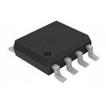
| 描述 | IC FPS PWR SWITCH VSC 8A 8-LSOP电源开关 IC - 配电 SMPS Power switch 2A, 650V |
| 产品分类 | |
| 品牌 | Fairchild Semiconductor |
| 产品手册 | |
| 产品图片 |
|
| rohs | 符合RoHS无铅 / 符合限制有害物质指令(RoHS)规范要求 |
| 产品系列 | 开关 IC,电源开关 IC - 配电,Fairchild Semiconductor FSQ0265RLXFPS™ |
| 数据手册 | |
| 产品型号 | FSQ0265RLX |
| 产品 | Power Switches |
| 产品种类 | 电源开关 IC - 配电 |
| 供应商器件封装 | 8-LSOP |
| 其它名称 | FSQ0265RLXDKR |
| 功率(W) | 20W |
| 包装 | Digi-Reel® |
| 单位重量 | 710 mg |
| 商标 | Fairchild Semiconductor |
| 安装风格 | SMD/SMT |
| 导通电阻—最大值 | 4.5 Ohmms |
| 封装 | Reel |
| 封装/外壳 | 8-SMD,鸥翼型 |
| 封装/箱体 | LSOP-8 |
| 工作温度 | -40°C ~ 85°C |
| 工作电源电压 | 26 V |
| 工厂包装数量 | 1000 |
| 开关数量 | 1 |
| 最大功率耗散 | 1.5 W |
| 最大工作温度 | + 85 C |
| 最小工作温度 | - 40 C |
| 标准包装 | 1 |
| 电压-击穿 | 650V |
| 电压-输入 | 8 V ~ 20 V |
| 电压-输出 | - |
| 电流限制 | 1.68 A |
| 电源电流—最大值 | 5 mA |
| 空闲时间—最大值 | 55 ns |
| 类型 | Power Switch |
| 系列 | FSQ0265 |
| 输出端数量 | 1 Output |
| 输出隔离 | 隔离 |
| 运行时间—最大值 | 20 ns |
| 频率范围 | 55kHz ~ 67kHz |


PDF Datasheet 数据手册内容提取
Is Now Part of To learn more about ON Semiconductor, please visit our website at www.onsemi.com Please note: As part of the Fairchild Semiconductor integration, some of the Fairchild orderable part numbers will need to change in order to meet ON Semiconductor’s system requirements. Since the ON Semiconductor product management systems do not have the ability to manage part nomenclature that utilizes an underscore (_), the underscore (_) in the Fairchild part numbers will be changed to a dash (-). This document may contain device numbers with an underscore (_). Please check the ON Semiconductor website to verify the updated device numbers. The most current and up-to-date ordering information can be found at www.onsemi.com. Please email any questions regarding the system integration to Fairchild_questions@onsemi.com. ON Semiconductor and the ON Semiconductor logo are trademarks of Semiconductor Components Industries, LLC dba ON Semiconductor or its subsidiaries in the United States and/or other countries. ON Semiconductor owns the rights to a number of patents, trademarks, copyrights, trade secrets, and other intellectual property. A listing of ON Semiconductor’s product/patent coverage may be accessed at www.onsemi.com/site/pdf/Patent-Marking.pdf. ON Semiconductor reserves the right to make changes without further notice to any products herein. ON Semiconductor makes no warranty, representation or guarantee regarding the suitability of its products for any particular purpose, nor does ON Semiconductor assume any liability arising out of the application or use of any product or circuit, and specifically disclaims any and all liability, including without limitation special, consequential or incidental damages. Buyer is responsible for its products and applications using ON Semiconductor products, including compliance with all laws, regulations and safety requirements or standards, regardless of any support or applications information provided by ON Semiconductor. “Typical” parameters which may be provided in ON Semiconductor data sheets and/or specifications can and do vary in different applications and actual performance may vary over time. All operating parameters, including “Typicals” must be validated for each customer application by customer’s technical experts. ON Semiconductor does not convey any license under its patent rights nor the rights of others. ON Semiconductor products are not designed, intended, or authorized for use as a critical component in life support systems or any FDA Class 3 medical devices or medical devices with a same or similar classification in a foreign jurisdiction or any devices intended for implantation in the human body. Should Buyer purchase or use ON Semiconductor products for any such unintended or unauthorized application, Buyer shall indemnify and hold ON Semiconductor and its officers, employees, subsidiaries, affiliates, and distributors harmless against all claims, costs, damages, and expenses, and reasonable attorney fees arising out of, directly or indirectly, any claim of personal injury or death associated with such unintended or unauthorized use, even if such claim alleges that ON Semiconductor was negligent regarding the design or manufacture of the part. ON Semiconductor is an Equal Opportunity/Affirmative Action Employer. This literature is subject to all applicable copyright laws and is not for resale in any manner.
F S Q 0 3 August 2011 6 5 / 0 2 6 5 / 0 1 FSQ0365, FSQ0265, FSQ0165, FSQ321 6 5 / 3 Green Mode Fairchild Power Switch (FPS™) 2 1 for Valley Switching Converter – Low EMI and High Efficiency — G r e e Features Description n M A Valley Switching Converter generally shows lower EMI o Optimized for Valley Switching Converter (VSC) d and higher power conversion efficiency than a e Low EMI through Variable Frequency Control and conventional hard-switched converter with a fixed F Inherent Frequency Modulation switching frequency. The FSQ-series is an integrated a i Pulse-Width Modulation (PWM) controller and r c High Efficiency through Minimum Voltage Switching SenseFET specifically designed for valley switching h operation with minimal external components. The PWM il Narrow Frequency Variation Range Over Wide Load controller includes an integrated fixed-frequency d P and Input Voltage Variation oscillator, under-voltage lockout, Leading-Edge Blanking o (LEB), optimized gate driver, internal soft-start, w Advanced Burst-Mode Operation for Low Standby temperature-compensated precise current sources for e Power Consumption loop compensation, and self-protection circuitry. r S Pulse-by-Pulse Current Limit Compared with discrete MOSFET and PWM controller w i t solutions, the FSQ-series reduces total cost, component c Protection Functions: Overload Protection (OLP), count, size and weight; while simultaneously increasing h Over-Voltage Protection (OVP), Abnormal Over- efficiency, productivity, and system reliability. This (F Current Protection (AOCP), Internal Thermal device provides a basic platform for cost-effective P Shutdown (TSD) designs of valley switching fly-back converters. S ™ Under-Voltage Lockout (UVLO) with Hysteresis ) Related Application Notes f o Internal Startup Circuit r Internal High-Voltage SenseFET: 650V AN-4137 - Design Guidelines for Offline Flyback Va Converters Using Fairchild Power Switch (FPS™) ll e Built-in Soft-Start: 15ms AN-4141 - Troubleshooting and Design Tips for y S Fairchild Power Switch (FPS™) Flyback w Applications Applications i t c Power Supplies for DVP Player, DVD Recorder, AN-4147 - Design Guidelines for RCD Snubber of hi n Set-Top Box Flyback Converters g Adapter AN-4150 - Design Guidelines for Flyback Co Converters Using FSQ-series Fairchild Power n Auxiliary Power Supply for PC, LCD TV, and PDP TV Switch (FPS™) v e r AN-4134 - Design Guidelines for Off-line Forward te Converters Using Fairchild Power Switch (FPS™) r © 2007 Fairchild Semiconductor Corporation www.fairchildsemi.com FSQ0365, FSQ0265, FSQ0165, FSQ321 • Rev. 1.0.6
F S Q Ordering Information 0 3 6 Maximum Output Table(1) 5 / Operating Current R 230V ±15%(2) 85-265V Replaces 0 Part Number Package DS(ON) AC AC 2 Temperature Limit (Max.) Open Open Devices 6 Adapter(3) Adapter(3) 5 Frame(4) Frame(4) / 0 FSQ321 8-DIP 1 6 5 FSQ321L 8-LSOP FSDL321 /3 -40 to +85°C 0.6A 19Ω 8W 12W 7W 10W 8-LSOP FSDM311 2 1 FSQ321LX (Tape & — Reel) G FSQ0165RN 8-DIP r e FSQ0165RL 8-LSOP e -40 to +85°C 0.9A 10Ω 10W 15W 9W 13W FSDL0165RN n 8-LSOP M FSQ0165RLX (Tape & o Reel) d e FSQ0265RN 8-DIP FSDM0265RN -40 to +85°C 1.2A 6Ω 14W 20W 11W 16W F FSQ0265RL 8-LSOP FSDM0265RNB a i r FSQ0365RN 8-DIP FSDM0365RN c -40 to +85°C 1.5A 4.5Ω 17.5W 25W 13W 19W h FSQ0365RL 8-LSOP FSDM0365RNB il d Notes: P 1. The junction temperature can limit the maximum output power. o 2. 230V or 100/115V with voltage doubler. The maximum power with CCM operation w AC AC e 3. Typical continuous power in a non-ventilated, enclosed adapter measured at 50C ambient temperature. r 4. Maximum practical continuous power in an open-frame design at 50C ambient temperature. S w i t c h ( F P S ™ ) f o r V a l l e y S w i t c h i n g C o n v e r t e r © 2007 Fairchild Semiconductor Corporation www.fairchildsemi.com FSQ0365, FSQ0265, FSQ0165, FSQ321 • Rev. 1.0.6 2
F Application Circuit S Q 0 Vo 3 6 5 / 0 2 6 AC 5 IN / 0 1 Vstr 6 Drain 5 / 3 PWM 2 Sync GND 1 — Vfb Vcc G r e e n M o d e F a i r Figure 1. Typical Flyback Application c h i ld P o w Internal Block Diagram e r S Sync Vstr Vcc Drain w 4 5 2 6 7 8 it c h + 0.7V/0.2V OSC (F - P + S + 0.35/0.55 Vref ™ VCC Vref VBurst - VCCGood - 8V/12V ) f o Vfb Idelay IFB 3R PWM r V 3 S Q a R SStoafrt-t 2L0E0nBs R Q DGriavteer lley S w i t c h i n AOCP g 1 C 6V TSD S Q VOCP GND o VSD (1.1V) n 2.5 s Time R Q v Sync Delay e Vovp6V VCCGood rter FSQ0365RN Rev.00 Figure 2. Internal Block Diagram © 2007 Fairchild Semiconductor Corporation www.fairchildsemi.com FSQ0365, FSQ0265, FSQ0165, FSQ321 • Rev. 1.0.6 3
F Pin Assignments S Q 0 3 6 5 / 0 2 6 5 / 0 1 6 5 / 3 2 1 — G r Figure 3. Pin Configuration (Top View) e e n M o Pin Definitions d e Pin# Name Description F a i 1 GND SenseFET source terminal on primary side and internal control ground. rc h Positive supply voltage input. Although connected to an auxiliary transformer winding, i l current is supplied from pin 5 (Vstr) via an internal switch during startup (see Figure 2). d 2 V CC It is not until V reaches the UVLO upper threshold (12V) that the internal startup switch P CC o opens and device power is supplied via the auxiliary transformer winding. w The feedback voltage pin is the non-inverting input to the PWM comparator. It has a e r 0.9mA current source connected internally while a capacitor and opto-coupler are typically S connected externally. There is a time delay while charging external capacitor C from 3V w 3 Vfb fb to 6V using an internal 5A current source. This delay prevents false triggering under it c transient conditions, but still allows the protection mechanism to operate under true h overload conditions. ( F This pin is internally connected to the sync-detect comparator for valley switching. P S Typically the voltage of the auxiliary winding is used as Sync input voltage and external 4 Sync ™ resistors and capacitor are needed to make delay to match valley point. The threshold of ) the internal sync comparator is 0.7V/0.2V. f o This pin is connected to the rectified AC line voltage source. At startup, the internal switch r 5 Vstr supplies internal bias and charges an external storage capacitor placed between the Vcc V a pin and ground. Once the VCC reaches 12V, the internal switch is opened. ll e The drain pins are designed to connect directly to the primary lead of the transformer and y 6, 7, 8 Drain are capable of switching a maximum of 650V. Minimizing the length of the trace S connecting these pins to the transformer decreases leakage inductance. w i t c h i n g C o n v e r t e r © 2007 Fairchild Semiconductor Corporation www.fairchildsemi.com FSQ0365, FSQ0265, FSQ0165, FSQ321 • Rev. 1.0.6 4
F Absolute Maximum Ratings S Q Stresses exceeding the absolute maximum ratings may damage the device. The device may not function or be 0 3 operable above the recommended operating conditions and stressing the parts to these levels is not recommended. 6 In addition, extended exposure to stresses above the recommended operating conditions may affect device reliability. 5 / 0 The absolute maximum ratings are stress ratings only. T =25°C, unless otherwise specified. A 2 6 5 Symbol Parameter Min. Max. Unit / 0 1 V Vstr Pin Voltage 500 V STR 6 5 VDS Drain Pin Voltage 650 V /3 2 V Supply Voltage 20 V CC 1 V Feedback Voltage Range -0.3 9.0 V — FB V Sync Pin Voltage -0.3 9.0 V G Sync r FSQ0365 12.0 e e FSQ0265 8.0 n I Drain Current Pulsed(6) A M DM FSQ0165 4.0 o d FSQ321 1.5 e FSQ0365 230 F a FSQ0265 140 ir E Single Pulsed Avalanche Energy(7) mJ c AS FSQ0165 50 h i l d FSQ321 10 P P Total Power Dissipation 1.5 W o D w TJ Recommended Operating Junction Temperature -40 Internally Limited C er TA Operating Ambient Temperature -40 +85 C S w T Storage Temperature -55 +150 C STG i t Human Body Model; JESD22-A114 CLASS 1C c h ESD Machine Model; JESD22-A115 CLASS B ( F Notes: P S 5. Repetitive rating: Pulse width limited by maximum junction temperature. ™ 6. L=51mH, starting TJ=25°C. ) f o r V a Thermal Impedance l l e y Symbol Parameter Value Unit S w 8-DIP(7) i t c θ Junction-to-Ambient Thermal Resistance(8) 80 h JA i θ Junction-to-Case Thermal Resistance(9) 20 °C/W n JC g θ Junction-to-Top Thermal Resistance(10) 35 C JT o Notes: n 7. All items are tested with the standards JESD 51-2 and 51-10 (DIP). v e 8. Free-standing with no heat-sink, under natural convection. r t 9. Infinite cooling condition - refer to the SEMI G30-88. e r 10. Measured on the package top surface. © 2007 Fairchild Semiconductor Corporation www.fairchildsemi.com FSQ0365, FSQ0265, FSQ0165, FSQ321 • Rev. 1.0.6 5
F S Electrical Characteristics Q 0 3 T A=25C unless otherwise specified. 65 / Symbol Parameter Condition Min. Typ. Max. Unit 0 2 6 SenseFET Section 5 / BV Drain-Source Breakdown Voltage V =0V, I =100µA 650 V 0 DSS CC D 1 6 IDSS Zero-Gate-Voltage Drain Current VDS=650V 100 µA 5 / FSQ0365 3.5 4.5 3 2 1 Drain-Source On- FSQ0265 5.0 6.0 RDS(ON) State Resistance(11) FSQ0165 TJ=25C, ID=0.5A 8.0 10.0 — G FSQ321 14.0 19.0 r e FSQ0365 315 e n FSQ0265 550 M CISS Input Capacitance VGS=0V, VDS=25V, f=1MHz pF o FSQ0165 250 d e FSQ321 162 F FSQ0365 47 a i r FSQ0265 38 c h C Output Capacitance V =0V, V =25V, f=1MHz pF OSS GS DS i FSQ0165 25 l d FSQ321 18 P o FSQ0365 9.0 w e Reverse Transfer FSQ0265 17.0 r CRSS Capacitance FSQ0165 VGS=0V, VDS=25V, f=1MHz 10.0 pF Sw i FSQ321 3.8 t c h FSQ0365 11.2 ( F FSQ0265 20.0 P t Turn-On Delay V =350V, I =25mA ns d(on) DD D S FSQ0165 12.0 ™ FSQ321 9.5 ) f FSQ0365 34 o r FSQ0265 15 V t Rise Time V =350V, I =25mA ns a r FSQ0165 DD D 4 ll e y FSQ321 19 S FSQ0365 28.2 w i FSQ0265 55.0 tc td(off) Turn-Off Delay VDD=350V, ID=25mA ns h FSQ0165 30.0 i n g FSQ321 33.0 C FSQ0365 32 o n FSQ0265 25 v t Fall Time V =350V, I =25mA ns e f DD D FSQ0165 10 r t e FSQ321 42 r Burst-Mode Section V 0.45 0.55 0.65 V BURH V Burst-Mode Voltage T =25°C, t =200ns(12) 0.25 0.35 0.45 V BURL J PD V 200 mV BUR(HYS) Continued on the following page… © 2007 Fairchild Semiconductor Corporation www.fairchildsemi.com FSQ0365, FSQ0265, FSQ0165, FSQ321 • Rev. 1.0.6 6
F Electrical Characteristics (Continued) S Q T =25C unless otherwise specified. 0 A 3 6 Symbol Parameter Conditions Min. Typ. Max. Unit 5 / 0 Control Section 2 6 All but 5 tON.MAX1 Maximum On Time1 FSQ321 TJ=25°C 10.5 12.0 13.5 µs /0 1 t Maximum On Time2 FSQ321 T =25°C 6.35 7.06 7.77 µs 6 ON.MAX2 J 5 All but /3 tB1 Blanking Time1 FSQ321 13.2 15.0 16.8 µs 2 1 t Blanking Time2 FSQ321 7.5 8.2 µs — B2 t Detection Time Window T =25°C, V =0V 3.0 µs G W J sync r f Switching Frequency Variation(14) -25C < T < 85C ±5 ±10 % e S J e I Feedback Source Current V =0V 700 900 1100 µA n FB FB M DMIN Minimum Duty Cycle VFB=0V 0 % o d V 11 12 13 V START e UVLO Threshold Voltage After Turn-on V 7 8 9 V F STOP a All but With Free-Running ir tS/S1 Internal Soft-Start Time 1 FSQ321 Frequency 15 ms ch i With Free-Running ld tS/S2 Internal Soft-Start Time 2 FSQ321 Frequency 10 ms P o Protection Section w e FSQ0365 TJ=25°C, di/dt=240mA/µs 1.32 1.50 1.68 r S FSQ0265 T =25°C, di/dt=200mA/µs 1.06 1.20 1.34 J w I Peak Current Limit A LIM FSQ0165 TJ=25°C, di/dt=175mA/µs 0.8 0.9 1.0 itc h FSQ321 T =25°C, di/dt=125mA/µs 0.53 0.60 0.67 J ( F V Shutdown Feedback Voltage V =15V 5.5 6.0 6.5 V SD CC P I Shutdown Delay Current V =5V 4.0 5.0 6.0 µA S DELAY FB ™ tLEB Leading-Edge Blanking Time(13) 200 ns ) f V Over-Voltage Protection V =15V, V =2V 5.5 6.0 6.5 V o OVP CC FB r Over-Voltage Protection Blanking V tOVP Time 2 3 4 µs a l l TSD Thermal Shutdown Temperature(13) 125 140 155 °C ey Sync Section S w V 0.55 0.70 0.85 V i SH t Sync Threshold Voltage c V 0.14 0.20 0.26 V h SL i n tSync Sync Delay Time(13,14) 300 ns g Total Device Section C o Operating Supply Current n IOP (Control Part Only) VCC=15V 1 3 5 mA ve r I Start Current VCC=VSTART - 0.1V 270 360 450 µA te START (Before V Reaches V ) r CC START I Startup Charging Current V =0V, V =Minimum 40V 0.65 0.85 1.00 mA CH CC STR V Minimum V Supply Voltage 26 V STR STR Notes: 11. Pulse test: Pulse-Width=300s, duty=2%. 12. Propagation delay in the control IC. 13. Though guaranteed, it is not 100% tested in production. 14. Includes gate turn-on time. © 2007 Fairchild Semiconductor Corporation www.fairchildsemi.com FSQ0365, FSQ0265, FSQ0165, FSQ321 • Rev. 1.0.6 7
F S Q Comparison Between FSDM0x65RNB and FSQ-Series 0 3 6 Function FSDM0x65RNB FSQ-Series Advantages of FSQ-Series 5 / 0 Operation Method Constant Valley Switching Improved efficiency by valley switching 26 Frequency PWM Operation Reduced EMI noise 5/ 0 1 Valley Switching & Frequency 6 EMI Reduction Inherent Frequency Reduce EMI noise in two ways 5 Modulation / Modulation 3 2 Improved standby power by valley switching also in 1 — burst-mode Burst-Mode Advanced Burst- Operation Fixed Burst Peak Mode Because the current peak during burst operation is Gr dependent on V , it is easier to solve audible e FB e noise n M Improved reliability through precise abnormal over- Protection AOCP o current protection d e F a i r c h i l d P o w e r S w i t c h ( F P S ™ ) f o r V a l l e y S w i t c h i n g C o n v e r t e r © 2007 Fairchild Semiconductor Corporation www.fairchildsemi.com FSQ0365, FSQ0265, FSQ0165, FSQ321 • Rev. 1.0.6 8
F Typical Performance Characteristics S Q Characteristic graphs are normalized at T =25°C. 0 A 3 6 5 / 0 2 1.2 1.2 6 5 1.0 1.0 /0 1 ed 0.8 ed 0.8 6 z z 5 mali 0.6 mali 0.6 /3 Nor 0.4 Nor 0.4 21 — 0.2 0.2 G r 0.0 0.0 e -25 0 25 50 75 100 125 -25 0 25 50 75 100 125 e n Temperature [°C] Temperature [°C] M o Figure 4. Operating Supply Current (IOP) vs. TA Figure 5. UVLO Start Threshold Voltage (VSTART) d vs. T e A F a i rc 1.2 1.2 h i l d 1.0 1.0 P zed 0.8 zed 0.8 ow mali 0.6 mali 0.6 er or or S N 0.4 N 0.4 w i 0.2 0.2 tc h 0.0 0.0 ( -25 0 25 50 75 100 125 -25 0 25 50 75 100 125 F P Temperature [°C] Temperature [°C] S ™ Figure 6. UVLO Stop Threshold Voltage (VSTOP) Figure 7. Startup Charging Current (ICH) vs. TA ) vs. TA fo r V a l l 1.2 1.2 e y 1.0 1.0 S w malized 00..68 malized 00..68 itchi or or n N 0.4 N 0.4 g C 0.2 0.2 o n 0.0 0.0 v -25 0 25 50 75 100 125 -25 0 25 50 75 100 125 e r Temperature [°C] Temperature [°C] te r Figure 8. Initial Switching Frequency (f ) vs. T Figure 9. Maximum On Time (t ) vs. T S A ON.MAX A © 2007 Fairchild Semiconductor Corporation www.fairchildsemi.com FSQ0365, FSQ0265, FSQ0165, FSQ321 • Rev. 1.0.6 9
F Typical Performance Characteristics (Continued) S Q Characteristic graphs are normalized at T =25°C. 0 A 3 6 5 / 0 2 1.2 1.2 6 5 1.0 1.0 /0 1 ed 0.8 ed 0.8 6 z z 5 mali 0.6 mali 0.6 /3 Nor 0.4 Nor 0.4 21 — 0.2 0.2 G r 0.0 0.0 e -25 0 25 50 75 100 125 -25 0 25 50 75 100 125 e n Temperature [°C] Temperature [°C] M o Figure 10. Blanking Time (tB) vs. TA Figure 11. Feedback Source Current (IFB) vs. TA d e F a i 1.2 1.2 rc h 1.0 1.0 il d ed 0.8 ed 0.8 P maliz 0.6 maliz 0.6 ow or or e N 0.4 N 0.4 r S w 0.2 0.2 i t c 0.0 0.0 h -25 0 25 50 75 100 125 -25 0 25 50 75 100 125 ( Temperature [°C] Temperature [°C] F P S Figure 13. Burst Mode High Threshold Voltage (V ) ™ Figure 12. Shutdown Delay Current (I ) vs. T burh DELAY A vs. TA ) f o r V 1.2 1.2 a l l e 1.0 1.0 y malized 00..68 malized 00..68 Switc or or h N 0.4 N 0.4 in g 0.2 0.2 C o 0.0 0.0 n -25 0 25 50 75 100 125 -25 0 25 50 75 100 125 v Temperature [°C] Temperature [°C] e r t e Figure 14. Burst Mode Low Threshold Voltage (Vburl) Figure 15. Peak Current Limit (ILIM) vs. TA r vs. T A © 2007 Fairchild Semiconductor Corporation www.fairchildsemi.com FSQ0365, FSQ0265, FSQ0165, FSQ321 • Rev. 1.0.6 10
F Typical Performance Characteristics (Continued) S Q Characteristic graphs are normalized at T =25°C. 0 A 3 6 5 / 0 2 1.2 1.2 6 5 1.0 1.0 /0 1 ed 0.8 ed 0.8 6 z z 5 mali 0.6 mali 0.6 /3 Nor 0.4 Nor 0.4 21 — 0.2 0.2 G r 0.0 0.0 e -25 0 25 50 75 100 125 -25 0 25 50 75 100 125 e n Temperature [°C] Temperature [°C] M o Figure 16. Sync High Threshold (VSH) vs. TA Figure 17. Sync Low Threshold Voltage (VSL) vs. TA d e F a i 1.2 1.2 rc h 1.0 1.0 il d d d e 0.8 e 0.8 P maliz 0.6 maliz 0.6 ow or or e N 0.4 N 0.4 r S w 0.2 0.2 i t c 0.0 0.0 h -25 0 25 50 75 100 125 -25 0 25 50 75 100 125 ( Temperature [°C] Temperature [°C] F P S Figure 18. Shutdown Feedback Voltage (V ) vs. T Figure 19. Over-Voltage Protection (V ) vs. T ™ SD A OP A ) f o r V a l l e y S w i t c h i n g C o n v e r t e r © 2007 Fairchild Semiconductor Corporation www.fairchildsemi.com FSQ0365, FSQ0265, FSQ0165, FSQ321 • Rev. 1.0.6 11
F Functional Description S Q 1. Startup: At startup, an internal high-voltage current 0 3 source supplies the internal bias and charges the VCC Vref 6 external capacitor (Ca) connected to the VCC pin, as Idelay IFB 5/ 0 iFllPusSt™rat ebde ginin sF isgwuritec h2in0g. Wanhde nth eV CiCn terernaaclh ehsig h1-2vVo,l tatghee VO FOD817A VFB 3 D1 D2 OSC SenseFET 26 current source is disabled. The FPS continues its CB 3R 5/ 0 normal switching operation and the power is supplied + Gate 1 from the auxiliary transformer winding unless V goes VFB* R driver 6 below the stop voltage of 8V. CC KA431 - 5/ 3 2 VDC VSD OLP Rsense 1 — FSQ0365RNRev. 00 G C a Figure 21. Pulse-Width-Modulation (PWM) Circuit re e 3. Synchronization: The FSQ-series employs a valley n 2 VCC 5 Vstr slowsistc. hiTnhge t ecbhansiiqc uew taov emfoinrimmsiz eo ft heth sew itvcahllienyg nsowisitec hainngd Mo d converter are shown in Figure 22. To minimize the e ICH MOSFET's switching loss, the MOSFET should be F turned on when the drain voltage reaches its minimum a 8V/12V V good Vref value, as shown in Figure 22. The minimum drain irc CC voltage is indirectly detected by monitoring the V h CC i winding voltage, as shown in Figure 22. l Internal d Bias P V FSQ0365RN Rev.00 ds o w Figure 20. Startup Circuit e VRO r 2. Feedback Control: FPS employs Current Mode S cFoOnDtr8o1l,7 aAs) sahnodw ns ihnu Fnitg urereg u2l1a.t oAr n( soupctoh- caosu pKleAr 4(s3u1c) ha ares VDC VRO wit c often used to implement the feedback network. h Cthoem RpaSEriNnSgE threes fiesetodrb amcak kveosl taitg ep wositshi bthlee tvoo ltcaognet raocl rothses Vsync tF V (6V) (FP switching duty cycle. When the reference pin voltage of ovp S ™ the shunt regulator exceeds the internal reference voltage of 2.5V, the opto-coupler LED current increases, ) f pulling down the feedback voltage and reducing the duty 0.7V o r cycle. This event typically occurs when input voltage is 0.2V V increased or output load is decreased. 300ns Delay a l l 2.1 Pulse-by-Pulse Current Limit: Because Current MOSFET Gate e y Mode control is employed, the peak current through the S SenseFET is limited by the inverting input of PWM w comparator (VFB*), as shown in Figure 21. Assuming ON ON it that the 0.9mA current source flows only through the c h internal resistor (3R + R = 2.8kΩ), the cathode voltage FSQ0365RN Rev.00 in of diode D2 is about 2.5V. Since D1 is blocked when the g feedback voltage (VFB) exceeds 2.5V, the maximum Figure 22. Valley Resonant Switching Waveforms C voltage of the cathode of D2 is clamped at this voltage, 4. Protection Circuits: The FSQ-series has several o clamping V *. Therefore, the peak value of the current n FB self-protective functions, such as Overload Protection v through the SenseFET is limited. (OLP), Abnormal Over-Current protection (AOCP), e r 2.2 Leading-Edge Blanking (LEB): At the instant the Over-Voltage Protection (OVP), and Thermal Shutdown te internal SenseFET is turned on, a high-current spike (TSD). All the protections are implemented as Auto- r usually occurs through the SenseFET, caused by Restart Mode. Once the fault condition is detected, primary-side capacitance and secondary-side rectifier switching is terminated and the SenseFET remains off. reverse recovery. Excessive voltage across the Rsense This causes VCC to fall. When VCC falls down to the resistor would lead to incorrect feedback operation in the Under-Voltage Lockout (UVLO) stop voltage of 8V, the Current Mode PWM control. To counter this effect, the protection is reset and the startup circuit charges the FPS employs a leading-edge blanking (LEB) circuit. This VCC capacitor. When the VCC reaches the start voltage circuit inhibits the PWM comparator for a short time of 12V, the FSQ-series resumes normal operation. If the (t ) after the SenseFET is turned on. fault condition is not removed, the SenseFET remains LEB off and V drops to stop voltage again. In this manner, CC © 2007 Fairchild Semiconductor Corporation www.fairchildsemi.com FSQ0365, FSQ0265, FSQ0165, FSQ321 • Rev. 1.0.6 12
tshwei tcahuitnog- reostfa rtt hcea np aolwteerrn atSeelyn seenFaEbTle aunndti l disthaeb lef athuelt VFB FSQ0365RN Rev.00 FS Overload protection Q condition is eliminated. Because these protection 0 circuits are fully integrated into the IC without external 3 6.0V 6 components, the reliability is improved without 5 increasing cost. /0 2 6 Fault 2.8V 5 occurs Fault / VDS Poowner removed 01 6 t12= CFB*(6.0-2.8)/Idelay 5 / 3 t t t 2 1 2 1 — Figure 24. Overload Protection G 4.2 Abnormal Over-Current Protection (AOCP): When r VCC the secondary rectifier diodes or the transformer pins ee are shorted, a steep current with extremely high-di/dt n can flow through the SenseFET during the LEB time. M 12V Even though the FSQ-series has Overload Protection o d (OLP), it is not enough to protect the FSQ-series in that 8V e abnormal case, since severe current stress is imposed F on the SenseFET until OLP triggers. The FSQ-series a t has an internal Abnormal Over-Current Protection ir c (AOCP) circuit as shown in Figure 25. When the gate h Normal Fault Normal turn-on signal is applied to the power SenseFET, the il FSQ0365RN Rev. 00 operation situation operation AOCP block is enabled and monitors the current d P Figure 23. Auto-Restart Protection Waveforms through the sensing resistor. The voltage across the o resistor is compared with a preset AOCP level. If the w 4.1 Overload Protection (OLP): Overload is defined as sensing resistor voltage is greater than the AOCP level, e r the load current exceeding its normal level due to an the set signal is applied to the latch, resulting in the S unexpected abnormal event. In this situation, the shutdown of the SMPS. w protection circuit should trigger to protect the SMPS. i t However, even when the SMPS is in the normal c h operation, the overload protection circuit can be 3R ( triggered during load transition. To avoid this undesired OSC F P operation, the overload protection circuit is designed to PWM S Q S trigger only after a specified time to determine whether it LEB Gate ™ is a transient situation or a true overload situation. 200ns R Q driver ) Because of the pulse-by-pulse current limit capability, R f o the maximum peak current through the SenseFET is r limited, and therefore the maximum input power is V restricted with a given input voltage. If the output + Rsense 1 al l consumes more than this maximum power, the output AOCP GND e voltage (VO) decreases below the set voltage. This FSQ0365RN Rev.00 - VOCP y S reduces the current through the opto-coupler LED, w which also reduces the opto-coupler transistor current, Figure 25. Abnormal Over-Current Protection i t thus increasing the feedback voltage (V ). If V c FB FB h exceeds 2.8V, D1 is blocked and the 5µA current source i n starts to charge CB slowly up to V . In this condition, CC g V continues increasing until it reaches 6V, when the FB C switching operation is terminated, as shown in Figure o 24. The delay for shutdown is the time required to n v charge CB from 2.8V to 6V with 5µA. A 20 ~ 50ms delay e is typical for most applications. r t e r © 2007 Fairchild Semiconductor Corporation www.fairchildsemi.com FSQ0365, FSQ0265, FSQ0165, FSQ321 • Rev. 1.0.6 13
F S 4.3 Over-Voltage Protection (OVP): If the secondary- V Q side feedback circuit malfunctions or a solder defect O 0 causes an opening in the feedback path, the current VOset 3 6 through the opto-coupler transistor becomes almost 5 zero. Then V climbs up in a similar manner to the /0 FB 2 overload situation, forcing the preset maximum current V FB 6 to be supplied to the SMPS until the overload protection 5 / triggers. Because more energy than required is provided 0.55V 0 1 to the output, the output voltage may exceed the rated 0.35V 6 voltage before the overload protection triggers, resulting 5 / in the breakdown of the devices in the secondary side. 3 I 2 To prevent this situation, an OVP circuit is employed. In DS 1 general, the peak voltage of the sync signal is — proportional to the output voltage and the FSQ-series G uses a sync signal instead of directly monitoring the r output voltage. If the sync signal exceeds 6V, an OVP is e e triggered, shutting down the SMPS. To avoid undesired n triggering of OVP during normal operation, the peak VDS M voltage of the sync signal should be designed below 6V. o d 4.4 Thermal Shutdown (TSD): The SenseFET and the e control IC are built in one package. This makes it easy F for the control IC to detect the abnormal over time a i r temperature of the SenseFET. If the temperature Switching Switching c exceeds ~150°C, the thermal shutdown triggers. FSQ0365RN Rev.00 t1 disabled t2 t3 disabled t4 hi l d 5. Soft-Start: An internal soft-start circuit increases Figure 26. Waveforms of Burst Operation P PWM comparator inverting input voltage with the o 7. Switching Frequency Limit: To minimize switching SenseFET current slowly after it starts up. The typical w soft-start time is 15ms. The pulsewidth to the power loss and Electromagnetic Interference (EMI), the e MOSFET turns on when the drain voltage reaches its r switching device is progressively increased to establish S minimum value in valley switching operation. However, the correct working conditions for transformers, w this causes switching frequency to increases at light inductors, and capacitors. The voltage on the output it load conditions. As the load decreases, the peak drain c capacitors is progressively increased with the intention h current diminishes and the switching frequency of smoothly establishing the required output voltage. ( increases. This results in severe switching losses at F This helps prevent transformer saturation and reduces light-load condition, as well as intermittent switching and P stress on the secondary diode during startup. S audible noise. Because of these problems, the valley ™ 6. Burst Operation: To minimize power dissipation in switching converter topology has limitations in a wide ) Standby Mode, the FPS enters Burst-Mode operation. range of applications. f o As the load decreases, the feedback voltage decreases. r As shown in Figure 26, the device automatically enters To overcome this problem, FSQ-series employs a V Burst Mode when the feedback voltage drops below frequency-limit function, as shown in Figure 27 and a VouBtUpRuL t (3vo5l0tamgVe)s. Astta rtth isto pdorionpt, aswt iatc hraintge sdteoppesn daenndt tohne Ftuigrnu-roen 2is8 . pOronhcibei tethde dSuerinnsge tFhEeT b lias ntkuirnnge dti moen ,( ttBh)e. Anfetexrt lley standby current load. This causes the feedback voltage the blanking time, the controller finds the valley within S the detection time window (t ) and turns on the w to rise. Once it passes V (550mV), switching W resumes. The feedback voltBaUgReH then falls and the MOSFET, as shown in Figure 27 and Figure 28 (cases itc process repeats. Burst Mode alternately enables and A, B, and C). If no valley is found during tW, the internal h disables switching of the power SenseFET, reducing SenseFET is forced to turn on at the end of tW (case D). in Therefore, FSQ devices have a minimum switching g switching loss in Standby Mode. frequency of 55kHz and a maximum switching frequency C of 67kHz, as shown in Figure 28. o n v e r t e r © 2007 Fairchild Semiconductor Corporation www.fairchildsemi.com FSQ0365, FSQ0265, FSQ0165, FSQ321 • Rev. 1.0.6 14
F S Q tmax=18s When the resonant period is 2s 0 s 67kHz 3 IDS IDS A B C Constant 65 59kHz frequency /0 55kHz 2 A D 6 5 t =15s /0 B 1 Burst 6 mode 5 ts /3 2 1 I I — DS DS G B PO re FSQ0365RN Rev. 00 e n tB=15s Figure 28. Switching Frequency Range M o d t s e F a i r c h IDS IDS ild P C o w e t =15s r B S w t i s t c h ( F P I I S DS DS ™ ) f o r D V t =15s B t =3s a W ll e y S tmax=18s w s FSQ0365RN Rev. 00 i t c Figure 27. Valley Switching with Limited Frequency h i n g C o n v e r t e r © 2007 Fairchild Semiconductor Corporation www.fairchildsemi.com FSQ0365, FSQ0265, FSQ0165, FSQ321 • Rev. 1.0.6 15
F S Q Typical Application Circuit of FSQ0365RN 0 3 6 5 / 0 Input Voltage Output Voltage 2 Application FPS Device Rated Output Power Range (Maximum Current) 6 5 / 5.1V (1.0A) 0 1 DVD Player FSQ0365RN 85-265V 19W 3.4V (1.0A) 65 Power Supply AC 12V (0.4A) /3 2 16V (0.3A) 1 — Features G High efficiency ( >77% at universal input) r e Low standby mode power consumption (<1W at 230VAC input and 0.5W load) en Reduce EMI noise through Valley Switching operation M o Enhanced system reliability through various protection functions d e Internal soft-start: 15ms F a i r Key Design Notes c h The delay time for overload protection is designed to be about 30ms with C107 of 47nF. If faster/slower triggering il d of OLP is required, C107 can be changed to a smaller/larger value (eg. 100nF for 60ms). P The input voltage of V must be higher than -0.3V. By proper voltage sharing by R106 & R107 resistors, the input o sync w voltage can be adjusted. e r The SMD-type 100nF capacitor must be placed as close as possible to VCC pin to avoid malfunction by abrupt S pulsating noises and to improved surge immunity. w i t c Schematic h C209 (F EETR1208128 47pF L201 PS 16V, 0.3A RT101 1 11 D201 C201 C202 ™ 5D-9 UF4003 470F 470F ) 1R0100k5Ω 5R61k0Ω2 C101n0F4 2 C472p1F0 35V 35V fo C4303100VF3 6R361020VΩ8 1ND 1400107 3 10 D202 C2L02302 C204 12V, 0.4A r Va 2 FSQIC0130615RN 12UF4003 43750VF 43750VF lle 1 BBDrDiiod1dg0e1e 3 45SVysntrc DDDrrraaaiiinnn678 1C0100n6FC2210F7 R103 6 L203 5.1V, 1A y Sw 100nCF41,20725VAC C471n0F5 3FBGND1Vcc 2 SMD 501VND 1400204 R51Ω04 4 SDB230630 1C0102000V5F 1C0102000V6F itchi 50V 12kΩ 5 L204 n 9 g ZD101 3.4V, 1A 1N4746A C110 D204 C207 C208 C L4F0m10H1 3530pVF 6.2kΩ6.2kΩR106R107 1N4148D103 8 SB360 10 1000VF 101000VF onver C302 t 3.3nF R201 e C101 510Ω r 100nF R203 275VAC 6.2kΩ R202 1kΩ R204 C209 20kΩ 100nF IC202 TNR FOD817A 10D471K F101 FUSE IC201 R205 KA431 6kΩ AC IN FSQ0365RN Rev:00 Figure 29. Demo Circuit of FSQ0365RN © 2007 Fairchild Semiconductor Corporation www.fairchildsemi.com FSQ0365, FSQ0265, FSQ0165, FSQ321 • Rev. 1.0.6 16
F S Q Transformer 0 3 6 5 / EER2828 0 12 2 6 N /2 1 p 5 Np/2 11N16V N16V /01 Np/2 2 10N N 65 12V 12V /3 3 9 N3.4V Na 21 Na 4 8 N5.1V — 6mm 3mm G 5 7 N3.4V re N /2 e p n 6 N 5.1V M FSQ0365RN Rev: 00 o d Figure 30. Transformer Schematic Diagram of FSQ0365RN e F a Table 1. Winding Specification i r c No. Pin (sf) Wire Turns Winding Method h i l d Np/2 32 0.25 x 1 50 Center Solenoid Winding P Insulation: Polyester Tape t = 0.050mm, 2-Layer o w N 98 0.33 x 2 4 Center Solenoid Winding e 3.4V r Insulation: Polyester Tape t = 0.050mm, 2-Layer S w N5V 69 0.33 x 1 2 Center Solenoid Winding it c Insulation: Polyester Tape t = 0.050mm, 2-Layer h ( N 45 0.25 x 1 16 Center Solenoid Winding F a P Insulation: Polyester Tape t = 0.050mm, 2-Layer S ™ N12V 1012 0.33 x 3 14 Center Solenoid Winding ) f Insulation: Polyester Tape t = 0.050mm, 3-Layer o r N 1112 0.33 x 3 18 Center Solenoid Winding V 16V a l Insulation: Polyester Tape t = 0.050mm, 2-Layer l e y Np/2 21 0.25 x 1 50 Center Solenoid Winding S Insulation: Polyester Tape t = 0.050mm, 2-Layer w i t c h i Table 2. Electrical Characteristics n g Pin Specification Remarks C o n Inductance 1 - 3 1.4mH ± 10% 100kHz, 1V v e Leakage 1 - 3 25µH Maximum Short All Other Pins r t e Core & Bobbin r Core: EER2828 (Ae=86.66mm2) Bobbin: EER2828 © 2007 Fairchild Semiconductor Corporation www.fairchildsemi.com FSQ0365, FSQ0265, FSQ0165, FSQ321 • Rev. 1.0.6 17
F S Q Table 3. Demo Board Part List 0 3 Part Value Note Part Value Note 6 5 / Resistor Inductor 0 2 6 R102 56k(cid:31) 1W L201 10µH 5 / 0 R103 5(cid:31) 1/2W L202 10µH 1 6 R104 12k(cid:31) 1/4W L203 4.9µH 5 / 3 R105 100k(cid:31) 1/4W L204 4.9µH 2 1 R106 6.2k(cid:31) 1/4W Diode — R107 6.2k(cid:31) 1/4W D101 IN4007 G R108 62(cid:31) 1W D102 IN4004 re e R201 510(cid:31) 1/4W ZD101 1N4746A n M R202 1k(cid:31) 1/4W D103 1N4148 o d R203 6.2k(cid:31) 1/4W D201 UF4003 e R204 20k(cid:31) 1/4W D202 UF4003 F a R205 6k(cid:31) 1/4W D203 SB360 ir c Capacitor D204 SB360 h i l d C101 100nF/275VAC Box Capacitor P C102 100nF/275V Box Capacitor IC o AC w C103 33µF/400V Electrolytic Capacitor IC101 FSQ0365RN FPS™ e r C104 10nF/630V Film Capacitor IC201 KA431 (TL431) Voltage reference S w C105 47nF/50V Mono Capacitor IC202 FOD817A Opto-coupler i t c C106 100nF/50V SMD (1206) Fuse h ( C107 22µF/50V Electrolytic Capacitor Fuse 2A/250V F P C110 33pF/50V Ceramic Capacitor NTC S ™ C201 470µF/35V Electrolytic Capacitor RT101 5D-9 ) f C202 470µF/35V Electrolytic Capacitor Bridge Diode o r C203 470µF/35V Electrolytic Capacitor BD101 2KBP06M2N257 Bridge Diode V a C204 470µF/35V Electrolytic Capacitor Line Filter ll e y C205 1000µF/10V Electrolytic Capacitor LF101 40mH S C206 1000µF/10V Electrolytic Capacitor Transformer w i t C207 1000µF/10V Electrolytic Capacitor T101 c h C208 1000µF/10V Electrolytic Capacitor Varistor in g C209 100nF /50V Ceramic Capacitor TNR 10D471K C o n v e r t e r © 2007 Fairchild Semiconductor Corporation www.fairchildsemi.com FSQ0365, FSQ0265, FSQ0165, FSQ321 • Rev. 1.0.6 18
10.00 A 9.10 7.62 0.56 2.54 2.00 0.36 B 8 5 6.60 9.90 6.70 10.70 6.20 9.30 1 4 1.09 0.56 0.94 1.252 1.62 0.10 M C B A 1.784 1.47 0.56 0.10 M C B A LAND PATTERN RECOMMENDATION 0.36 TOP VIEW 7.62 A 3.60 3.20 3.70 MAX 0.10 C 2.54 0.35 0.10 MIN C 0.20 7.62 SIDE VIEW FRONT VIEW NOTES: UNLESS OTHERWISE SPECIFIED 9° A. NO INDUSTRY STANDARD APPLIES TO THIS PACKAGE R0.20 B. ALL DIMENSIONS ARE IN MILLIMETERS R0.20 C. DIMENSIONS ARE EXCLUSIVE OF BURRS, MOLD FLASH, AND TIE BAR EXTRUSIONS GAGE PLANE D. DIMENSIONS AND TOLERANCES PER 0.25 8° ASME Y14.5M-2009 0° E. DRAWING FILENAME: MKT-MLSOP08Arev2 1.12 0.72 SEATING 3° PLANE 1.60 REF DETAIL A SCALE 2:1
0.400 10.16 A 0.373 9.47 C 0.036 0.9 TYP 8 5 8 R0.032 0.813 0.092 2.337 0.255 6.48 PIN #1 PIN #1 0.245 6.22 C 1 4 1 B TOP VIEW, OPTION 1 TOP VIEW, OPTION 2 D 0.320 8.13 7° TYP 0.070 1.78 0.300 7.62 0.045 1.14 7° TYP 0.135 3.43 0.210 5.33 MAX 0.125 3.18 0.015 0.381 0.010 0.254 C 0.060 1.52 0.015 0.38 MIN MAX 0.140 3.56 0.100 2.54 0.300 7.62 0.125 3.17 0.021 0.53 0.43 10.92 MAX 0.015 0.38 0.001 [0.025] M C SIDE VIEW FRONT VIEW NOTES: A. CONFORMS TO JEDEC MS-001, VARIATION BA B. CONTROLLING DIMENSIONS ARE IN INCHES. REFERENCE DIMENSIONS ARE IN MILLIMETERS. C DOES NOT INCLUDE MOLD FLASH OR PROTRUSIONS. MOLD FLASH OR PROTRUSIONS SHALL NOT EXCEED 0.010 INCHES OR 0.25MM. D DOES NOT INCLUDE DAMBAR PROTRUSIONS. DAMBAR PROTRUSIONS SHALL NOT EXCEED 0.010 INCHES OR 0.25MM. E. DIMENSIONING AND TOLERANCING PER ASME Y14.5M-2009 F. DRAWING FILENAME: MKT-N08Erev8
ON Semiconductor and are trademarks of Semiconductor Components Industries, LLC dba ON Semiconductor or its subsidiaries in the United States and/or other countries. ON Semiconductor owns the rights to a number of patents, trademarks, copyrights, trade secrets, and other intellectual property. A listing of ON Semiconductor’s product/patent coverage may be accessed at www.onsemi.com/site/pdf/Patent−Marking.pdf. ON Semiconductor reserves the right to make changes without further notice to any products herein. ON Semiconductor makes no warranty, representation or guarantee regarding the suitability of its products for any particular purpose, nor does ON Semiconductor assume any liability arising out of the application or use of any product or circuit, and specifically disclaims any and all liability, including without limitation special, consequential or incidental damages. Buyer is responsible for its products and applications using ON Semiconductor products, including compliance with all laws, regulations and safety requirements or standards, regardless of any support or applications information provided by ON Semiconductor. “Typical” parameters which may be provided in ON Semiconductor data sheets and/or specifications can and do vary in different applications and actual performance may vary over time. All operating parameters, including “Typicals” must be validated for each customer application by customer’s technical experts. ON Semiconductor does not convey any license under its patent rights nor the rights of others. ON Semiconductor products are not designed, intended, or authorized for use as a critical component in life support systems or any FDA Class 3 medical devices or medical devices with a same or similar classification in a foreign jurisdiction or any devices intended for implantation in the human body. Should Buyer purchase or use ON Semiconductor products for any such unintended or unauthorized application, Buyer shall indemnify and hold ON Semiconductor and its officers, employees, subsidiaries, affiliates, and distributors harmless against all claims, costs, damages, and expenses, and reasonable attorney fees arising out of, directly or indirectly, any claim of personal injury or death associated with such unintended or unauthorized use, even if such claim alleges that ON Semiconductor was negligent regarding the design or manufacture of the part. ON Semiconductor is an Equal Opportunity/Affirmative Action Employer. This literature is subject to all applicable copyright laws and is not for resale in any manner. PUBLICATION ORDERING INFORMATION LITERATURE FULFILLMENT: N. American Technical Support: 800−282−9855 Toll Free ON Semiconductor Website: www.onsemi.com Literature Distribution Center for ON Semiconductor USA/Canada 19521 E. 32nd Pkwy, Aurora, Colorado 80011 USA Europe, Middle East and Africa Technical Support: Order Literature: http://www.onsemi.com/orderlit Phone: 303−675−2175 or 800−344−3860 Toll Free USA/Canada Phone: 421 33 790 2910 Fax: 303−675−2176 or 800−344−3867 Toll Free USA/Canada Japan Customer Focus Center For additional information, please contact your local Email: orderlit@onsemi.com Phone: 81−3−5817−1050 Sales Representative © Semiconductor Components Industries, LLC www.onsemi.com www.onsemi.com 1
Mouser Electronics Authorized Distributor Click to View Pricing, Inventory, Delivery & Lifecycle Information: O N Semiconductor: FSQ0265RN FSQ0265RLX FSQ0265RL