ICGOO在线商城 > 集成电路(IC) > PMIC - 配电开关,负载驱动器 > FPF1203UCX

 Datasheet下载
- 型号: FPF1203UCX
- 制造商: Fairchild Semiconductor
- 库位|库存: xxxx|xxxx
- 要求:
| 数量阶梯 | 香港交货 | 国内含税 |
| +xxxx | $xxxx | ¥xxxx |
查看当月历史价格
查看今年历史价格
FPF1203UCX产品简介:
ICGOO电子元器件商城为您提供FPF1203UCX由Fairchild Semiconductor设计生产,在icgoo商城现货销售,并且可以通过原厂、代理商等渠道进行代购。 FPF1203UCX价格参考¥2.38-¥2.54。Fairchild SemiconductorFPF1203UCX封装/规格:PMIC - 配电开关,负载驱动器, 。您可以下载FPF1203UCX参考资料、Datasheet数据手册功能说明书,资料中有FPF1203UCX 详细功能的应用电路图电压和使用方法及教程。
FPF1203UCX 是安森美半导体(ON Semiconductor)生产的一款配电开关,广泛应用于需要负载开关控制的电子系统中。其主要功能是通过内部MOSFET实现对负载的接通与断开控制,具备过流保护、欠压锁定和热关断等安全特性。

该器件常见于以下应用场景:

1. 便携式电子产品:如智能手机、平板电脑和笔记本电脑,用于控制不同外设或模块的电源分配,延长电池寿命并防止短路损坏。
2. 工业控制系统:在自动化设备中作为电源管理单元,控制传感器、执行器或其他外围设备的供电。
3. 通信设备:如路由器、交换机等网络设备中,用于隔离故障模块、实现热插拔功能,提高系统稳定性。
4. 汽车电子:用于车载信息娱乐系统、驾驶辅助系统等,提供可靠的电源开关控制及保护功能。
5. 消费类电子产品:例如数码相机、游戏设备等,实现对高功耗部件的智能电源管理。

FPF1203UCX采用小型封装,适合空间受限的设计,且具备低导通电阻和快速响应能力,有助于提升整体系统效率和可靠性。
| 参数 | 数值 |
| 产品目录 | 集成电路 (IC) |
| 描述 | IC LOAD SWITCH INTELLIMAX 4WLCSP |
| 产品分类 | PMIC - 电源分配开关 |
| 品牌 | Fairchild Semiconductor |
| 数据手册 | |
| 产品图片 |
|
| 产品型号 | FPF1203UCX |
| Rds(On) | 55 毫欧 |
| rohs | 无铅 / 符合限制有害物质指令(RoHS)规范要求 |
| 产品系列 | IntelliMax™ |
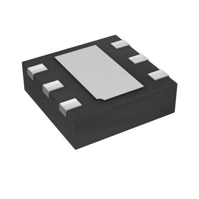
| 供应商器件封装 | 4-WLCSP(0.76x0.76) |
| 其它名称 | FPF1203UCXCT |
| 内部开关 | 是 |
| 包装 | 剪切带 (CT) |
| 安装类型 | 表面贴装 |
| 封装/外壳 | 4-UFBGA,WLCSP |
| 工作温度 | -40°C ~ 85°C |
| 标准包装 | 1 |
| 电压-输入 | 1.2 V ~ 5.5 V |
| 电流限制 | 2.2A |
| 类型 | 高端 |
| 输出数 | 1 |


- 商务部:美国ITC正式对集成电路等产品启动337调查
- 曝三星4nm工艺存在良率问题 高通将骁龙8 Gen1或转产台积电
- 太阳诱电将投资9.5亿元在常州建新厂生产MLCC 预计2023年完工
- 英特尔发布欧洲新工厂建设计划 深化IDM 2.0 战略
- 台积电先进制程称霸业界 有大客户加持明年业绩稳了
- 达到5530亿美元!SIA预计今年全球半导体销售额将创下新高
- 英特尔拟将自动驾驶子公司Mobileye上市 估值或超500亿美元
- 三星加码芯片和SET,合并消费电子和移动部门,撤换高东真等 CEO
- 三星电子宣布重大人事变动 还合并消费电子和移动部门
- 海关总署:前11个月进口集成电路产品价值2.52万亿元 增长14.8%


PDF Datasheet 数据手册内容提取
Is Now Part of To learn more about ON Semiconductor, please visit our website at www.onsemi.com Please note: As part of the Fairchild Semiconductor integration, some of the Fairchild orderable part numbers will need to change in order to meet ON Semiconductor’s system requirements. Since the ON Semiconductor product management systems do not have the ability to manage part nomenclature that utilizes an underscore (_), the underscore (_) in the Fairchild part numbers will be changed to a dash (-). This document may contain device numbers with an underscore (_). Please check the ON Semiconductor website to verify the updated device numbers. The most current and up-to-date ordering information can be found at www.onsemi.com. Please email any questions regarding the system integration to Fairchild_questions@onsemi.com. ON Semiconductor and the ON Semiconductor logo are trademarks of Semiconductor Components Industries, LLC dba ON Semiconductor or its subsidiaries in the United States and/or other countries. ON Semiconductor owns the rights to a number of patents, trademarks, copyrights, trade secrets, and other intellectual property. A listing of ON Semiconductor’s product/patent coverage may be accessed at www.onsemi.com/site/pdf/Patent-Marking.pdf. ON Semiconductor reserves the right to make changes without further notice to any products herein. ON Semiconductor makes no warranty, representation or guarantee regarding the suitability of its products for any particular purpose, nor does ON Semiconductor assume any liability arising out of the application or use of any product or circuit, and specifically disclaims any and all liability, including without limitation special, consequential or incidental damages. Buyer is responsible for its products and applications using ON Semiconductor products, including compliance with all laws, regulations and safety requirements or standards, regardless of any support or applications information provided by ON Semiconductor. “Typical” parameters which may be provided in ON Semiconductor data sheets and/or specifications can and do vary in different applications and actual performance may vary over time. All operating parameters, including “Typicals” must be validated for each customer application by customer’s technical experts. ON Semiconductor does not convey any license under its patent rights nor the rights of others. ON Semiconductor products are not designed, intended, or authorized for use as a critical component in life support systems or any FDA Class 3 medical devices or medical devices with a same or similar classification in a foreign jurisdiction or any devices intended for implantation in the human body. Should Buyer purchase or use ON Semiconductor products for any such unintended or unauthorized application, Buyer shall indemnify and hold ON Semiconductor and its officers, employees, subsidiaries, affiliates, and distributors harmless against all claims, costs, damages, and expenses, and reasonable attorney fees arising out of, directly or indirectly, any claim of personal injury or death associated with such unintended or unauthorized use, even if such claim alleges that ON Semiconductor was negligent regarding the design or manufacture of the part. ON Semiconductor is an Equal Opportunity/Affirmative Action Employer. This literature is subject to all applicable copyright laws and is not for resale in any manner.
F P F 1 2 August 2016 0 3 / F P F FPF1203 / FPF1203L / FPF1204 / FPF12045 1 2 0 IntelliMAX™ Ultra-Small, Slew-Rate-Controlled Load Switch 3 L / F Features Description P F 1 1.2 V to 5.5 V Input Voltage Operating Range The FPF1203 / 03L / 04 / 45 are ultra-small integrated 2 0 Typical R : IntelliMAX™ load switches with integrated P-channel 4 ON switch and analog control features. Integrated slew- / 45 mΩ at VIN=5.5 V rate control prevents inrush current and the resulting F P 55 mΩ at VIN=3.3 V excessive voltage drop on the power rail. The input F voltage range operates from 1.2 V to 5.5 V to provide 1 90 mΩ at VIN=1.8 V 2 power-disconnect capability for post-regulated power 0 185 mΩ at VIN=1.2 V rails in portable and consumer products. The low shut- 4 5 Slew Rate Control with tR: off current allows power designs to meet standby and — off-power drain specifications. FPF1203/FPF1203l/FPF1204: 100 µs I FPF12045: 2 µs The FPF120x are controlled by a logic input (ON pin) nt compatible with standard CMOS GPIO circuitry found e Output Discharge Function on FPF1204 / 45 on Field Programmable Gate Array (FPGA) embedded lli M Low <1.5 µA Quiescent Current processors. The FPF120x are available in 0.76 mm x A ESD Protected: Above 7 kV HBM, 2 kV CDM 0.76 mm 4-bump WLCSP. X ™ GPIO / CMOS-Compatible Enable Circuitry Applications U l t 4-Bump, WLCSP 0.76 mm x 0.76 mm, Mobile Devices and Smart Phones ra 0.4 mm Pitch - S Portable Media Devices m Tablet PCs al l , Advanced Notebook, UMPC, MID S l e Portable Medical Devices w GPS and Navigation Equipment -R a t e - C o n Ordering Information t r o l Switch l Top Output ON Pin e Part Number Mark (Typical) Discharge Activity tR Package d at 3.3V L IN o a FPF1203UCX QL 55 mΩ NA Active HIGH 100 µs d FPF1203LUCX QP 55 mΩ NA Active LOW 100 µs S w FPF1204UCX QM 55 mΩ 65 Ω Active HIGH 100 µs 4-Bump, Wafer-Level Chip- it c FPF1204UCX_F013 Scale Package (WLCSP), h (Amkor Assembly Only) QM 55 mΩ 65 Ω Active HIGH 100 µs 0.76 mm x 0.76 mm, 0.4 mm Pitch FPF1204BUCX QM 55 mΩ 65 Ω Active HIGH 100 µs (Backside Laminate) FPF12045UCX NC 55 mΩ 65 Ω Active HIGH 2 µs © 2011 Fairchild Semiconductor Corporation www.fairchildsemi.com FPF1203 / FPF1203L / FPF1204 / FPF12045 • Rev. 1.14
Application Diagram F P F 1 2 0 VIN VIN VOUT VOUT 3 / F FPF1203/03L/04/45 P F + 1 - CIN ON GND COUT 20 3 L / F P F 1 2 0 4 Figure 1. Typical Application / F P F 1 2 0 Functional Block Diagram 4 5 — I n FPF1203/03L/04/45 t e l VIN VOUT liM A X ™ U l t r a ON CONTROL -S LOGIC m Turn-On Slew Rate a Controlled Driver l l , S R ESD Protection le w Output Discharge - R (Optional) a t e - C o n t r o l l GND e d L Figure 2. Functional Block Diagram (Output Discharge for FPF1204 / 45) o a d S w i t c h © 2011 Fairchild Semiconductor Corporation www.fairchildsemi.com FPF1203 / FPF1203L / FPF1204 / FPF12045 • Rev. 1.14 2
F P F 1 Pin Configurations 2 0 3 / F P F 1 2 0 3 L / F Figure 3. WLCSP Bumps Facing Down Figure 4. WLCSP Bumps Facing Up P (Top View) (Bottom View) F 1 2 0 4 / F VO UT A 1 A 2 VI N VI N A 2 A 1 VO UT PF 1 2 0 4 GN D B 1 B 2 ON ON B 2 B 1 GN D 5 — I n t e Figure 5. Pin Assignments (Top View) Figure 6. Pin Assignments (Bottom View) l l i M A X ™ U Pin Definitions l t r a Pin # Name Description - S m A1 V Switch output OUT a A2 VIN Supply input: input to the power switch ll, S B1 GND Ground l e B2 ON ON/OFF Control, active HIGH; FPF1203/04/45 w - B2 ON ON/OFF Control, active LOW; FPF1203L R a t e - C o n t r o l l e d L o a d S w i t c h © 2011 Fairchild Semiconductor Corporation www.fairchildsemi.com FPF1203 / FPF1203L / FPF1204 / FPF12045 • Rev. 1.14 3
F P Absolute Maximum Ratings F 1 Stresses exceeding the absolute maximum ratings may damage the device. The device may not function or be 2 0 operable above the recommended operating conditions and stressing the parts to these levels is not recommended. 3 In addition, extended exposure to stresses above the recommended operating conditions may affect device reliability. / F The absolute maximum ratings are stress ratings only. P F Symbol Parameter Min. Max. Unit 1 2 0 VIN VIN, VOUT, VON to GND -0.3 6.0 V 3 L ISW Maximum Continuous Switch Current at Ambient Operating Temperature 2.2 A / F P Power Dissipation at T =25°C 1.0 W D A P F T Storage Temperature Range -65 +150 °C STG 1 1S2P with One Thermal Via(1) 110 20 JA Thermal Resistance, Junction-to-Ambient 1S2P without Thermal Via(2) 95 °C/W 4 / F Human Body Model, 7 P JESD22-A114 F ESD Electrostatic Discharge Capability(1,2) kV 1 Charged Device Model, 2 2 0 JESD22-C101 4 5 Notes: — 1. Measured using 2S2P JEDEC std. PCB. 2. Measured using 2S2P JEDEC PCB COLD PLATE Method. I n t e ll i M A Recommended Operating Conditions X ™ The Recommended Operating Conditions table defines the conditions for actual device operation. Recommended U operating conditions are specified to ensure optimal performance to the datasheet specifications. Fairchild does not lt r recommend exceeding them or designing to Absolute Maximum Ratings. a - S Symbol Parameter Min. Max. Unit m a VIN Input Voltage 1.2 5.5 V ll, TA Ambient Operating Temperature -40 +85 °C Sl e w - R a t e - C o n t r o l l e d L o a d S w i t c h © 2011 Fairchild Semiconductor Corporation www.fairchildsemi.com FPF1203 / FPF1203L / FPF1204 / FPF12045 • Rev. 1.14 4
F Electrical Characteristics P F 1 Unless otherwise noted, VIN=1.2 V to 5.5 V and TA=-40 to +85°C. Typical values are at VIN=3.3 V and TA=25°C. 2 0 Symbol Parameter Condition Min. Typ. Max. Unit 3 / Basic Operation F P V Supply Voltage 1.2 5.5 V F IN 1 2 Off Supply FPF1203/04/45 VON=GND, VOUT=Open, VIN=5.5 V 0.1 1.0 0 IQ(OFF) Current FPF1203L VON=VIN, VOUT=Open, VIN=5.5 V 1.0 2.0 μA 3L I Shutdown FPF1203/04/45 VON=GND, VOUT=GND 0.1 1.0 μA / F SD Current FPF1203L V =V , V =GND 1.2 3.0 P ON IN OUT F Quiescent FPF1203/04/45 IOUT=0 mA, VON=VIN, =5.5 V 12 I 0.1 1.5 μA Q Current FPF1203L IOUT=0 mA, VON=GND, VIN, = 5.5 V 04 VIN=5.5 V, IOUT=200 mA, TA=25°C 45 55(3) / F V =3.3 V, I =200 mA, T =25°C 55 65(3) P IN OUT A F R On Resistance V =1.8 V, I =200 mA, T =25°C 90 100(3) mΩ 1 ON IN OUT A 2 VIN=1.2 V, IOUT=200 mA, TA=25°C 185 220(3) 04 5 VIN=1.8 V, IOUT=200 mA, TA=85°C(3) 105 — VIN=3.3 V, VON=OFF, I R Output Discharge R I =20 mA, T =25°C, 65 75 Ω n PD PULL DOWN FORCE A t FPF1204 / FPF12045 e l l i M V On Input Logic HIGH Voltage V =1.2 V to 5.5 V 1.15 V IH IN A X ™ VIL On Input Logic LOW Voltage VIN=1.2 V to 5.5 V 0.65 V U l t r R Pull-Down Resistance at ON Pin V =1.2 V to 5.5 V 8.3 MΩ a ON_PD IN - S ION On Input Leakage VON=VIN or GND 1 μA m Dynamic Characteristics a l l tDON Turn-On Delay(4) 70 , S t V Rise Time(4) 100 le R OUT w tON Turn-On Time(6) VIN=3.3 V, RL=10 Ω, CL=0.1 µF, 170 μs -R tDON Turn-On Delay(4) TA=25°C, FPF12045 2 at tR VOUT Rise Time(4) 2 e-C t Turn-On Time(6) 4 o ON n t Turn-Off Delay(4,5) 0.5 t DOFF r tF VOUT Fall Time(4,5) VTAIN==235.°3C V, ,F RPLF=11200 Ω3L, CL=0.1 µF, 2.0 μs olle t Turn-Off Time(5,7) 2.5 d OFF tDOFF Turn-Off Delay(4,5) 6 Lo V =3.3 V, R =500 Ω, C =0.1 µF, a tF VOUT Fall Time(4,5) TIN=25°C, FPLF1203L L 115 μs d A t Turn-Off Time(5,7) 121 S OFF w t Turn-Off Delay(4,5) 4.0 i DOFF t t V Fall Time(4,5) VIN=3.3 V, RL=10 Ω, CL=0.1 µF, 2.9 μs ch F OUT TA=25°C, FPF1203 t Turn-Off Time(5,7) 7.3 OFF t Turn-Off Delay(4,5) 6 DOFF t V Fall Time(4,5) VIN=3.3 V, RL=500 Ω, CL=0.1 µF, 115 μs F OUT T =25°C, FPF1203 A t Turn-Off Time(5,7) 121 OFF Continued on the following page… © 2011 Fairchild Semiconductor Corporation www.fairchildsemi.com FPF1203 / FPF1203L / FPF1204 / FPF12045 • Rev. 1.14 5
F Electrical Characteristics P F 1 Unless otherwise noted, VIN=1.2 V to 5.5 V and TA=-40 to +85°C. Typical values are at VIN=3.3 V and TA=25°C. 2 0 Symbol Parameter Condition Min. Typ. Max. Unit 3 / t Turn-Off Delay(4,5) 4.0 F DOFF P tF VOUT Fall Time(4,5) VTIN==235.°3C V, ,F RPLF=11200 Ω4/,4 C5L(5=) 0.1 µF, 2.5 μs F1 A t Turn-Off Time(5,7) 6.5 2 OFF 0 tDOFF Turn-Off Delay(4,5) 6 3L tF VOUT Fall Time(4,5) VTIN==235.°3C V, ,F RPLF=1520004Ω/4, 5C(5L)= 0.1 µF, 11 μs / F A t Turn-Off Time(5,7) 17 P OFF F Notes: 1 2 3. This parameter is guaranteed by design and characterization; not production tested. 0 4. t /t /t /t are defined in Figure 23. 4 DON DOFF R F 5. Output discharge enabled during off-state. / F 6. tON=tR + tDON. P 7. t =t + t F OFF F DOFF. 1 2 0 4 5 — I n t e l l i M A X ™ U l t r a - S m a l l , S l e w - R a t e - C o n t r o l l e d L o a d S w i t c h © 2011 Fairchild Semiconductor Corporation www.fairchildsemi.com FPF1203 / FPF1203L / FPF1204 / FPF12045 • Rev. 1.14 6
F Typical Performance Characteristics P F 1 2 0 3 / F P F 1 2 0 3 L / F P F 1 2 0 Figure 7. Shutdown Current vs. Temperature Figure 8. Shutdown Current vs. Supply Voltage 4 / F P F 1 2 0 4 5 — I n t e l l i M A X ™ Figure 9. Off Supply Current vs. Temperature Figure 10. Off Supply Current vs. Supply Voltage U (V Floating) (V Floating) OUT OUT l t r a - S m a l l , S l e w - R a t e - C o n t Figure 11. Quiescent Current vs. Temperature Figure 12. Quiescent Current vs. Supply Voltage r o l l e d L o a d S w i t c h Figure 13. R vs. Temperature Figure 14. R vs. Supply Voltage ON ON © 2011 Fairchild Semiconductor Corporation www.fairchildsemi.com FPF1203 / FPF1203L / FPF1204 / FPF12045 • Rev. 1.14 7
F P F Typical Performance Characteristics (Continued) 1 2 0 3 100 / F P 100µs F A) 10 1 NT ( 1ms 20 E 3 RR L U 1 10ms N C RDS(ON)Limit 100ms / F RAI Single Pulse 1s P I, DD0.1 RqJTAA== 1 2150ooCC/W 1D0Cs F12 0 4 0.01 / F 0.1 1 10 P VDS, DRAIN-SOURCE VOLTAGE (V) F 1 Figure 16. Drain Current vs. Drain-Source Voltage 2 Figure 15. ON Pin Threshold vs. V 0 IN Safe Operating Area 4 5 — I n t e l l i M A X ™ U l t r a - S m a l l , S l e Figure 17. Turn-On Response – FPF1203 / 04 w (VIN=3.3 V, CIN=1 µF, COUT=0.1 µF, RL=10 Ω) -R a t e - C o n t r o l l e d L o a d S w i t c h Figure 18. Turn-Off Response – FPF1203 Figure 19. Turn-Off Response – FPF1203 (V =3.3 V, C =1 µF, C =0.1 µF, R =10 Ω) (V =3.3 V, C =1 µF, C =0.1 µF, R =500 Ω) IN IN OUT L IN IN OUT L © 2011 Fairchild Semiconductor Corporation www.fairchildsemi.com FPF1203 / FPF1203L / FPF1204 / FPF12045 • Rev. 1.14 8
F P F 1 Typical Performance Characteristics (Continued) 2 0 3 / F P F 1 2 0 3 L / F P F 1 2 0 4 / F P F 1 2 0 Figure 20. Turn-Off Response (V =3.3 V, C =1 µF, Figure 21. Turn-Off Response (V =3.3 V, C =1 µF, 4 IN IN IN IN 5 COUT=0.1 µF, RL=10 Ω, FPF1204 / 45) COUT=0.1 µF, RL=500 Ω, FPF1204 / 45) — I n t e l l i M A X ™ U l t r a - S m a l l , S l e w - R a t e - C o n t r o l l e d L o a d S w i t c h © 2011 Fairchild Semiconductor Corporation www.fairchildsemi.com FPF1203 / FPF1203L / FPF1204 / FPF12045 • Rev. 1.14 9
F P F Operation and Application Description 1 2 0 The FPF1203 / 03L / 04 / 045 are low-R P-channel Output Capacitor 3 ON load switches with controlled turn-on. The core of each / device is a 55 m P-channel MOSFET and controller AV 0.1 aµnFd c aGpNaDci toprin, sC.O TUTh,i ss hcoauplda cbiteo rp lparceevde nbtest wpeaerna stihtiec FP capable of functioning over a wide input operating range OUT F board inductance from forcing V below GND when of 1.2 to 5.5 V. OUT 1 the switch is on. C greater than C is highly 2 IN OUT 0 The FPF1204 / 45 contain a 65 on-chip load resistor recommended. COUT greater than CIN can cause VOUT to 3 for quick output discharge when the switch is turned off. exceed VIN when the system supply is removed. This L could result in current flow through the body diode from / The FPF12045 features a faster VOUT Rise Time of 5 μs. VOUT to VIN. FP F 1 VIN VIN VOUT VOUT 20 FPF1204 4 +- CIN OFFON ON GND COUT / F P F 1 2 0 Figure 22. Typical Application 4 5 — I Input Capacitor n t e To limit the voltage drop on the input supply caused by ll transient inrush current when the switch turns on into a iM discharged load capacitor or short-circuit, a capacitor Figure 23. Timing Diagram for FPF1203/4/045 A must be placed between the V and GND pins. A 1 µF X IN ceramic capacitor, C , placed close to the pins is ™ usually sufficient. HigINher-value CIN can be used to Board Layout U l reduce the voltage drop in higher-current applications. t r For best performance, traces should be as short as a - possible. To be most effective, input and output S capacitors should be placed close to the device to m minimize the effect of parasitic trace inductance on a l normal and short-circuit operation. Using wide traces or l, large copper planes for all pins (VIN, VOUT, ON, and S l GND) minimizes the parasitic electrical effects and the e w case-ambient thermal impedance. However, the VOUT - pin should not connect directly to the battery source due R a to the discharge mechanism of the load switch. t e - C o n The table below pertains to the Packaging information on the following page. t r o l Product Dimensions le d D E X Y L o 760 µm ± 30 µm 760 µm ± 30 µm 0.180 mm± 0.018 µm 0.180 mm± 0.018 µm a d S w it c h © 2011 Fairchild Semiconductor Corporation www.fairchildsemi.com FPF1203 / FPF1203L / FPF1204 / FPF12045 • Rev. 1.14 10
F 0.03 C E A 2X B 0.40 Ø0.20 Cu Pad A1 BALL A1 D 0.40 INDEX AREA Ø0.30 0.03 C Solder Mask 2X TOP VIEW RECOMMENDED LAND PATTERN (NSMD PAD TYPE) 0.06 C 0.539 0.292±0.018 0.461 E 0.05 C 0.208±0.021 C SEATING PLANE SIDE VIEWS D NOTES: A. NO JEDEC REGISTRATION APPLIES. B. DIMENSIONS ARE IN MILLIMETERS. 0.005 C A B Ø0.260±0.020 C. DIMENSIONS AND TOLERANCE 0.40 4X PER ASME Y14.5M, 1994. B (Y)±0.018 D. DATUM C IS DEFINED BY THE SPHERICAL 0.40 A CROWNS OF THE BALLS. F 1 2 E. PACKAGE NOMINAL HEIGHT IS 500 MICRONS (X)±0.018 ±39 MICRONS (461-539 MICRONS). F. FOR DIMENSIONS D, E, X, AND Y SEE PRODUCT DATASHEET. BOTTOM VIEW G. DRAWING FILNAME: MKT-UC004AFrev2.
ON Semiconductor and are trademarks of Semiconductor Components Industries, LLC dba ON Semiconductor or its subsidiaries in the United States and/or other countries. ON Semiconductor owns the rights to a number of patents, trademarks, copyrights, trade secrets, and other intellectual property. A listing of ON Semiconductor’s product/patent coverage may be accessed at www.onsemi.com/site/pdf/Patent−Marking.pdf. ON Semiconductor reserves the right to make changes without further notice to any products herein. ON Semiconductor makes no warranty, representation or guarantee regarding the suitability of its products for any particular purpose, nor does ON Semiconductor assume any liability arising out of the application or use of any product or circuit, and specifically disclaims any and all liability, including without limitation special, consequential or incidental damages. Buyer is responsible for its products and applications using ON Semiconductor products, including compliance with all laws, regulations and safety requirements or standards, regardless of any support or applications information provided by ON Semiconductor. “Typical” parameters which may be provided in ON Semiconductor data sheets and/or specifications can and do vary in different applications and actual performance may vary over time. All operating parameters, including “Typicals” must be validated for each customer application by customer’s technical experts. ON Semiconductor does not convey any license under its patent rights nor the rights of others. ON Semiconductor products are not designed, intended, or authorized for use as a critical component in life support systems or any FDA Class 3 medical devices or medical devices with a same or similar classification in a foreign jurisdiction or any devices intended for implantation in the human body. Should Buyer purchase or use ON Semiconductor products for any such unintended or unauthorized application, Buyer shall indemnify and hold ON Semiconductor and its officers, employees, subsidiaries, affiliates, and distributors harmless against all claims, costs, damages, and expenses, and reasonable attorney fees arising out of, directly or indirectly, any claim of personal injury or death associated with such unintended or unauthorized use, even if such claim alleges that ON Semiconductor was negligent regarding the design or manufacture of the part. ON Semiconductor is an Equal Opportunity/Affirmative Action Employer. This literature is subject to all applicable copyright laws and is not for resale in any manner. PUBLICATION ORDERING INFORMATION LITERATURE FULFILLMENT: N. American Technical Support: 800−282−9855 Toll Free ON Semiconductor Website: www.onsemi.com Literature Distribution Center for ON Semiconductor USA/Canada 19521 E. 32nd Pkwy, Aurora, Colorado 80011 USA Europe, Middle East and Africa Technical Support: Order Literature: http://www.onsemi.com/orderlit Phone: 303−675−2175 or 800−344−3860 Toll Free USA/Canada Phone: 421 33 790 2910 Fax: 303−675−2176 or 800−344−3867 Toll Free USA/Canada Japan Customer Focus Center For additional information, please contact your local Email: orderlit@onsemi.com Phone: 81−3−5817−1050 Sales Representative © Semiconductor Components Industries, LLC www.onsemi.com www.onsemi.com 1
Mouser Electronics Authorized Distributor Click to View Pricing, Inventory, Delivery & Lifecycle Information: O N Semiconductor: FPF1203UCX