ICGOO在线商城 > 集成电路(IC) > PMIC - 配电开关,负载驱动器 > TPS22949ADRGR
 Datasheet下载
- 型号: TPS22949ADRGR
- 制造商: Texas Instruments
- 库位|库存: xxxx|xxxx
- 要求:
| 数量阶梯 | 香港交货 | 国内含税 |
| +xxxx | $xxxx | ¥xxxx |
查看当月历史价格
查看今年历史价格
TPS22949ADRGR产品简介:
ICGOO电子元器件商城为您提供TPS22949ADRGR由Texas Instruments设计生产,在icgoo商城现货销售,并且可以通过原厂、代理商等渠道进行代购。 TPS22949ADRGR价格参考¥4.20-¥9.47。Texas InstrumentsTPS22949ADRGR封装/规格:PMIC - 配电开关,负载驱动器, 。您可以下载TPS22949ADRGR参考资料、Datasheet数据手册功能说明书,资料中有TPS22949ADRGR 详细功能的应用电路图电压和使用方法及教程。
TPS22949ADRGR 是由 Texas Instruments(德州仪器)生产的一款 PMIC(电源管理集成电路),属于配电开关和负载驱动器类别。它主要用于需要精确控制电流、电压以及保护电路的应用场景。以下是其主要应用场景:

1. 工业自动化设备
   TPS22949ADRGR 可用于工业控制器、传感器接口、可编程逻辑控制器 (PLC) 和数据采集系统中,提供高效的负载切换和保护功能,确保设备在复杂环境下稳定运行。

2. 通信基础设施
   在基站、路由器、交换机等通信设备中,该芯片可以实现对不同模块的电源分配和管理,支持热插拔功能,减少系统启动时的冲击电流。

3. 消费类电子产品
   适用于笔记本电脑、平板电脑和其他便携式设备中的外围设备供电管理,如 USB 端口、存储卡读卡器等,提供过流、短路和过温保护。

4. 汽车电子系统
   在汽车信息娱乐系统、导航模块和 ADAS(高级驾驶辅助系统)中,TPS22949ADRGR 能够为各种负载提供可靠的电源切换,并具备强大的保护机制以应对恶劣的工作条件。

5. 医疗设备
   用于监护仪、超声波设备和其他便携式或台式医疗仪器中,确保关键组件的安全供电并延长设备寿命。

6. 物联网 (IoT) 设备
   支持智能家居、智能城市和工业物联网设备中的电源管理需求,优化功耗并提高系统的可靠性和耐用性。

TPS22949ADRGR 的特性使其非常适合需要高精度电流限制、快速响应时间和多种保护功能的应用场合。通过集成这些功能,它可以简化设计流程,降低整体系统成本,同时提升产品的性能和安全性。
| 参数 | 数值 |
| 产品目录 | 集成电路 (IC) |
| 描述 | IC LOAD SWITCH LN LDO 8SON |
| 产品分类 | PMIC - 电源分配开关 |
| 品牌 | Texas Instruments |
| 数据手册 | |
| 产品图片 |
|
| 产品型号 | TPS22949ADRGR |
| Rds(On) | 400 毫欧 |
| rohs | 无铅 / 符合限制有害物质指令(RoHS)规范要求 |
| 产品系列 | - |
| 产品目录页面 | |
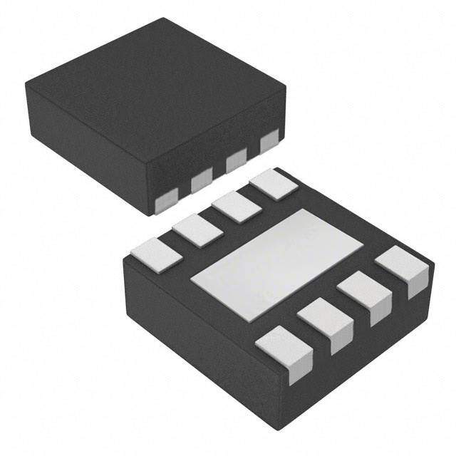
| 供应商器件封装 | 8-SON(3x3) |
| 其它名称 | 296-25317-6 |
| 内部开关 | 是 |
| 包装 | Digi-Reel® |
| 安装类型 | 表面贴装 |
| 封装/外壳 | 8-WFDFN 裸露焊盘 |
| 工作温度 | -40°C ~ 85°C |
| 开关类型 | 通用 |
| 标准包装 | 1 |
| 比率-输入:输出 | 1:1 |
| 特性 | 自动重启,负载释放 |
| 电压-负载 | 1.62 V ~ 4.5 V |
| 电压-输入 | 1.62 V ~ 4.5 V |
| 电流-输出(最大值) | 100mA |
| 电流限制 | 150mA |
| 类型 | 通用 |
| 输入类型 | 非反相 |
| 输出数 | 2 |
| 输出类型 | P 通道 |


- 商务部:美国ITC正式对集成电路等产品启动337调查
- 曝三星4nm工艺存在良率问题 高通将骁龙8 Gen1或转产台积电
- 太阳诱电将投资9.5亿元在常州建新厂生产MLCC 预计2023年完工
- 英特尔发布欧洲新工厂建设计划 深化IDM 2.0 战略
- 台积电先进制程称霸业界 有大客户加持明年业绩稳了
- 达到5530亿美元!SIA预计今年全球半导体销售额将创下新高
- 英特尔拟将自动驾驶子公司Mobileye上市 估值或超500亿美元
- 三星加码芯片和SET,合并消费电子和移动部门,撤换高东真等 CEO
- 三星电子宣布重大人事变动 还合并消费电子和移动部门
- 海关总署:前11个月进口集成电路产品价值2.52万亿元 增长14.8%


PDF Datasheet 数据手册内容提取
Product Sample & Technical Tools & Support & Folder Buy Documents Software Community TPS22949,TPS22949A SLVS908D–FEBRUARY2009–REVISEDJUNE2015 TPS22949x Current-Limited Load Switch With Low Noise Regulation Capability 1 Features 3 Description • IntegratedCurrentLimiter The TPS22949 and TPS22949A are devices that 1 provide protection to systems and loads in high- – InputVoltageRange:1.62Vto4.5V current conditions. The device contains a 500-mΩ – LowON-Resistance current-limited P-channel MOSFET that can operate – r =300-mΩ atV =4.5V over an input voltage range of 1.62 V to 4.5 V as well ON IN as a low-dropout (LDO) regulator with a fixed output – r =350-mΩ atV =3.3V ON IN voltageof1.8V. – r =400-mΩ atV =2.5V ON IN The switch is controlled by an on/off input (EN1), – r =600-mΩ atV =1.8V ON IN which can interface directly with low-voltage control – Integrated100-mAMinimumCurrentLimit signals. When the switch current reaches the – UndervoltageLockout maximum limit, the TPS22949/TPS22949A operates in a constant-current mode to prohibit excessive – Fast-CurrentLimitResponseTime currents from causing damage. If the constant current – IntegratedFaultBlankingandAutoRestart condition persists after 12 ms, these devices shut off • StableWithoutCurrentLimiterOutputCapacitor the switch and pull the fault signal pin (OC) low. The (TPS22949AOnly) TPS22949/TPS22949A has an auto-restart feature that turns the switch on again after 70 ms if the EN1 • IntegratedLow-NoiseRFLDO pinisstillactive. – InputVoltageRange:1.62Vto4.5V The output of the current limiter is internally – LowNoise:50 μVrms(10Hzto100kHz) connected to an RF low-dropout (LDO) regulator that – 80-dBV PSRR(10Hzto10kHz) offers good AC performance with very low ground IN – FastStart-UpTime:130 μs current, good power supply rejection ratio (PSRR), low noise, fast start-up, and excellent line and load – LowDropout100mVatI =100mA load transient response. The output of the regulator is – IntegratedOutputDischarge stable with ceramic capacitors. This LDO uses a – StableWith2.2-μFOutputCapacitor precision voltage reference and feedback loop to achieve overall accuracy of 2% over all load, line, • 1.8-VCompatibleControlInputThreshold process,andtemperaturevariations. • ESDPerformanceTestedPerJESD22 – 3500VHumanBodyModel DeviceInformation(1) (A114-B,ClassII) PARTNUMBER PACKAGE BODYSIZE(NOM) – 1000VChargedDeviceModel TPS22949 DSBGA(8) 1.90mm×0.90mm (C101) DSBGA(8) 1.90mm×0.90mm TPS22949A • Tiny8-TerminalYZPPackage(1.9mm ×0.9mm, WSON(8) 3.00mm×3.00mm 0.5-mmPitch,0.5-mmHeight)andWSON-8 (DRG)3.0mm×3.0mm (1) For all available packages, see the orderable addendum at theendofthedatasheet. 2 Applications TypicalApplicationSchematic • FingerprintModuleProtection TPS22949 TPS22949A • PortableConsumerElectronics VIN VIN VOUTCL VOUTCL • SmartPhones EN1 CIN CCL • Notebooks EN2 • ControlAccessSystems V+ V+ VOUTLDO V(1O.8UVT,L D10O0 mA) CLDO GND OC OC RPU 1 An IMPORTANT NOTICE at the end of this data sheet addresses availability, warranty, changes, use in safety-critical applications, intellectualpropertymattersandotherimportantdisclaimers.PRODUCTIONDATA.
TPS22949,TPS22949A SLVS908D–FEBRUARY2009–REVISEDJUNE2015 www.ti.com Table of Contents 1 Features.................................................................. 1 8.2 FunctionalBlockDiagram.......................................15 2 Applications........................................................... 1 8.3 FeatureDescription.................................................16 3 Description............................................................. 1 8.4 DeviceFunctionalModes........................................17 4 RevisionHistory..................................................... 2 9 ApplicationandImplementation........................ 18 9.1 ApplicationInformation............................................18 5 Description(continued)......................................... 3 9.2 TypicalApplication .................................................19 6 PinConfigurationandFunctions......................... 4 9.3 SystemExamples...................................................21 7 Specifications......................................................... 5 10 PowerSupplyRecommendations..................... 22 7.1 AbsoluteMaximumRatings......................................5 11 Layout................................................................... 22 7.2 ESDRatings..............................................................5 11.1 LayoutGuidelines.................................................22 7.3 RecommendedOperatingConditions.......................5 11.2 LayoutExample....................................................22 7.4 ThermalInformation..................................................5 12 DeviceandDocumentationSupport................. 23 7.5 ElectricalCharacteristics...........................................6 7.6 CurrentLimiterElectricalCharacteristics..................6 12.1 RelatedLinks........................................................23 7.7 Low-NoiseLDORegulatorElectricalCharacteristics7 12.2 CommunityResources..........................................23 7.8 CurrentLimiterSwitchingCharacteristics.................7 12.3 Trademarks...........................................................23 7.9 TypicalCharacteristics..............................................8 12.4 ElectrostaticDischargeCaution............................23 12.5 Glossary................................................................23 8 DetailedDescription............................................ 15 13 Mechanical,Packaging,andOrderable 8.1 Overview.................................................................15 Information........................................................... 23 4 Revision History ChangesfromRevisionC(January2010)toRevisionD Page • AddedESDRatingstable,FeatureDescriptionsection,DeviceFunctionalModes,ApplicationandImplementation section,PowerSupplyRecommendationssection,Layoutsection,DeviceandDocumentationSupportsection,and Mechanical,Packaging,andOrderableInformationsection.................................................................................................. 1 • DeletedDissipationRatingstable........................................................................................................................................... 5 2 SubmitDocumentationFeedback Copyright©2009–2015,TexasInstrumentsIncorporated ProductFolderLinks:TPS22949 TPS22949A
TPS22949,TPS22949A www.ti.com SLVS908D–FEBRUARY2009–REVISEDJUNE2015 5 Description (continued) The TPS22949A integrates additional internal circuitry that increases the current limit of the switch during the power-up sequence. This feature allows the TPS22949A to operate without a storage capacitor at the input of theLDO. The TPS22949 and TPS22949A are available in a space-saving 8-terminal WCSP (YZP) or in an 8-pin WSON package (DRG). Both devices are characterized for operation over the free-air temperature range of –40°C to 85°C. Copyright©2009–2015,TexasInstrumentsIncorporated SubmitDocumentationFeedback 3 ProductFolderLinks:TPS22949 TPS22949A
TPS22949,TPS22949A SLVS908D–FEBRUARY2009–REVISEDJUNE2015 www.ti.com 6 Pin Configuration and Functions YZPPackage 8-PinDSBGA TopView D D C C B B A A 2 1 1 2 Laser MarkingView BumpView DRGPackage 8-PinWSON TopView EN2 1 8 V+ Exposed GND 2 Thermal 7 VOUTLDO Die Pad VIN 3 on 6 VOUTCL Underside EN1 4 5 OC Theexposedcenterpad,ifused,mustbeconnectedasasecondaryGNDorleftelectricallyopen. PinFunctions PIN I/O DESCRIPTION NAME DSBGA WSON EN1 D2 4 I Powerswitchcontrolinput.Activehigh.Donotleavefloating. EN2 A2 1 I LDOcontrolinput.Activehigh.Donotleavefloating. GND B2 2 — Ground Overcurrentoutputflag.Activelow,open-drainoutputthatindicatesanovercurrent,supply OC D1 5 O undervoltage,orovertemperaturestate. V A1 8 I Supplyvoltage + V C2 3 I Supplyinput.Inputtothepowerswitch;bypassthisinputwithaceramiccapacitortoground. IN V C1 6 O Switchoutput.Outputofthepowerswitch OUTCL V B1 7 O LDOoutput.OutputoftheRFLDOfixedto1.8V(1). OUTLDO (1) Outputvoltagesfrom0.9Vto3.6Vin50-mVincrementsareavailablethroughtheuseofinnovativefactoryEEPROMprogramming; minimumorderquantitiesmayapply.Contactfactoryfordetailsandavailability. YZPPackagePinAssignments D EN1 OC C V V IN OUTCL B GND V OUTLDO A EN2 V + 2 1 4 SubmitDocumentationFeedback Copyright©2009–2015,TexasInstrumentsIncorporated ProductFolderLinks:TPS22949 TPS22949A
TPS22949,TPS22949A www.ti.com SLVS908D–FEBRUARY2009–REVISEDJUNE2015 7 Specifications 7.1 Absolute Maximum Ratings(1) MIN MAX UNIT V Inputvoltage V ,EN1,EN2,V –0.3 6 V I IN + V Currentlimiteroutputvoltage V +0.3 V OUTCL IN T Operatingjunctiontemperature –40 105 °C J T Storagetemperature –65 150 °C stg (1) StressesbeyondthoselistedunderAbsoluteMaximumRatingsmaycausepermanentdamagetothedevice.Thesearestressratings only,whichdonotimplyfunctionaloperationofthedeviceattheseoranyotherconditionsbeyondthoseindicatedunderRecommended OperatingConditions.Exposuretoabsolute-maximum-ratedconditionsforextendedperiodsmayaffectdevicereliability. 7.2 ESD Ratings VALUE UNIT Humanbodymodel(HBM),perANSI/ESDA/JEDECJS-001(1) ±3500 V(ESD) Electrostaticdischarge Chargeddevicemodel(CDM),perJEDECspecificationJESD22- ±1000 V C101(2) (1) JEDECdocumentJEP155statesthat500-VHBMallowssafemanufacturingwithastandardESDcontrolprocess. (2) JEDECdocumentJEP157statesthat250-VCDMallowssafemanufacturingwithastandardESDcontrolprocess. 7.3 Recommended Operating Conditions MIN NOM MAX UNIT V Inputvoltage(1) 1.62 4.5 V IN V Currentlimiteroutputvoltage V V OUTCL IN V Supplyvoltage 2.6 5.5 V + C Inputcapacitor 1 μF IN T Ambientfree-airtemperature –40 85 °C A CONTROLINPUTS(EN1,EN2) V High-levelinputvoltage 1.4 5.5 V IH V Low-levelinputvoltage 0.4 V IL (1) SeetheApplicationandImplementation. 7.4 Thermal Information TPS22949x THERMALMETRIC(1) YZP[DSBGA] DRG[WSON] UNIT 8PINS 8PINS R Junction-to-ambientthermalresistance 105.8 51.3 °C/W θJA R Junction-to-case(top)thermalresistance 1.6 65.4 °C/W θJC(top) R Junction-to-boardthermalresistance 10.8 25.9 °C/W θJB ψ Junction-to-topcharacterizationparameter 3.1 1.3 °C/W JT ψ Junction-to-boardcharacterizationparameter 10.8 26 °C/W JB R Junction-to-case(bottom)thermalresistance N/A 6.1 °C/W θJC(bot) (1) Formoreinformationabouttraditionalandnewthermalmetrics,seetheSemiconductorandICPackageThermalMetricsapplication report,SPRA953. Copyright©2009–2015,TexasInstrumentsIncorporated SubmitDocumentationFeedback 5 ProductFolderLinks:TPS22949 TPS22949A
TPS22949,TPS22949A SLVS908D–FEBRUARY2009–REVISEDJUNE2015 www.ti.com 7.5 Electrical Characteristics T =–40°Cto85°C(unlessotherwisenoted) A PARAMETER TESTCONDITIONS MIN TYP(1) MAX UNIT EN1andEN2=V + V =V +1.4Vor2.5,whichever>5.5V, I Groundpincurrent + OUT 85 110 μA GND V ≥V +0.5V OUTCL OUTLDO I =0mA OUT2 Groundpincurrent(current I EN1=V andEN2=0 40 75 μA GNDCL limiteronly) + EN1andEN2=GND, V =V =3.3V 2 IN + I OFF-stategroundpincurrent V =Open, μA GND(OFF) OUTCL VOUTLDO=Open VIN=3.6V,V+=5.5V 6 I Enablepin2current,enabled VEN2=V =5.5V,V =4.5V 1 μA EN2 + IN I Enablepin1current,enabled VEN1=V =5.5V,V =4.5V 1 μA EN1 + IN TPS22949 122 Shutdownthreshold(T ) A TPS22949A 135 Thermal TPS22949 112 Returnfromshutdown °C shutdown TPS22949A 120 TPS22949 10 Hysteresis TPS22949A 10 (1) TypicalvaluesareatV =3.3VandT =25°C. IN A 7.6 Current Limiter Electrical Characteristics overoperatingfree-airtemperaturerange,V =3.3V,EN1=V ,EN2=GND(unlessotherwisenoted) + + YZPPACKAGE DRGPACKAGE PARAMETER TESTCONDITIONS T UNIT A MIN TYP MAX MIN TYP MAX 25°C 0.3 0.4 0.4 0.5 V =4.5V IN Full 0.5 0.6 25°C 0.35 0.6 0.45 0.7 V =3.3V IN Full 0.7 0.8 25°C 0.4 0.7 0.5 0.8 r ON-stateresistance I =20mA V =2.5V Ω ON OUT IN Full 0.8 0.9 25°C 0.6 0.9 0.7 1 V =1.8V IN Full 1.0 1.1 V =1.62 25°C 0.7 1.0 0.8 1.1 IN V Full 1.1 1.2 I Currentlimit V =3V V =3.3V Full 100 150 200 100 150 200 LIM OUT IN Power-ONinrush mA I currentlimit V =3V V =3.3V Full 750 750 LIM(INRUSH) OUT IN (TPS22949Aonly) Undervoltage UVLO-CL V increasing 1.39 1.49 1.59 1.39 1.49 1.59 V shutdown IN Undervoltage 30 30 mV shutdownhysteresis OCoutputlogiclow VIN=4.5V 0.1 0.3 0.1 0.3 I =10mA Full V voltage SINK V =1.8V 0.2 0.4 0.2 0.4 IN 6 SubmitDocumentationFeedback Copyright©2009–2015,TexasInstrumentsIncorporated ProductFolderLinks:TPS22949 TPS22949A
TPS22949,TPS22949A www.ti.com SLVS908D–FEBRUARY2009–REVISEDJUNE2015 7.7 Low-Noise LDO Regulator Electrical Characteristics overoperatingfree-airtemperaturerange(unlessotherwisenoted) PARAMETER TESTCONDITIONS MIN TYP MAX UNIT V Outputvoltage(1) 1.76 1.8 1.84 V OUTLDO V lineregulation V =V +0.5Vto4.5V,I =1mA ±0.1 %/V IN IN OUTLDO OUT ΔV /ΔV OUTLDO IN V linetransient ΔV =400mV,t =t =1μs ±2 mV IN IN r f V =V +1.4Vor2.5V,whicheveris>5.5V, V lineregulation IN OUTLDO ±0.1 %/V ΔVOUTLDO/ΔV+ + IOUT=1mA V linetransient ΔV =600mV,t =t =1μs ±5 mV + IN r f Loadregulation I =0to100mA(noloadtofullload) ±0.01 %/V OUT2 ΔV /ΔI OUTLDO OUT2 Loadtransient I =0to100mA,t =t =1μs ±35 mV OUT2 r f Dropoutvoltage V =V –0.1V,V –V =1.4V, V IN OUTLDO(NOM) + OUTLDO(NOM) 110 200 mV DO (V =V –V ) I =100mA DO IN OUTLDO OUT f=10Hz 75 f=100Hz 75 Powersupply VOUTCL–VOUTLDO≥0.5V, f=1kHz 80 V PSRR V =V +1.4V, dB IN rejectionratio I + =O1U0T0LDmOA, f=10kHz 80 OUT f=100kHz 85 f=1MHz 85 f=10Hz 80 f=100Hz 80 Powersupply VOUTCL–VOUTLDO≥0.5V, f=1kHz 75 V PSRR V =V +1.4V, dB + rejectionratio I + =O1U0T0LDmOA, f=10kHz 65 OUT f=100kHz 55 f=1MHz 35 V ≥2.5V, V Outputnoisevoltage + BW=10Hzto100kHz 50 μVrms N V =V +0.5V OUTLDO OUTCL V =95%, t Start-uptime OUT 130 250 μs STR V ,I =100mA,C =2.2μF OUT(NOM) OUT OUT Undervoltagelockout V rising 2.3 2.45 2.55 V + UVLO-V + Hysteresis V falling 150 mV + (1) LDOoutputvoltageisfixedat1.8V.However,outputvoltagesfrom0.9Vto3.6Vin50-mVincrementsareavailablethroughtheuseof innovativefactoryEEPROMprogramming;minimumorderquantitiesmayapply.Contactfactoryfordetailsandavailability. 7.8 Current Limiter Switching Characteristics V =3.3V,T =25°C,R =500Ω,C =0.1μF(unlessotherwisenoted) IN A L L PARAMETER TESTCONDITIONS MIN TYP MAX UNIT t Turnontime R =500Ω,C =0.1μF 95 μs ON L CL t Turnofftime R =500Ω,C =0.1μF 2 μs OFF L CL t V risetime R =500Ω,C =0.1μF 25 μs r OUT L CL t V falltime R =500Ω,C =0.1μF 10 μs f OUT L CL t Overcurrentblankingtime 6 12 18 ms BLANK t Auto-restarttime 40 80 120 ms RSTRT Power-ONinrushcurrentlimittime t R =500Ω,C =0.1μF 150 μs INRUSH (TPS22949Aonly) L CL V =V =3.3V,moderateovercurrentcondition 11 IN EN1 Short-circuitresponsetime μs V =V =3.3V,hardshort 5 IN EN1 Copyright©2009–2015,TexasInstrumentsIncorporated SubmitDocumentationFeedback 7 ProductFolderLinks:TPS22949 TPS22949A
TPS22949,TPS22949A SLVS908D–FEBRUARY2009–REVISEDJUNE2015 www.ti.com 7.9 Typical Characteristics 0.9 0.9 V+= 2.5V 0.8 V+= 3.3V 0.8 W() V+= 4.5V W() N N e, rO0.7 e, rO0.7 nc nc a a esist 0.6 esist 0.6 R R e e Stat 0.5 Stat 0.5 VIN= 1.8V ON- ON- VIN= 3.6V 0.4 0.4 VIN= 4.5V VIN= 5V 0.3 0.3 1.5 2.5 3.5 4.5 5.5 –40 –10 25 55 85 InputVoltage,VIN(V) Temperature,TA(°C) T =25°C V =5.5V A + Figure1.ON-StateResistancevsInputVoltage Figure2.ON-StateResistancevsTemperature, –85 –30 –86 –50 –87 –88 –70 A) –89 A) m m ( ( D –90 D–90 N N G G I –91 I –110 –92 –93 –130 –94 –95 –150 2.0 2.5 3.0 3.5 4.0 4.5 5.0 2.2 2.4 2.6 2.8 3.0 3.2 3.4 InputVoltage,VIN(V) InputVoltage,VIN(V) V =5.5V V =3.3V + + Figure3.GroundPinCurrentvsInputVoltage Figure4.GroundPinCurrentvsInputVoltage –80 -38.0 –85 -38.5 -39.0 –90 -39.5 –95 A) A) m m -40.0 (D–100 (D N N IG VIN= 3.3V IG -40.5 –105 VIN= 4.5V -41.0 –110 -41.5 –115 -42.0 –120 -42.5 –40 –10 25 55 85 1.5 2.0 2.5 3.0 3.5 4.0 4.5 5.0 Temperature,TA(°C) InputVoltage,VIN(V) V =5.5V V =5.5V + + Figure5.GroundPinCurrentvsTemperature Figure6.GroundPinCurrentvsInputVoltage (CurrentLimiterOnly) 8 SubmitDocumentationFeedback Copyright©2009–2015,TexasInstrumentsIncorporated ProductFolderLinks:TPS22949 TPS22949A
TPS22949,TPS22949A www.ti.com SLVS908D–FEBRUARY2009–REVISEDJUNE2015 Typical Characteristics (continued) 0 -3.00 -5 VIN= 1.8V -3.05 -10 VIN= 3.3V -3.10 VIN= 4.5V -15 -3.15 A)m -20 (nA) -3.20 I(GND --3205 ND(OFF)--33..3205 G -35 I -3.35 -40 -3.40 -45 -3.45 -50 -3.50 –40 –10 25 55 85 1.5 2.0 2.5 3.0 3.5 4.0 4.5 5.0 Temperature,TA(°C) InputVoltage,VIN(V) V+=5.5V V+=5.5V Figure7.GroundPinCurrentvsTemperature Figure8.OFF-StateGroundCurrentvsInputVoltage (CurrentLimiterOnly) 0 0 -100 -0.5 VIN= 3.6V V = 4.5V -200 IN -1.0 -300 A) -1.5 (n -400 A) OFF) -500 (mF) -2.0 GND( -600 D(OF -2.5 I N G -3.0 -700 I -3.5 -800 -900 -4.0 -1000 -4.5 2.0 2.5 3.0 3.5 4.0 4.5 5.0 5.5 6.0 –40 –10 25 55 85 InputVoltage,VIN(V) Temperature,TA(°C) V =V IN + Figure9.OFF-StateGroundCurrentvsInputVoltage Figure10.OFF-StateGroundCurrentvsTemperature 1.800 0.18 T = –40°C 1.795 V) 0.16 TAA= –10°C (V)O111...777889050 IIIOOOUUUTTT=== 011 0mm0AA mA Voltage,V(LDO000...111024 TTTAAA=== 258555°°°CCC LD out 0.08 T p VOU1.775 O Dro 0.06 1.770 LD 0.04 1.765 0.02 1.760 0.00 –40 –10 25 55 85 -0.10 -0.09 -0.08 -0.07 -0.06 -0.05 -0.04 -0.03 -0.02 -0.01 0.00 Temperature,TA(°C) LDO Output Current,IOUTLDO(A) Figure11.OutputVoltagevsTemperature Figure12.LDODropoutVoltagevsOutputCurrent Copyright©2009–2015,TexasInstrumentsIncorporated SubmitDocumentationFeedback 9 ProductFolderLinks:TPS22949 TPS22949A
TPS22949,TPS22949A SLVS908D–FEBRUARY2009–REVISEDJUNE2015 www.ti.com Typical Characteristics (continued) 1.797 1.82 1.796 1.80 1.795 (V) (V) 1.78 O O UTLD1.794 TTAA== ––4100°°CC UTLD VO TA= 25°C VO 1.76 1.793 TA= 55°C TA= 85°C TTAA== ––4100°°CC 1.792 1.74 TTAA== 2555°°CC TA= 85°C 1.791 1.72 2.0 2.5 3.0 3.5 4.0 4.5 5.0 2.0 2.5 3.0 3.5 4.0 4.5 5.0 InputVoltage,VIN(V) InputVoltage,VIN(V) IOUT=0mA IOUT=100mA Figure13. InputVoltage,VIN,LineRegulation Figure14. InputVoltage,VIN,LineRegulation 1.797 1.779 1.796 1.778 1.795 V) V)1.777 ( ( O O LD1.794 TA= –40°C LD VOUT TTAA== –2150°C°C VOUT1.776 TTAA== ––4100°°CC 1.793 TA= 55°C TA= 25°C TA= 85°C TA= 55°C 1.775 TA= 85°C 1.792 1.791 1.774 3.0 3.5 4.0 4.5 5.0 5.5 6.0 3.0 3.5 4.0 4.5 5.0 5.5 6.0 InputVoltage,V+(V) InputVoltage,V+(V) I =0mA I =100mA OUT OUT Figure15. InputVoltage,V ,LineRegulation Figure16.InputVoltage,V ,LineRegulation + + 1.800 1.797 1.796 1.795 1.795 1.790 V) V) ( (1.794 TLDO1.785 TLDO TTAA== ––4100°°CC OU TA= –40°C OU1.793 TA= 25°C V T = –10°C V TA= 55°C 1.780 A TA= 85°C T = 25°C 1.792 A T = 55°C A 1.775 TA= 85°C 1.791 1.770 1.790 -0.10 -0.09 -0.08 -0.07 -0.06 -0.05 -0.04 -0.03 -0.02 -0.01 0.00 -0.10 -0.09 -0.08 -0.07 -0.06 -0.05 -0.04 -0.03 -0.02 -0.01 0.00 I (A) I (A) OUTLDO OUTLDO I =100mA I =10mA OUT OUT Figure17.LoadRegulation Figure18.LoadRegulationUnderLightLoads 10 SubmitDocumentationFeedback Copyright©2009–2015,TexasInstrumentsIncorporated ProductFolderLinks:TPS22949 TPS22949A
TPS22949,TPS22949A www.ti.com SLVS908D–FEBRUARY2009–REVISEDJUNE2015 Typical Characteristics (continued) e e s s n n o o p p s s e e R R ut ut p p ut ut O O DO DIV DO DIV LV/ LV/ al,m al,m nt Sign50 LLoDaOd OTuratpnusti eRnet sSpigonnasel nt Sign50 Load Transient Signal e e nsi nsi LDO Output Response a a Tr Tr d d a a o o L L 100µs/DIV 100µs/DIV Figure19.LoadTransient Figure20.V LoadTransient IN 1.41E-6 z) H T1.21E-6 R 1 mV/div ms/ Vr1.01E-6 ( y DO ensit810E-9 L D VIN VVIONU=T 2=. 11.V8 tVo 2.5V VOUT Noise 610E-9 V = 3.2V al IO+UTLDO= 100 mA pectr410E-9 S 200 mV/div put 210E-9 ut O 10E-9 100 1000 10000 100000 100µs/DIV Frequency (Hz) Figure21.V+LoadTransient Figure22.OutputSpectralNoiseDensityvsFrequency 0 -10 IOUTLDO= 0 mA -10 IOUTLDO= 1 mA IOUTLDO= 50 mA -20 IOUTLDO= 100 mA -30 IOUTLDO= 100 mA -30 B) -50 -40 d R R ( SR-50 R P S P -70 -60 -70 -90 -80 -90 -110 10 100 1000 10000 100000 1000000 -100 0 10 100 1000 10000 100000 1000000 Frequency (Hz) Frequency (Hz) Figure23.PSRRvsFrequency Figure24.V PSRRvsFrequency + Copyright©2009–2015,TexasInstrumentsIncorporated SubmitDocumentationFeedback 11 ProductFolderLinks:TPS22949 TPS22949A
TPS22949,TPS22949A SLVS908D–FEBRUARY2009–REVISEDJUNE2015 www.ti.com Typical Characteristics (continued) 180 80 T fall 160 70 T ON 140 60 s) 120 (µF µs)50 CL= 0.1 µF t/tONOF 18000 CILLO=A D0.1= µ1F0, mRAL= 330Ω t/t(risefall40 IRLLOA=D 33=0 1Ω0 mA 60 V =V = 3.3V 30 IN + 40 20 TOFF Trise 20 10 -50 -25 0 25 50 75 100 -50 -25 0 25 50 75 100 Temperature (°C) Temperature (°C) Figure25.tON/tOFFvsTemperature Figure26.trise/tfallvsTemperature 5.5 2.0 5.0 1.8 Vin=1.8V- 4.5 Vin=2.5V- 1.6 4.0 Vin=3.0V- 1.4 Vin=3.3V- 3.5 Vin=4.5V- 1.2 Vout(V) 223...050 Vin=5.0V- LDO_out(V) 01..80 VV++==23.V5-V- V+=3.3V- 0.6 1.5 V+=3.6V- 1.0 0.4 V+=4.5V- V+=5V- 0.5 0.2 V+=5.5V- 0.0 0.0 -0.5 -0.2 0.0 0.5 1.0 1.5 2.0 0.0 0.5 1.0 1.5 2.0 InputVoltage,EN1(V) InputVoltage,EN2(V) V+=5.5V VIN=3.3V Figure27.EN1(CurrentLimiter)InputThresholds Figure28.EN2(LDO)InputThresholds V (*) DRV V (A) DRV 2V/DIV 2V/DIV V OUTCL V OUTCL 2V/DIV 2V/DIV I OUTCL I 100 mA/DIV OUTCL 100mA/DIV V OC 2V/DIV V OC 2V/DIV 2 ms/DIV 20 ms/DIV VDRVsignalforcesthedevicetogointoovercurrentmode. VDRVsignalforcesthedevicetogointoovercurrentmode. Figure29.tBLANKResponse Figure30.tRESTARTResponse 12 SubmitDocumentationFeedback Copyright©2009–2015,TexasInstrumentsIncorporated ProductFolderLinks:TPS22949 TPS22949A
TPS22949,TPS22949A www.ti.com SLVS908D–FEBRUARY2009–REVISEDJUNE2015 Typical Characteristics (continued) C = 0.1uF OUTCL IOUTCL 1mA/DIV I R = 500-W OUTCL OUTCL 1 mA/DIV VIN= 3.3V C = 0.1uF OUTCL R = 500-! OUTCL V = 3.3-V IN V EN1 1V/DIV V 1V/DIV EN1 50uS/DIV 50 us/DIV Figure31.CurrentLimitertONResponse Figure32.CurrentLimitertOFFResponse V V IN IN 2V/DIV 2V/DIV C = 10uF IN C = 1uF I OUTCL OUTCL 400mA/DIV I OUTLDO 400mA/DIV V OUTLDO 2V/DIV V OUTCL 2V/DIV 10uS/DIV 10uS/DIV Figure33.Short-CircuitResponseTime Figure34.Short-CircuitResponseTime (V ShortedtoGND) (V ShortedtoGND) OUTCL OUTLDO V /V IN EN2 1V/DIV V /V IN EN1 1V/DIV I1O0U0TCmLA/DIV CCIN= 10=u 1FuF OUTCL I OUTLDO 100mA/DIV 20uS/DIV 20uS/DIV Figure35.Short-CircuitResponseTime(SwitchPowerUp Figure36. Short-CircuitResponseTime(LDOPowerUpto toHardShort)(TPS22949) HardShort)(TPS22949) Copyright©2009–2015,TexasInstrumentsIncorporated SubmitDocumentationFeedback 13 ProductFolderLinks:TPS22949 TPS22949A
TPS22949,TPS22949A SLVS908D–FEBRUARY2009–REVISEDJUNE2015 www.ti.com Typical Characteristics (continued) C = 10uF IN C = 1uF OUTCL V IN 1V/DIV V IN 1V/DIV I OUTCL I 200mA/DIV OUTLDO 200mA/DIV C = 10uF C = 10uF IN IN COUTCL= 0.1uF COUTCL= 0.1uF 20uS/DIV 20uS/DIV Figure37.Short-CircuitResponseTime(SwitchPowerUp Figure38.Short-CircuitResponseTime(LDOPowerUpto toHardShort)(TPS22949A) HardShort)(TPS22949A) V V IN IN 2V/DIV 2V/DIV C = 10uF IN V C = 1uF EN2 OUTCL 2V/DIV V EN1 2V/DIV I OUTCL 100mA/DIV IOUTLDO 100mA/DIV V OUTCL (Shorted to VOUTLDO Ground) (Shorted to Ground) 20uS/DIV 20uS/DIV Figure39.CurrentLimitResponseTime(CurrentLimiter) Figure40.CurrentLimitResponseTime(LDO) 14 SubmitDocumentationFeedback Copyright©2009–2015,TexasInstrumentsIncorporated ProductFolderLinks:TPS22949 TPS22949A
TPS22949,TPS22949A www.ti.com SLVS908D–FEBRUARY2009–REVISEDJUNE2015 8 Detailed Description 8.1 Overview The TPS22949 and TPS22949A are devices that provide protection to systems and loads in high-current conditions. The device contains a 500-mΩ current-limited P-channel MOSFET that can operate over an input voltage range of 1.62 V to 4.5 V. In addition, these devices feature a low-dropout regulator (LDO) with a fixed output voltage of 1.8 V. When the switch current reaches the maximum limit, the TPS22949/TPS22949A operates in a constant-current mode to prohibit excessive currents from causing damage. The fault signal pin (OC) will signal the constant current condition if it persists after 12 ms. The output of the current limiter is internallyconnectedtotheLDO. 8.2 Functional Block Diagram V , Supply bias + (2.5V to 5.5V) OC, Over-current flag V , Current limiter input Current Limiter IN (1.62V to 4.5V) with VOUTCL, Current limiter output Auto-Restart Feature EN1, Active high V , LDO output Low-Noise LDO OUTLDO (Fixed, 1.8V max, 100 mA) EN2, Active high GND Figure41. SimplifiedBlockDiagram Copyright©2009–2015,TexasInstrumentsIncorporated SubmitDocumentationFeedback 15 ProductFolderLinks:TPS22949 TPS22949A
TPS22949,TPS22949A SLVS908D–FEBRUARY2009–REVISEDJUNE2015 www.ti.com Functional Block Diagram (continued) C2 (3) V IN UVLO + – D2 (4) Current EN1 Limit Control A2 (1) EN2 Logic C1 (6) V OUTCL UVLO A1 (8) V + + Bandgap – B1 (7) V OUTLDO e g ar h c s di ut p out D1 (5) Thermal OC Shutdown GND Figure42. DetailedBlockDiagram 8.3 Feature Description 8.3.1 UndervoltageLockout(UVLO) The undervoltage lockout turns off the switch if the input voltage drops below the undervoltage lockout threshold. With the ON pin active, the input voltage rising above the undervoltage lockout threshold causes a controlled turnon of the switch, which limits current overshoots. The TPS22949 and TPS22949A also have a UVLO on the V biasvoltageandkeeptheoutputoftheLDOshutoffuntiltheinternalcircuitryisoperatingproperly. + 8.3.2 FaultReporting Whenanovercurrent,inputundervoltage,orovertemperatureconditionisdetected,OCissetactivelowtosignal the fault mode. OC is an open-drain MOSFET and requires a pullup resistor between V and OC. During IN shutdown,thepulldownonOCisdisabled,thusreducingcurrentdrawfromthesupply. 8.3.3 CurrentLimiting When the switch current reaches the maximum limit, the TPS22949/TPS22949A operates in a constant-current mode to prohibit excessive currents from causing damage. TPS22949/TPS22949A has a minimum current limit of100mA. 16 SubmitDocumentationFeedback Copyright©2009–2015,TexasInstrumentsIncorporated ProductFolderLinks:TPS22949 TPS22949A
TPS22949,TPS22949A www.ti.com SLVS908D–FEBRUARY2009–REVISEDJUNE2015 8.4 Device Functional Modes Table1summarizestheLDOstateasdeterminedbytheEN1andEN2pins. Table1.FunctionTable STATEOFTHEDEVICE EN1 EN2 CurrentlimiterandLDOdisabled 0 X CurrentlimiterenabledandLDOdisabled 1 0 CurrentlimiterandLDOenabled 1 1 Copyright©2009–2015,TexasInstrumentsIncorporated SubmitDocumentationFeedback 17 ProductFolderLinks:TPS22949 TPS22949A
TPS22949,TPS22949A SLVS908D–FEBRUARY2009–REVISEDJUNE2015 www.ti.com 9 Application and Implementation NOTE Information in the following applications sections is not part of the TI component specification, and TI does not warrant its accuracy or completeness. TI’s customers are responsible for determining suitability of components for their purposes. Customers should validateandtesttheirdesignimplementationtoconfirmsystemfunctionality. 9.1 Application Information This application illustrates the TPS22949 and TPS22949A configured with a 100-mA sinking load with both enablestiedtothesameinputvoltage. 9.1.1 InputVoltage Theinputvoltage(V )ofthecurrentlimiterissetfrom1.62Vto4.5V,howeverifboththecurrentlimiterandthe IN LDO are enabled, the user must be careful to keep the input voltage (V ) greater than 1.8 V + (voltage drop IN through the switch) + (voltage drop through the LDO); otherwise, the LDO does not have a high enough internal inputsignaltooperateproperly. A current limiter input voltage ramp time less than the blanking time (approximately 10 ms typical) is recommended. If the ramp time extends beyond the blanking period, then the current limiter goes into recycle, andthesystemmaynotstartoroperateproperly. 9.1.2 Input/OutputCapacitors Although an input capacitor is not required for stability of on the input pin (V ), it is good analog design practice IN to connect a 0.1-μF to 1-μF low equivalent series resistance (ESR) capacitor across the IN pin input supply near the regulator. This capacitor counteracts reactive input sources and improves transient response, noise rejection, and ripple rejection. A higher value capacitor may be necessary if large, fast rise time load transients are anticipated, or if the device is located close to the power source. If source impedance is not sufficiently low, a 0.1-μF input capacitor may be necessary to ensure stability. The V bias pin does not require an input capacitor + because it does not source high currents. However, if source impedance is not sufficiently low, a small 0.1-μF bypasscapacitorisrecommended. A 0.1-μF capacitor C , must be placed between V and GND. This capacitor prevents parasitic board CL OUTCL inductancesfromforcingV belowGNDwhentheswitchturnsoff. OUTCL 18 SubmitDocumentationFeedback Copyright©2009–2015,TexasInstrumentsIncorporated ProductFolderLinks:TPS22949 TPS22949A
TPS22949,TPS22949A www.ti.com SLVS908D–FEBRUARY2009–REVISEDJUNE2015 9.2 Typical Application TPS22949 TPS22949A V V V V IN IN OUTCL OUTCL EN1 C C IN CL EN2 V+ V+ V VOUTLDO OUTLDO (1.8V, 100 mA) C LDO GND OC OC R PU Figure43. TPS22949/TPS22949ATypicalApplicationWithBothEnablePinsTiedtotheInputVoltage 9.2.1 DesignRequirements Forthisdesignexample,usetheparameterslistedinTable2astheinputparameters. Table2.DesignParameters DESIGNPARAMETER EXAMPLEVALUE V 3.3V IN V+ 3.3V C 4.7µF IN C 2.2µF LDO 9.2.2 DetailedDesignProcedure 9.2.2.1 Start-UpSequence For the TPS22949, the total output capacitance must be kept below a maximum value, C , to prevent the CL(max) part from registering an overcurrent condition and turning off the switch. The maximum output capacitance can bedeterminedfromEquation1: C =I ×t ÷V (1) CL LIM(MAX) BLANK(MIN) IN DuetotheintegralbodydiodeinthePMOSswitch,aC greaterthanC ishighlyrecommended.AC greater IN CL CL than C can cause V to exceed V when the system supply is removed. This could result in current flow IN OUTCL IN throughthebodydiodefromV toV . OUTCL IN On TPS22949, a storage capacitor (C ) at the output of the current limiter is recommended to provide enough CL currenttotheLDOduringthestart-upsequence.Thestoragecapacitorisneededtoreducetheamountofinrush current supplied through the current-limited load switch to the LDO during the power-up sequence (see Figure44).IftheC capacitoristoosmall,theinrushcurrentneededtostarttheLDOandchargeC couldbe CL LDO interpreted by the current limiter as an overcurrent and, therefore, trigger the current-limiting feature of the switch. The switch would then try to limit the current to the 100-mA limit, and the user would see an undesired droponthesupplyline(seeFigure45). Copyright©2009–2015,TexasInstrumentsIncorporated SubmitDocumentationFeedback 19 ProductFolderLinks:TPS22949 TPS22949A
TPS22949,TPS22949A SLVS908D–FEBRUARY2009–REVISEDJUNE2015 www.ti.com On TPS22949A, the storage capacitor (C ) is not required. TPS22949A integrates an additional internal circuitry CL that increases the current limit of the switch to approximately 750 mA (that is, I ) for about 250 μs (that LIM(INRUSH) is, t ), initiated when the internal circuitry of the LDO is operating properly (that is, when the UVLO of the INRUSH LDO bias (V ) is disabled (V > 2.6 V). Because the current limit is increased during the power-up sequence, a + + potential inrush current through the LDO is not interpreted by the current limiter as an overcurrent. The current neededbytheLDOisthenbesuppliedbytheinputcapacitor(C )ofthecurrentlimiter(seeFigure45). IN TheTPS22949LDO(V )isdesignedtobestablewithstandardceramiccapacitorswithvaluesof2.2μFor OUTLDO larger at the output. X5R- and X7R-type capacitors are best because they have minimal variation in value and ESR over temperature. Maximum ESR must be less than 250 mΩ. Figure 43, Figure 44, and Figure 45 illustrate the behavior of the TPS22949 and TPS22949A with a 100-mA sinking load and different capacitor values for a typicalapplicationwherebothenablesaretiedtothesameinputvoltage(seeFigure43). 9.2.3 ApplicationCurves 3.5 3.5 3.0 3.0 VIN VOUTCL VLDO VIN VOUTCL VLDO 2.5 2.5 V)2.0 ge( (V)2.0 a e olt1.5 ag V VIN=V+=VEN1=VEN2 = 3.3V Volt1.5 VIN=V+=VEN1=VEN2 = 3.3V 1.0 CIN= 4.7 mF, CCL= 2.2 mF CIN= 4.7 mF, CCL= 0 mF CLDO= 2.2mF 1.0 CLDO= 2.2mF 0.5 0.5 0.0 0 0.0005 0.001 0.0015 0.002 0.0025 0.0 Time (s) 0 0.0005 0.001 0.0015 0.002 0.0025 Time (s) Figure44.TPS22949Power-UpSequence Figure45.TPS22949Power-UpSequence 3.5 3.0 VIN VOUTCL VLDO 2.5 2.0 ) V ( e g 1.5 a olt VIN=V+=VEN1=VEN2 = 3.3V V 1.0 CIN= 4.7 mF, CCL= 0 mF C = 2.2mF LDO 0.5 0.0 -0.5 0 0.0005 0.001 0.0015 0.002 0.0025 Time(s) Figure46.TPS22949APower-UpSequence 20 SubmitDocumentationFeedback Copyright©2009–2015,TexasInstrumentsIncorporated ProductFolderLinks:TPS22949 TPS22949A
TPS22949,TPS22949A www.ti.com SLVS908D–FEBRUARY2009–REVISEDJUNE2015 9.3 System Examples V V V V IN IN OUTCL OUTCL EN1 CIN= 4.7µF CCL= 4.7µF EN2 V V + + V V OUTLDO OUTLDO TPS22949 CLDO= 2.2µF GND OC OC R PU Figure47. TPS22949TypicalApplicationSchematic V V V V IN IN OUTCL OUTCL EN1 CIN= 4.7µF CCL= 0.1µF EN2 V V + + V V OUTLDO OUTLDO TPS22949A CLDO= 2.2µF GND OC OC R PU Figure48. TPS22949ATypicalApplicationSchematic Copyright©2009–2015,TexasInstrumentsIncorporated SubmitDocumentationFeedback 21 ProductFolderLinks:TPS22949 TPS22949A
TPS22949,TPS22949A SLVS908D–FEBRUARY2009–REVISEDJUNE2015 www.ti.com 10 Power Supply Recommendations The device is designed to operate from a V+ range of 2.6 V to 5.5 V and VIN range of 1.62 V to 4.5 V (without using the LDO) or >1.8 V to 4.5 V (when using the LDO). This supply must be placed as close to the device pin as possible with the recommended input bypass capacitor. If the supply is located more than a few inches from the device pins, additional bulk capacitance may be required in addition to the ceramic bypass capacitors. If additionalbulkcapacitanceisrequired,anelectrolytic,tantalum,orceramiccapacitorof10 μFmaybesufficient. 11 Layout 11.1 Layout Guidelines For best performance, all traces must be as short as possible. To be most effective, the input and output capacitors must be placed close to the device to minimize the effects that parasitic trace inductances may have on normal operation. Using wide traces for VIN, V+, VOUTLDO, VOUTCL, and GND helps minimize the parasitic electricaleffectsalongwithminimizingthecasetoambientthermalimpedance. 11.2 Layout Example VIA to Power Plane VIA to GND V+ EN2 V GND OUTLDO V VIN OUTCL OC EN1 Exposed Thermal Pad Area Figure49. LayoutSchematic 22 SubmitDocumentationFeedback Copyright©2009–2015,TexasInstrumentsIncorporated ProductFolderLinks:TPS22949 TPS22949A
TPS22949,TPS22949A www.ti.com SLVS908D–FEBRUARY2009–REVISEDJUNE2015 12 Device and Documentation Support 12.1 Related Links The table below lists quick access links. Categories include technical documents, support and community resources,toolsandsoftware,andquickaccesstosampleorbuy. Table3.RelatedLinks TECHNICAL TOOLS& SUPPORT& PARTS PRODUCTFOLDER SAMPLE&BUY DOCUMENTS SOFTWARE COMMUNITY TPS22949 Clickhere Clickhere Clickhere Clickhere Clickhere TPS22949A Clickhere Clickhere Clickhere Clickhere Clickhere 12.2 Community Resources The following links connect to TI community resources. Linked contents are provided "AS IS" by the respective contributors. They do not constitute TI specifications and do not necessarily reflect TI's views; see TI's Terms of Use. TIE2E™OnlineCommunity TI'sEngineer-to-Engineer(E2E)Community.Createdtofostercollaboration amongengineers.Ate2e.ti.com,youcanaskquestions,shareknowledge,exploreideasandhelp solveproblemswithfellowengineers. DesignSupport TI'sDesignSupport QuicklyfindhelpfulE2Eforumsalongwithdesignsupporttoolsand contactinformationfortechnicalsupport. 12.3 Trademarks E2EisatrademarkofTexasInstruments. Allothertrademarksarethepropertyoftheirrespectiveowners. 12.4 Electrostatic Discharge Caution Thesedeviceshavelimitedbuilt-inESDprotection.Theleadsshouldbeshortedtogetherorthedeviceplacedinconductivefoam duringstorageorhandlingtopreventelectrostaticdamagetotheMOSgates. 12.5 Glossary SLYZ022—TIGlossary. Thisglossarylistsandexplainsterms,acronyms,anddefinitions. 13 Mechanical, Packaging, and Orderable Information The following pages include mechanical, packaging, and orderable information. This information is the most current data available for the designated devices. This data is subject to change without notice and revision of thisdocument.Forbrowser-basedversionsofthisdatasheet,refertotheleft-handnavigation. Copyright©2009–2015,TexasInstrumentsIncorporated SubmitDocumentationFeedback 23 ProductFolderLinks:TPS22949 TPS22949A
PACKAGE OPTION ADDENDUM www.ti.com 6-Feb-2020 PACKAGING INFORMATION Orderable Device Status Package Type Package Pins Package Eco Plan Lead/Ball Finish MSL Peak Temp Op Temp (°C) Device Marking Samples (1) Drawing Qty (2) (6) (3) (4/5) TPS22949ADRGR ACTIVE SON DRG 8 3000 Green (RoHS NIPDAU Level-2-260C-1 YEAR -40 to 85 ZUG & no Sb/Br) TPS22949AYZPR ACTIVE DSBGA YZP 8 3000 Green (RoHS SNAGCU Level-1-260C-UNLIM -40 to 85 (4Z, 4Z2) & no Sb/Br) TPS22949YZPR ACTIVE DSBGA YZP 8 3000 Green (RoHS SNAGCU Level-1-260C-UNLIM -40 to 85 (4Y, 4Y2) & no Sb/Br) (1) The marketing status values are defined as follows: ACTIVE: Product device recommended for new designs. LIFEBUY: TI has announced that the device will be discontinued, and a lifetime-buy period is in effect. NRND: Not recommended for new designs. Device is in production to support existing customers, but TI does not recommend using this part in a new design. PREVIEW: Device has been announced but is not in production. Samples may or may not be available. OBSOLETE: TI has discontinued the production of the device. (2) RoHS: TI defines "RoHS" to mean semiconductor products that are compliant with the current EU RoHS requirements for all 10 RoHS substances, including the requirement that RoHS substance do not exceed 0.1% by weight in homogeneous materials. Where designed to be soldered at high temperatures, "RoHS" products are suitable for use in specified lead-free processes. TI may reference these types of products as "Pb-Free". RoHS Exempt: TI defines "RoHS Exempt" to mean products that contain lead but are compliant with EU RoHS pursuant to a specific EU RoHS exemption. Green: TI defines "Green" to mean the content of Chlorine (Cl) and Bromine (Br) based flame retardants meet JS709B low halogen requirements of <=1000ppm threshold. Antimony trioxide based flame retardants must also meet the <=1000ppm threshold requirement. (3) MSL, Peak Temp. - The Moisture Sensitivity Level rating according to the JEDEC industry standard classifications, and peak solder temperature. (4) There may be additional marking, which relates to the logo, the lot trace code information, or the environmental category on the device. (5) Multiple Device Markings will be inside parentheses. Only one Device Marking contained in parentheses and separated by a "~" will appear on a device. If a line is indented then it is a continuation of the previous line and the two combined represent the entire Device Marking for that device. (6) Lead/Ball Finish - Orderable Devices may have multiple material finish options. Finish options are separated by a vertical ruled line. Lead/Ball Finish values may wrap to two lines if the finish value exceeds the maximum column width. Important Information and Disclaimer:The information provided on this page represents TI's knowledge and belief as of the date that it is provided. TI bases its knowledge and belief on information provided by third parties, and makes no representation or warranty as to the accuracy of such information. Efforts are underway to better integrate information from third parties. TI has taken and continues to take reasonable steps to provide representative and accurate information but may not have conducted destructive testing or chemical analysis on incoming materials and chemicals. TI and TI suppliers consider certain information to be proprietary, and thus CAS numbers and other limited information may not be available for release. Addendum-Page 1
PACKAGE OPTION ADDENDUM www.ti.com 6-Feb-2020 In no event shall TI's liability arising out of such information exceed the total purchase price of the TI part(s) at issue in this document sold by TI to Customer on an annual basis. Addendum-Page 2
PACKAGE MATERIALS INFORMATION www.ti.com 18-Jan-2020 TAPE AND REEL INFORMATION *Alldimensionsarenominal Device Package Package Pins SPQ Reel Reel A0 B0 K0 P1 W Pin1 Type Drawing Diameter Width (mm) (mm) (mm) (mm) (mm) Quadrant (mm) W1(mm) TPS22949ADRGR SON DRG 8 3000 330.0 12.4 3.3 3.3 1.1 8.0 12.0 Q2 TPS22949AYZPR DSBGA YZP 8 3000 178.0 9.2 1.02 2.02 0.63 4.0 8.0 Q1 TPS22949YZPR DSBGA YZP 8 3000 178.0 9.2 1.02 2.02 0.63 4.0 8.0 Q1 PackMaterials-Page1
PACKAGE MATERIALS INFORMATION www.ti.com 18-Jan-2020 *Alldimensionsarenominal Device PackageType PackageDrawing Pins SPQ Length(mm) Width(mm) Height(mm) TPS22949ADRGR SON DRG 8 3000 367.0 367.0 35.0 TPS22949AYZPR DSBGA YZP 8 3000 220.0 220.0 35.0 TPS22949YZPR DSBGA YZP 8 3000 220.0 220.0 35.0 PackMaterials-Page2
None
PACKAGE OUTLINE DRG0008A WSON - 0.8 mm max height SCALE 5.000 PLASTIC SMALL OUTLINE - NO LEAD 3.1 B A 2.9 3.1 PIN 1 INDEX AREA 2.9 0.8 0.7 C SEATING PLANE 0.05 0.00 0.08 C (0.2) TYP EXPOSED 1.2 0.1 THERMAL PAD 4 5 2X 1.5 2 0.1 8 1 6X 0.5 0.3 8X 0.2 PIN 1 ID 0.6 8X 0.1 C A B 0.4 0.08 C 4218885/A 03/2020 NOTES: 1. All linear dimensions are in millimeters. Any dimensions in parenthesis are for reference only. Dimensioning and tolerancing per ASME Y14.5M. 2. This drawing is subject to change without notice. 3. The package thermal pad must be soldered to the printed circuit board for thermal and mechanical performance. www.ti.com
EXAMPLE BOARD LAYOUT DRG0008A WSON - 0.8 mm max height PLASTIC SMALL OUTLINE - NO LEAD (1.2) 8X (0.7) SYMM 1 8 8X (0.25) SYMM (2) (0.75) 6X (0.5) 4 5 (R0.05) TYP ( 0.2) VIA (0.35) TYP (2.7) LAND PATTERN EXAMPLE EXPOSED METAL SHOWN SCALE:20X 0.07 MAX 0.07 MIN ALL AROUND ALL AROUND EXPOSED EXPOSED METAL METAL SOLDER MASK METAL METAL UNDER SOLDER MASK OPENING SOLDER MASK OPENING NON SOLDER MASK SOLDER MASK DEFINED DEFINED (PREFERRED) SOLDER MASK DETAILS 4218885/A 03/2020 NOTES: (continued) 4. This package is designed to be soldered to a thermal pad on the board. For more information, see Texas Instruments literature number SLUA271 (www.ti.com/lit/slua271). 5. Vias are optional depending on application, refer to device data sheet. If any vias are implemented, refer to their locations shown on this view. It is recommended that vias under paste be filled, plugged or tented. www.ti.com
EXAMPLE STENCIL DESIGN DRG0008A WSON - 0.8 mm max height PLASTIC SMALL OUTLINE - NO LEAD SYMM 8X (0.7) METAL TYP 8X (0.25) 1 8 SYMM (1.79) 6X (0.5) 4 5 (R0.05) TYP (1.13) (2.7) SOLDER PASTE EXAMPLE BASED ON 0.125 mm THICK STENCIL EXPOSED PAD 84% PRINTED SOLDER COVERAGE BY AREA SCALE:25X 4218885/A 03/2020 NOTES: (continued) 6. Laser cutting apertures with trapezoidal walls and rounded corners may offer better paste release. IPC-7525 may have alternate design recommendations. www.ti.com
PACKAGE OUTLINE YZP0008 DSBGA - 0.5 mm max height SCALE 8.000 DIE SIZE BALL GRID ARRAY B E A BALL A1 CORNER D C 0.5 MAX SEATING PLANE 0.19 0.05 C 0.15 BALL TYP 0.5 TYP D C SYMM 1.5 D: Max = 1.918 mm, Min =1 .858 mm TYP B E: Max = 0.918 mm, Min =0 .858 mm 0.5 TYP A 0.25 8X 1 2 0.21 0.015 C A B SYMM 4223082/A 07/2016 NOTES: 1. All linear dimensions are in millimeters. Any dimensions in parenthesis are for reference only. Dimensioning and tolerancing per ASME Y14.5M. 2. This drawing is subject to change without notice. www.ti.com
EXAMPLE BOARD LAYOUT YZP0008 DSBGA - 0.5 mm max height DIE SIZE BALL GRID ARRAY (0.5) TYP 8X ( 0.23) 1 2 A (0.5) TYP B SYMM C D SYMM LAND PATTERN EXAMPLE SCALE:40X SOLDER MASK 0.05 MAX 0.05 MIN ( 0.23) OPENING SOLDER MASK OPENING ( 0.23) METAL METAL UNDER SOLDER MASK NON-SOLDER MASK SOLDER MASK DEFINED DEFINED (PREFERRED) SOLDER MASK DETAILS NOT TO SCALE 4223082/A 07/2016 NOTES: (continued) 3. Final dimensions may vary due to manufacturing tolerance considerations and also routing constraints. For more information, see Texas Instruments literature number SNVA009 (www.ti.com/lit/snva009). www.ti.com
EXAMPLE STENCIL DESIGN YZP0008 DSBGA - 0.5 mm max height DIE SIZE BALL GRID ARRAY (0.5) TYP 8X ( 0.25) (R0.05) TYP 1 2 A (0.5) TYP B SYMM C METAL TYP D SYMM SOLDER PASTE EXAMPLE BASED ON 0.1 mm THICK STENCIL SCALE:40X 4223082/A 07/2016 NOTES: (continued) 4. Laser cutting apertures with trapezoidal walls and rounded corners may offer better paste release. www.ti.com
IMPORTANTNOTICEANDDISCLAIMER TI PROVIDES TECHNICAL AND RELIABILITY DATA (INCLUDING DATASHEETS), DESIGN RESOURCES (INCLUDING REFERENCE DESIGNS), APPLICATION OR OTHER DESIGN ADVICE, WEB TOOLS, SAFETY INFORMATION, AND OTHER RESOURCES “AS IS” AND WITH ALL FAULTS, AND DISCLAIMS ALL WARRANTIES, EXPRESS AND IMPLIED, INCLUDING WITHOUT LIMITATION ANY IMPLIED WARRANTIES OF MERCHANTABILITY, FITNESS FOR A PARTICULAR PURPOSE OR NON-INFRINGEMENT OF THIRD PARTY INTELLECTUAL PROPERTY RIGHTS. These resources are intended for skilled developers designing with TI products. You are solely responsible for (1) selecting the appropriate TI products for your application, (2) designing, validating and testing your application, and (3) ensuring your application meets applicable standards, and any other safety, security, or other requirements. These resources are subject to change without notice. TI grants you permission to use these resources only for development of an application that uses the TI products described in the resource. Other reproduction and display of these resources is prohibited. No license is granted to any other TI intellectual property right or to any third party intellectual property right. TI disclaims responsibility for, and you will fully indemnify TI and its representatives against, any claims, damages, costs, losses, and liabilities arising out of your use of these resources. TI’s products are provided subject to TI’s Terms of Sale (www.ti.com/legal/termsofsale.html) or other applicable terms available either on ti.com or provided in conjunction with such TI products. TI’s provision of these resources does not expand or otherwise alter TI’s applicable warranties or warranty disclaimers for TI products. Mailing Address: Texas Instruments, Post Office Box 655303, Dallas, Texas 75265 Copyright © 2020, Texas Instruments Incorporated