
 Datasheet下载
- 型号: FM31L278-G
- 制造商: Cypress Semiconductor
- 库位|库存: xxxx|xxxx
- 要求:
| 数量阶梯 | 香港交货 | 国内含税 |
| +xxxx | $xxxx | ¥xxxx |
查看当月历史价格
查看今年历史价格
FM31L278-G产品简介:
ICGOO电子元器件商城为您提供FM31L278-G由Cypress Semiconductor设计生产,在icgoo商城现货销售,并且可以通过原厂、代理商等渠道进行代购。 FM31L278-G价格参考。Cypress SemiconductorFM31L278-G封装/规格:专用 IC, Processor Companion IC Processor-Based Systems 14-SOIC。您可以下载FM31L278-G参考资料、Datasheet数据手册功能说明书,资料中有FM31L278-G 详细功能的应用电路图电压和使用方法及教程。
Cypress Semiconductor Corp(赛普拉斯半导体公司)的专用IC型号FM31L278-G,是一款基于FRAM(铁电随机存取存储器)技术的实时时钟(RTC)芯片。其主要应用场景包括但不限于以下领域:

 1. 数据记录与日志保存
   - FM31L278-G内置FRAM存储器,能够提供高可靠性和快速写入能力,适用于需要频繁记录数据的应用场景,例如环境监测设备、工业传感器、医疗设备等。
   - 在这些设备中,它可以保存时间戳、运行状态、错误日志等关键信息,即使在断电情况下也能确保数据不丢失。

 2. 嵌入式系统时钟管理
   - 作为一款实时时钟芯片,FM31L278-G可以为嵌入式系统提供精确的时间基准,广泛应用于家用电器、工业控制设备、安防监控系统等。
   - 其低功耗特性使其非常适合电池供电的设备,如便携式仪器、智能仪表和手持终端。

 3. 消费电子设备
   - 在消费电子产品中,如数码相机、打印机、扫描仪等,该芯片可用于记录设备使用时间、打印任务时间戳或拍摄照片的时间信息。
   - 它还能帮助设备在重启后快速恢复到之前的状态,提升用户体验。

 4. 工业自动化与控制
   - 工业自动化领域需要高可靠性的时钟和存储解决方案,FM31L278-G的FRAM技术能够在恶劣环境下保持稳定运行。
   - 它可以用于PLC(可编程逻辑控制器)、HMI(人机界面)和其他工业设备中,以记录操作历史和维护计划。

 5. 汽车电子
   - 在汽车行业中,这款芯片可用于车载信息系统、导航设备、黑匣子(行车记录仪)等。
   - 它能记录车辆行驶数据、事故时间点以及诊断信息,为后续分析提供支持。

 6. 医疗设备
   - 医疗设备对数据完整性和可靠性要求极高,FM31L278-G的非易失性存储功能和精确时钟特性非常适用。
   - 可用于心率监测仪、血糖仪、输液泵等设备,记录患者数据和设备运行时间。

 总结
FM31L278-G凭借其FRAM技术和实时时钟功能,适合需要高可靠性、低功耗和快速写入能力的应用场景。无论是消费电子、工业控制还是汽车电子领域,它都能提供精准的时间基准和安全的数据存储解决方案。
| 参数 | 数值 |
| 产品目录 | 集成电路 (IC)半导体 |
| 描述 | IC MEMORY 14SOIC监控电路 256K w/RTC Pwr Mon WDT Bat Sw PF |
| 产品分类 | |
| 品牌 | Cypress Semiconductor Corp |
| 产品手册 | http://www.cypress.com/?docID=42549 |
| 产品图片 |
|
| rohs | 符合RoHS无铅 / 符合限制有害物质指令(RoHS)规范要求 |
| 产品系列 | 电源管理 IC,监控电路,Cypress Semiconductor FM31L278-G- |
| NumberofInputsMonitored | 2 Input |
| 数据手册 | http://www.cypress.com/?docID=42549 |
| 产品型号 | FM31L278-G |
| PCN组件/产地 | http://www.cypress.com/?docID=48502 |
| PCN设计/规格 | http://www.cypress.com/?docID=45719http://www.cypress.com/?docID=47856点击此处下载产品Datasheet |
| 产品种类 | 监控电路 |
| 人工复位 | Manual Reset |
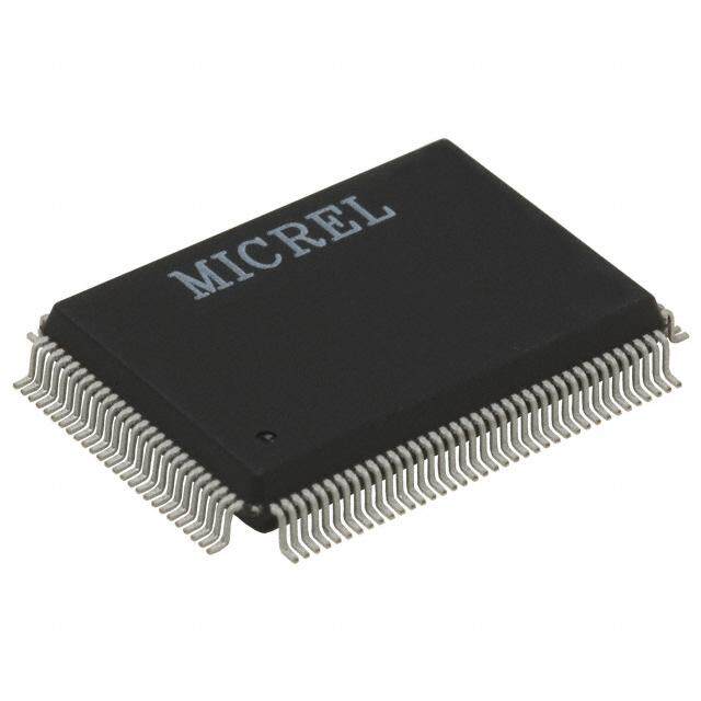
| 供应商器件封装 | 14-SOIC |
| 其它名称 | 428-3222 |
| 功率失效检测 | Yes |
| 包装 | 管件 |
| 商标 | Cypress Semiconductor |
| 安装类型 | 表面贴装 |
| 安装风格 | SMD/SMT |
| 封装 | Tube |
| 封装/外壳 | 14-SOIC(0.154",3.90mm 宽) |
| 封装/箱体 | SOIC-14 |
| 工作电源电流 | 1500 uA |
| 工厂包装数量 | 56 |
| 应用 | 基于处理器的系统 |
| 最大工作温度 | + 85 C |
| 最小工作温度 | - 40 C |
| 标准包装 | 56 |
| 欠电压阈值 | 2.6 V |
| 电池备用开关 | Backup |
| 电源电压-最大 | 3.6 V |
| 电源电压-最小 | 2.7 V |
| 监视器 | Watchdog |
| 类型 | 处理器辅助元件 |
| 系列 | FM31L278-G |
| 被监测输入数 | 2 Input |
| 输出类型 | Active Low, Bidirectional |
| 过电压阈值 | 2.9 V |
| 阈值电压 | 2.6 V, 2.9 V |


- 商务部:美国ITC正式对集成电路等产品启动337调查
- 曝三星4nm工艺存在良率问题 高通将骁龙8 Gen1或转产台积电
- 太阳诱电将投资9.5亿元在常州建新厂生产MLCC 预计2023年完工
- 英特尔发布欧洲新工厂建设计划 深化IDM 2.0 战略
- 台积电先进制程称霸业界 有大客户加持明年业绩稳了
- 达到5530亿美元!SIA预计今年全球半导体销售额将创下新高
- 英特尔拟将自动驾驶子公司Mobileye上市 估值或超500亿美元
- 三星加码芯片和SET,合并消费电子和移动部门,撤换高东真等 CEO
- 三星电子宣布重大人事变动 还合并消费电子和移动部门
- 海关总署:前11个月进口集成电路产品价值2.52万亿元 增长14.8%


PDF Datasheet 数据手册内容提取
FM31L276/FM31L278 64-Kbit/256-Kbit Integrated Processor Companion with F-RAM 64-Kbit/256-Kbit Integrated Processor Companion with F-RAM Features ■Restriction of hazardous substances (RoHS) compliant ■Underwriters laboratory (UL) recognized ■64-Kbit/256-Kbit ferroelectric random access memory (F-RAM) ❐Logically organized as 8K × 8 (FM31L276)/ Functional Description 32K × 8 (FM31L278) ❐High-endurance 100 trillion (1014) read/writes The FM31L276/FM31L278 device integrates F-RAM memory ❐151-year data retention (See Data Retention and Endurance with the most commonly needed functions for processor-based on page 29) systems. Major features include nonvolatile memory, real time ❐NoDelay™ writes clock, low-V reset, watchdog timer, nonvolatile event counter, DD ❐Advanced high-reliability ferroelectric process lockable 64-bit serial number area, and general purpose comparator that can be used for a power-fail (NMI) interrupt or ■High Integration Device Replaces Multiple Parts any other purpose. ❐Serial nonvolatile memory ❐Real time clock (RTC) The FM31L276/FM31L278 is a 64-Kbit/256-Kbit nonvolatile memory employing an advanced ferroelectric process. A ❐Low voltage reset ferroelectric random access memory or F-RAM is nonvolatile ❐Watchdog timer and performs reads and writes similar to a RAM. This memory is ❐Early power-fail warning/NMI truly nonvolatile rather than battery backed. It provides reliable ❐Two 16-bit event counter data retention for 151 years while eliminating the complexities, ❐Serial number with write-lock for security overhead, and system-level reliability problems caused by other ■Real-time Clock/Calendar nonvolatile memories. The FM31L276/FM31L278 is capable of ❐Backup current at 2 V: 1.15 A at +25 C supporting 1014 read/write cycles, or 100 million times more write ❐Seconds through centuries in BCD format cycles than EEPROM. ❐Tracks leap years through 2099 The real time clock (RTC) provides time and date information in ❐Uses standard 32.768 kHz crystal (6 pF/12.5 pF) BCD format. It can be permanently powered from an external ❐Software calibration backup voltage source, either a battery or a capacitor. The ❐Supports battery or capacitor backup timekeeper uses a common external 32.768 kHz crystal and ■Processor Companion provides a calibration mode that allows software adjustment of ❐Active-low reset output for V and watchdog timekeeping accuracy. DD ❐Programmable low-VDD reset trip point The processor companion includes commonly needed CPU ❐Manual reset filtered and debounced support functions. Supervisory functions include a reset output ❐Programmable watchdog timer signal controlled by either a low V condition or a watchdog DD ❐Dual Battery-backed event counter tracks system intrusions timeout. RST goes active when V drops below a DD or other events programmable threshold and remains active for 100 ms after ❐Comparator for power-fail interrupt V rises above the trip point. A programmable watchdog timer DD ❐64-bit programmable serial number with lock runs from 100 ms to 3 seconds. The watchdog timer is optional, ■Fast 2-wire serial interface (I2C) but if enabled it will assert the reset signal for 100 ms if not ❐Up to 1-MHz frequency restarted by the host before the timeout. A flag-bit indicates the source of the reset. ❐Supports legacy timings for 100 kHz and 400 kHz ❐RTC, Supervisor controlled via I2C interface A comparator on PFI compares an external input pin to the ❐Device select pins for up to 4 memory devices onboard 1.2 V reference. This is useful for generating a power-fail interrupt (NMI) but can be used for any purpose. The ■Low power consumption family also includes a programmable 64-bit serial number that ❐1.5 mA active current at 1 MHz can be locked making it unalterable. Additionally it offers a dual ❐120 A standby current battery-backed event counter that tracks the number of rising or ■Operating voltage: V = 2.7 V to 3.6 V falling edges detected on a dedicated input pin. DD For a complete list of related documentation, click here. ■Industrial temperature: –40 C to +85 C ■14-pin small outline integrated circuit (SOIC) package CypressSemiconductorCorporation • 198 Champion Court • SanJose, CA 95134-1709 • 408-943-2600 Document Number: 001-86392 Rev. *D Revised November 19, 2018
FM31L276/FM31L278 Logic Block Diagram Document Number: 001-86392 Rev. *D Page 2 of 36
FM31L276/FM31L278 Contents Pinout ................................................................................4 Memory Read Operation ...........................................25 Pin Definitions ..................................................................4 RTC/Companion Write Operation .............................26 Functional Overview ........................................................5 RTC/Companion Read Operation .............................26 Memory Architecture ...................................................5 Addressing FRAM Array Processor Companion .....................................................5 in the FM31L276/FM31L278 Family .................................26 Processor Supervisor ..................................................5 Maximum Ratings ...........................................................27 Manual Reset ..............................................................6 Operating Range .............................................................27 Reset Flags .................................................................6 DC Electrical Characteristics ........................................27 Early Power Fail Comparator ......................................7 Data Retention and Endurance .....................................29 Event Counter .............................................................7 Capacitance ....................................................................29 Serial Number .............................................................7 Thermal Resistance ........................................................29 Real-time Clock Operation ...............................................8 AC Test Loads and Waveforms .....................................29 Backup Power .............................................................9 AC Test Conditions ........................................................29 Trickle Charger ............................................................9 Supervisor Timing ..........................................................30 Calibration ...................................................................9 AC Switching Characteristics .......................................31 Crystal Oscillator .......................................................10 Ordering Information ......................................................32 Layout Recommendations .............................................11 Ordering Code Definitions .........................................32 Register Map ...................................................................14 Package Diagram ............................................................33 I2C Interface ....................................................................21 Acronyms ........................................................................34 STOP Condition (P) ...................................................21 Document Conventions .................................................34 START Condition (S) .................................................21 Units of Measure .......................................................34 Data/Address Transfer ..............................................21 Document History Page .................................................35 Acknowledge/No-acknowledge .................................22 Sales, Solutions, and Legal Information ......................36 Slave Address ...........................................................22 Worldwide Sales and Design Support .......................36 Addressing Overview - Memory ................................23 Products ....................................................................36 Addressing Overview - RTC & Companion ...............23 PSoC® Solutions ......................................................36 Data Transfer ............................................................23 Cypress Developer Community .................................36 Memory Operation ..........................................................24 Technical Support .....................................................36 Memory Write Operation ...........................................24 Document Number: 001-86392 Rev. *D Page 3 of 36
FM31L276/FM31L278 Pinout Figure 1. 14-pin SOIC pinout CNT1 1 14 VDD CNT2 2 13 SCL A0 3 12 SDA A1 4 11 X2 CAL/PFO 5 10 X1 RST 6 9 PFI VSS 7 8 VBAK Pin Definitions Pin Name I/O Type Description A1–A0 Input Device Select Address 1–0. These pins are used to select one of up to 4 devices of the same type on the same I2C bus. To select the device, the address value on the three pins must match the corresponding bits contained in the slave address. The address pins are pulled down internally. SDA Input/Output Serial Data/Address. This is a bi-directional pin for the I2C interface. It is open-drain and is intended to be wire-OR'd with other devices on the I2C bus. The input buffer incorporates a Schmitt trigger for noise immunity and the output driver includes slope control for falling edges. An external pull-up resistor is required. SCL Input Serial Clock. The serial clock pin for the I2C interface. Data is clocked out of the device on the falling edge, and into the device on the rising edge. The SCL input also incorporates a Schmitt trigger input for noise immunity. CNT1, CNT2 Input Event Counter Inputs. These battery-backed inputs increment counters when an edge is detected on the corresponding CNT pin. The polarity is programmable. These pins should not be left floating. Tie to ground if these pins are not used. X1, X2 Input/Output 32.768 kHz crystal connection. When using an external oscillator, apply the clock to X1 and a DC mid-level to X2. These pins should be left unconnected if RTC is not used. RST Input/Output Reset. This active-low output is open drain with weak pull-up. It is also an input when used as a manual reset. This pin should be left floating if unused. PFI Input Early Power-fail Input. Typically connected to an unregulated power supply to detect an early power failure. This pin must be tied to ground if unused. CAL/PFO Output Calibration/Early Power-fail Output. In calibration mode, this pin supplies a 512 Hz square-wave output for clock calibration. In normal operation, this is the early power-fail output. V Power supply Backup supply voltage. Connected to a 3 V battery or a large value capacitor. If no backup supply BAK is used, this pin should be tied to ground and the VBC bit should be cleared in the RTC register 0Bh. The trickle charger is UL recognized and ensures no excessive current when using a lithium battery. V Power supply Ground for the device. Must be connected to the ground of the system. SS V Power supply Power supply input to the device. DD Document Number: 001-86392 Rev. *D Page 4 of 36
FM31L276/FM31L278 Functional Overview Processor Companion The FM31L276/FM31L278 device combines a serial nonvolatile In addition to nonvolatile RAM, the FM31L276/FM31L278 RAM with a real time clock (RTC) and a processor companion. incorporates a real time clock and highly integrated processor The companion is a highly integrated peripheral including a companion. The companion includes a low-V reset, a DD processor supervisor, a comparator used for early power-fail programmable watchdog timer, a battery-backed event warning, nonvolatile event counters, and a 64-bit serial number. counters, a comparator for early power-fail detection or other The FM31L276/FM31L278 integrates these complementary but purposes, and a 64-bit serial number. distinct functions under a common interface in a single package. Processor Supervisor The product is organized as two logical devices. The first is a memory and the second is the companion which includes all the Supervisors provide a host processor two basic functions: remaining functions. From the system perspective they appear detection of power supply fault conditions and a watchdog timer to be two separate devices with unique IDs on the serial bus. to escape a software lockup condition. The The memory is organized as a standalone nonvolatile I2C FM31L276/FM31L278 has a reset pin (RST) to drive a processor memory using standard device ID value. The real time clock and reset input during power faults, power-up, and software lockups. supervisor functions are accessed with a separate I2C device ID. It is an open drain output with a weak internal pull-up to VDD. This This allows clock/calendar data to be read while maintaining the allows other reset sources to be wire-OR’d to the RST pin. When most recently used memory address. The clock and supervisor VDD is above the programmed trip point, RST output is pulled functions are controlled by 25 special function registers. The weakly to VDD. If VDD drops below the reset trip point voltage RTC and event counter circuits are maintained by the power level (VTP), the RST pin will be driven LOW. It will remain LOW source on the VBAK pin, allowing them to operate from battery or until VDD falls too low for circuit operation which is the VRST level. backup capacitor power when VDD drops below a set threshold. When VDD rises again above VTP, RST continues to drive LOW Each functional block is described below. for at least 100 ms (tRPU) to ensure a robust system reset at a reliable V level. After t has been met, the RST pin will DD RPU Memory Architecture return to the weak HIGH state. While RST is asserted, serial bus activity is locked out even if a transaction occurred as V The FM31L276/FM31L278 device is available in memory size DD dropped below V . A memory operation started while V is 64-Kbit/256-Kbit. The device uses two-byte addressing for the TP DD above V will be completed internally. memory portion of the chip. This makes the device software TP compatible with its standalone memory counterparts, but makes Table2 below shows how bit VTP controls the trip point of the them compatible within the entire family. low-V reset. They are located in register 0Bh, bits 1 and 0. The DD reset pin will drive LOW when V is below the selected V The memory array is logically organized as 8,192 × 8 bits/ DD TP 32,768 × 8 bits and is accessed using an industry-standard I2C voltage, and the I2C interface and F-RAM array will be locked out. Note that the bit 1 location is a don't care. Figure2 illustrates interface. The memory is based on F-RAM technology. the reset operation in response to a low V . Therefore it can be treated as RAM and is read or written at the DD speed of the I2C bus with no delays for write operations. It also Table 2. VTP setting offers effectively unlimited write endurance unlike other nonvolatile memory technologies. The I2C protocol is described VTP Setting VTP on I2C Interface on page 21. 2.6 V 0 The memory array can be write-protected by software. Two bits 2.9 V 1 in the processor companion area (WP1, WP0 in register 0Bh) control the protection setting. Based on the setting, the protected addresses cannot be written and the I2C interface will not Figure 2. Low VDD Reset acknowledge any data to protected addresses. The special V function registers containing these bits are described in detail in DD t Table1 below. V RPU TP Table 1. Block Memory Write Protection WP1 WP0 Protected Address Range 0 0 None RST 0 1 Bottom 1/4 1 0 Bottom 1/2 1 1 Full array Document Number: 001-86392 Rev. *D Page 5 of 36
FM31L276/FM31L278 A watchdog timer can also be used to drive an active reset signal. Manual Reset The watchdog is a free-running programmable timer. The The RST is a bi-directional signal allowing the timeout period can be software programmed from 100 ms to FM31L276/FM31L278 to filter and de-bounce a manual reset 3seconds in 100 ms increments via a 5-bit nonvolatile register. switch. The RST input detects an external low condition and All programmed settings are minimum values and vary with responds by driving the RST signal LOW for 100 ms. temperature according to the operating specifications. The watchdog has two additional controls associated with its operation, a watchdog enable bit (WDE) and timer restart bits Figure 4. Manual Reset (WR). Both the enable bit must be set and the watchdog must timeout in order to drive RST active. If a reset event occurs, the MCU RST timer will automatically restart on the rising edge of the reset FM31L276/FM31L278 Reset pulse. If WDE = ‘0’, the watchdog timer runs but a watchdog fault Switch will not cause RST to be asserted LOW. The WTR flag will be set, indicating a watchdog fault. This setting is useful during software development if the developer does not want RST to drive. Note that setting the maximum timeout setting (11111b) disables the counter to save power. The second control is a FM31L276/FM31L278 nibble that restarts the timer preventing a reset. The timer should RST drives be restarted after changing the timeout value. 100 ms (min.) The watchdog timeout value is located in register 0Ah, bits 4:0, and the watchdog enable is bit 7. The watchdog is restarted by Note The internal weak pull-up eliminates the need for additional writing the pattern 1010b to the lower nibble of register 09h. external components. Writing this pattern will also cause the timer to load new timeout Reset Flags values. Writing other patterns to this address will not affect its operation. Note the watchdog timer is free-running. Prior to In case of a reset condition, a flag bit will be set to indicate the enabling it, users should restart the timer as described above. source of the reset. A low-V reset is indicated by the POR flag, DD This assures that the full timeout period will be set immediately register 09h bit 6. A watchdog reset is indicated by the WTR flag, after enabling. The watchdog is disabled when VDD is below VTP. register 09h bit 7. Note that the flags are internally set in The following table summarizes the watchdog bits. A block response to reset sources, but they must be cleared by the user. diagram follows. When the register is read, it is possible that both flags are set if both have occurred since the user last cleared them. Watchdog Timeout WDT(4:0) 0Ah, bits 4:0 Watchdog Enable WDE 0Ah, bit 7 Watchdog Restart WR(3:0) 09h, bits 3:0 Figure 3. Watchdog Timer WR(3:0) = 1010b to restart 100 ms clock Timebase Down Counter RST Watchdog Timer Settings WDE Document Number: 001-86392 Rev. *D Page 6 of 36
FM31L276/FM31L278 Early Power Fail Comparator read anytime V is above V , and they will be incremented as DD TP long as a valid V power source is provided. To read, set the An early power fail warning can be provided to the processor well RC bit register 0CBAhK bit 3 to 1. This takes a snapshot of all four before VDD drops out of spec. The comparator is used to create counter bytes allowing a stable value even if a count occurs a power fail interrupt (NMI). This can be accomplished by during the read. The registers can be written by software allowing connecting the PFI pin to the unregulated power supply via a the counters to be cleared or initialized by the system. Counts are blocked during a write operation. The two counters can be resistor divider. An application circuit is shown below. cascaded to create a single 32-bit counter by setting the CC control bit (register 0Ch, bit 2). When cascaded, the CNT1 input will cause the counter to increment. CNT2 is not used in this Figure 5. Comparator as a Power-Fail Warning mode and should be tied to ground. VDD Regulator Figure 6. Event Counter C1P 16-bit Counter CNT1 C2P FM31L276/ FM31L278 PFI To MCU CAL/PFO + CNT2 16-bit Counter NMI input - 1.2 V ref CC The voltage on the PFI input pin is compared to an onboard 1.2V The control bits for event counting are located in register 0Ch. reference. When the PFI input voltage drops below this Counter 1 Polarity is bit C1P, bit 0; Counter 2 Polarity is C2P, bit threshold, the comparator will drive the CAL/PFO pin to a LOW 1; the Cascade Control is CC, bit 2; and the Read Counter bit is state. The comparator has 100 mV (max) of hysteresis to reduce RC, bit 3. noise sensitivity, only for a rising PFI signal. For a falling PFI The polarity bits must be set prior to setting the counter value(s). edge, there is no hysteresis. If a polarity bit is changed, the counter may inadvertently The comparator is a general purpose device and its application increment. If the counter pins are not being used, tie them to is not limited to the NMI function. ground. The comparator is not integrated into the special function Serial Number registers except as it shares its output pin with the CAL output. When the RTC calibration mode is invoked by setting the CAL A memory location to write a 64-bit serial number is provided. It bit (register 00h, bit 2), the CAL/PFO output pin will be driven with is a writeable nonvolatile memory block that can be locked by the a 512 Hz square wave and the comparator will be ignored. Since user once the serial number is set. The 8 bytes of data and the most users only invoke the calibration mode during production, lock bit are all accessed via the device ID for the Processor this should have no impact on system operations using the Companion. Therefore the serial number area is separate and comparator. distinct from the memory array. The serial number registers can be written an unlimited number of times, so these locations are Note The maximum voltage on the comparator input PFI is general purpose memory. However, once the lock bit is set, the limited to 3.75 V under normal operating conditions. values cannot be altered and the lock cannot be removed. Once locked the serial number registers can still be read by the Event Counter system. The FM31L276/FM31L278 offers the user two battery-backed event counters. Input pins CNT1 and CNT2 are programmable The serial number is located in registers 11h to 18h. The lock bit edge detectors. Each clocks a 16-bit counter. When an edge is SNL (register 0Bh, bit 7). Setting the SNL bit to a ‘1’ disables occurs, the counters will increment their respective registers. writes to the serial number registers, and the SNL bit cannot be Counter 1 is located in registers 0Dh and 0Eh, Counter 2 is cleared. located in registers 0Fh and 10h. These register values can be Document Number: 001-86392 Rev. *D Page 7 of 36
FM31L276/FM31L278 Real-time Clock Operation the R bit from ‘0’ to ‘1’ transfers timekeeping information from the core into holding registers that can be read by the user. If a The real-time clock (RTC) is a timekeeping device that can be timekeeper update is pending when R is set, then the core will battery or capacitor backed for permanently-powered operation. be updated prior to loading the user registers. The registers are It offers a software calibration feature that allows high accuracy. frozen and will not be updated again until the R bit is cleared to The RTC consists of an oscillator, clock divider, and a register ‘0’. R is used for reading the time. system for user access. It divides down the 32.768 kHz Setting the W bit to ‘1’ locks the user registers. Clearing it to ‘0’ time-base and provides a minimum resolution of seconds (1 Hz). causes the values in the user registers to be loaded into the Static registers provide the user with read/write access to the timekeeper core. W bit is used for writing new time values. Users time values. It includes registers for seconds, minutes, hours, should be certain not to load invalid values, such as FFh, to the day-of-the-week, date, months, and years. A block diagram timekeeping registers. Updates to the timekeeping core occur (Figure7) illustrates the RTC function. continuously except when locked. The user registers are synchronized with the timekeeper core using R and W bits in register 00h described below. Changing Figure 7. Real-Time Clock Core Block Diagram 512 Hz or OSCEN Square Wa ve W 32c.r7y6s8ta klHz Oscillator DCivloidcekr 1 Hz ULpodgaicte Years Months Date CF 8 bits 5 bits 6 bits Hours MInutes Seconds 6 bits 7 bits 7 bits Days 3 bits User Interface Register s R Document Number: 001-86392 Rev. *D Page 8 of 36
FM31L276/FM31L278 Backup Power Trickle Charger The real-time clock/calendar is intended to be permanently To facilitate capacitor backup the V pin can optionally provide BAK powered. When the primary system power fails, the voltage on a trickle charge current. When the VBC bit (register 0Bh, bit 2) is the VDD pin will drop. When VDD is less than 2.5 V, the RTC (and set to ‘1’, the VBAK pin will source approximately 80 µA until VBAK event counters) will switch to the backup power supply on VBAK. reaches VDD. This charges the capacitor to VDD without an The clock operates at extremely low current in order to maximize externaldiodeandresistorcharger.There is a Fast Charge battery or capacitor life. However, an advantage of combining a mode which is enabled by the FC bit (register 0Bh, bit 5). In this clock function with F-RAM memory is that data is not lost mode the trickle charger current is set to approximately 1 mA, regardless of the backup power source. allowing a large backup capacitor to charge more quickly. The IBAK current varies with temperature and voltage (see DC In the case where no battery is used, the VBAK pin should be tied Electrical Characteristics on page 27). The following graph to V . Be sure to turn off the trickle charger (VBC = ‘0’), SS shows IBAK as a function of VBAK. These curves are useful for otherwise charger current will be shunted to ground from VDD. calculating backup time when a capacitor is used as the V BAK Note Systems using lithium batteries should clear the VBC bit to source. ‘0’ to prevent battery charging. The V circuitry includes an BAK internal 1 K series resistor as a safety element. The trickle Figure 8. IBAK vs. VBAK Voltage charger is UL Recognized. Calibration When the CAL bit in the register 00h is set to ‘1’, the clock enters calibration mode. In calibration mode, the CAL/PFO output pin is dedicated to the calibration function and the power fail output is A) temporarily unavailable. Calibration operates by applying a (K digital correction to the counter based on the frequency error. In A this mode, the CAL/PFO pin is driven with a 512 Hz (nominal) B I square wave. Any measured deviation from 512 Hz translates into a timekeeping error. The user converts the measured error in ppm and writes the appropriate correction value to the calibration register. The correction factors are listed in the table VBAK (V) below. Positive ppm errors require a negative adjustment that removes pulses. Negative ppm errors require a positive The minimum V voltage varies linearly with temperature. The correction that adds pulses. Positive ppm adjustments have the BAK user can expect the minimum V voltage to be 1.23 V at CALS (sign) bit set to ‘1’, whereas negative ppm adjustments BAK +85°C and 1.90 V at -40 °C. The tested limit is 1.55 V at +25 °C. have CALS = ‘0’. After calibration, the clock will have a maximum error of ±2.17 ppm or ±0.09 minutes per month at the calibrated Note The minimum V voltage has been characterized at BAK temperature. -40°C and +85 °C but is not 100% tested. The calibration setting is stored in F-RAM so it is not lost should the backup source fail. It is accessed with bits CAL(4:0) in Figure 9. V (min.) vs Temperature BAK register 01h. This value can be written only when the CAL bit is set to a ‘1’. To exit the calibration mode, the user must clear the CAL bit to a ‘0’. When the CAL bit is ‘0’, the CAL/PFO pin will revert to the power fail output function. V) (n. mi K A B V Temperature (°C) Document Number: 001-86392 Rev. *D Page 9 of 36
FM31L276/FM31L278 Crystal Oscillator In the example, R1 and R2 are chosen such that the X2 voltage is centered around the X1 oscillator drive levels. If you wish to The crystal oscillator is designed to use a 6 pF/12.5 pF crystal avoid the DC current, you may choose to drive X1 with an without the need for external components, such as loading external clock and X2 with an inverted clock using a CMOS capacitors. The FM31L276/FM31L278 device has built-in inverter. loading capacitors that are optimized for use with 6 pF crystals, but which work well with 12.5 pF crystals. For either crystal, no additional external loading capacitors are required nor suggested. If a 32.768 kHz crystal is not used, an external oscillator may be connected to the FM31L276/FM31L278. Apply the oscillator to the X1 pin. Its high and low voltage levels can be driven rail-to-rail or amplitudes as low as approximately 500 mV p-p. To ensure proper operation, a DC bias must be applied to the X2 pin. It should be centered between the high and low levels on the X1 pin. This can be accomplished with a voltage divider. Figure 10. External Oscillator FM31L276/FM31L278 X1 X2 VDD R1 R2 Document Number: 001-86392 Rev. *D Page 10 of 36
FM31L276/FM31L278 Layout Recommendations routed away from the X1 / X2 pads. The X1 and X2 trace lengths should be less than 5 mm. The use of a ground plane on the The X1 and X2 crystal pins employ very high impedance circuits backside or inner board layer is preferred. See layout example. and the oscillator connected to these pins can be upset by noise Red is the top layer, green is the bottom layer. or extra loading. To reduce RTC clock errors from signal switching noise, a guard ring must be placed around these pads and the guard ring grounded. SDA and SCL traces should be Figure 11. Layout Recommendations VDD VDD SCL SCL SDA SDA X2 X2 X1 X1 PFI PFI VBAK VBAK Layout for Surface Mount Crystal Layout for Through Hole Crystal (red = top layer, green = bottom layer) (red = top layer, green = bottom layer) Document Number: 001-86392 Rev. *D Page 11 of 36
FM31L276/FM31L278 Table 3. Digital Calibration Adjustments Measured Frequency Range Error Range (PPM) S.No. Program Calibration Register to: Min Max Min Max Positive Calibration for slow clocks: Calibration will achieve ±2.17 PPM after calibration 0 512.0000 511.9989 0 2.17 000000 1 511.9989 511.9967 2.18 6.51 100001 2 511.9967 511.9944 6.52 10.85 100010 3 511.9944 511.9922 10.86 15.19 100011 4 511.9922 511.9900 15.20 19.53 100100 5 511.9900 511.9878 19.54 23.87 100101 6 511.9878 511.9856 23.88 28.21 100110 7 511.9856 511.9833 28.22 32.55 100111 8 511.9833 511.9811 32.56 36.89 101000 9 511.9811 511.9789 36.90 41.23 101001 10 511.9789 511.9767 41.24 45.57 101010 11 511.9767 511.9744 45.58 49.91 101011 12 511.9744 511.9722 49.92 54.25 101100 13 511.9722 511.9700 54.26 58.59 101101 14 511.9700 511.9678 58.60 62.93 101110 15 511.9678 511.9656 62.94 67.27 101111 16 511.9656 511.9633 67.28 71.61 110000 17 511.9633 511.9611 71.62 75.95 110001 18 511.9611 511.9589 75.96 80.29 110010 19 511.9589 511.9567 80.30 84.63 110011 20 511.9567 511.9544 84.64 88.97 110100 21 511.9544 511.9522 88.98 93.31 110101 22 511.9522 511.9500 93.32 97.65 110110 23 511.9500 511.9478 97.66 101.99 110111 24 511.9478 511.9456 102.00 106.33 111000 25 511.9456 511.9433 106.34 110.67 111001 26 511.9433 511.9411 110.68 115.01 111010 27 511.9411 511.9389 115.02 119.35 111011 28 511.9389 511.9367 119.36 123.69 111100 29 511.9367 511.9344 123.70 128.03 111101 30 511.9344 511.9322 128.04 132.37 111110 31 511.9322 511.9300 132.38 136.71 111111 Document Number: 001-86392 Rev. *D Page 12 of 36
FM31L276/FM31L278 Table 3. Digital Calibration Adjustments (continued) Measured Frequency Range Error Range (PPM) S.No. Program Calibration Register to: Min Max Min Max Negative Calibration for fast clocks: Calibration will achieve ±2.17 PPM after calibration 0 512.0000 512.0011 0 2.17 000000 1 512.0011 512.0033 2.18 6.51 000001 2 512.0033 512.0056 6.52 10.85 000010 3 512.0056 512.0078 10.86 15.19 000011 4 512.0078 512.0100 15.20 19.53 000100 5 512.0100 512.0122 19.54 23.87 000101 6 512.0122 512.0144 23.88 28.21 000110 7 512.0144 512.0167 28.22 32.55 000111 8 512.0167 512.0189 32.56 36.89 001000 9 512.0189 512.0211 36.90 41.23 001001 10 512.0211 512.0233 41.24 45.57 001010 11 512.0233 512.0256 45.58 49.91 001011 12 512.0256 512.0278 49.92 54.25 001100 13 512.0278 512.0300 54.26 58.59 001101 14 512.0300 512.0322 58.60 62.93 001110 15 512.0322 512.0344 62.94 67.27 001111 16 512.0344 512.0367 67.28 71.61 010000 17 512.0367 512.0389 71.62 75.95 010001 18 512.0389 512.0411 75.96 80.29 010010 19 512.0411 512.0433 80.30 84.63 010011 20 512.0433 512.0456 84.64 88.97 010100 21 512.0456 512.0478 88.98 93.31 010101 22 512.0478 512.0500 93.32 97.65 010110 23 512.0500 512.0522 97.66 101.99 010111 24 512.0522 512.0544 102.00 106.33 011000 25 512.0544 512.0567 106.34 110.67 011001 26 512.0567 512.0589 110.68 115.01 011010 27 512.0589 512.0611 115.02 119.35 011011 28 512.0611 512.0633 119.36 123.69 011100 29 512.0633 512.0656 123.70 128.03 011101 30 512.0656 512.0678 128.04 132.37 011110 31 512.0678 512.0700 132.38 136.71 011111 Document Number: 001-86392 Rev. *D Page 13 of 36
FM31L276/FM31L278 Register Map The RTC and processor companion functions are accessed via 25 special function registers, which are mapped to a separate I2C device ID. The interface protocol is described on I2C Interface on page 21. The registers contain timekeeping data, control bits, and information flags. A description of each register follows the summary table. Table 4. Register Map Summary Table Nonvolatile = Battery-backed = Data Address Function Range D7 D6 D5 D4 D3 D2 D1 D0 18h Serial Number Byte 7 Serial Number 7 FFh 17h Serial Number Byte 6 Serial Number 6 FFh 16h Serial Number Byte 5 Serial Number 5 FFh 15h Serial Number Byte 4 Serial Number 4 FFh 14h Serial Number Byte 3 Serial Number 3 FFh 13h Serial Number Byte 2 Serial Number 2 FFh 12h Serial Number Byte 1 Serial Number 1 FFh 11h Serial Number Byte 0 Serial Number 0 FFh 10h Counter 2 MSB Event Counter 2 MSB FFh 0Fh Counter 2 LSB Event Counter 2 LSB FFh 0Eh Counter 1 MSB Event Counter 1 MSB FFh 0Dh Counter 1 LSB Event Counter 1 LSB FFh 0Ch – – – – RC CC C2P C1P Event Count Control 0Bh SNL – FC WP1 WP0 VBC – VTP Companion Control 0Ah WDE – – WDT4 WDT3 WDT2 WDT1 WDT0 Watchdog Control 09h WTR POR LB – WR3 WR2 WR1 WR0 Watchdog Restart/Flags 08h 10 years years Years 00–99 07h 0 0 0 10 months Month 01–12 months 06h 0 0 10 date date Date 01–31 05h 0 0 0 0 0 day Day 01–07 04h 0 0 10 hours hours Hours 00–23 03h 0 10 minutes minutes Minutes 00–59 02h 0 10 seconds seconds Seconds 00–59 01h OSCEN reserved CALS CAL4 CAL3 CAL2 CAL1 CAL0 CAL Control 00h reserved CF reserved reserved reserved CAL W R RTC Control Note When the device is first powered up and programmed, all timekeeping registers must be written because the battery-backed register values cannot be guaranteed. The table below shows the default values of the non-volatile registers. All other register values should be treated as unknown. Document Number: 001-86392 Rev. *D Page 14 of 36
FM31L276/FM31L278 Table 5. Default Register Values Address Hex Value Address Hex Value 18h 0x00 0Ah 0x1F 17h 0x00 08h 0x00 16h 0x00 07h 0x01 15h 0x00 06h 0x01 14h 0x00 05h 0x01 13h 0x00 04h 0x00 12h 0x00 03h 0x01 11h 0x00 02h 0x00 0Bh 0x00 01h 0x80 Document Number: 001-86392 Rev. *D Page 15 of 36
FM31L276/FM31L278 Table 6. Register Description Address Description 18h Serial Number Byte 7 D7 D6 D5 D4 D3 D2 D1 D0 SN.63 SN.62 SN.61 SN.60 SN.59 SN.58 SN.57 SN.56 Upper byte of the serial number. Read/write when SNL = ‘0’, read-only when SNL = ‘1’. Nonvolatile. 17h Serial Number Byte 6 D7 D6 D5 D4 D3 D2 D1 D0 SN.55 SN.54 SN.53 SN.52 SN.51 SN.50 SN.49 SN.48 16h Byte 6 of the serial number. Read/write when SNL = ‘0’, read-only when SNL = ‘1’. Nonvolatile. Serial Number Byte 5 D7 D6 D5 D4 D3 D2 D1 D0 SN.47 SN.46 SN.45 SN.44 SN.43 SN.42 SN.41 SN.40 Byte 5 of the serial number. Read/write when SNL = ‘0’, read-only when SNL = ‘1’. Nonvolatile. 15h Serial Number Byte 4 D7 D6 D5 D4 D3 D2 D1 D0 SN.39 SN.38 SN.37 SN.36 SN.35 SN.34 SN.33 SN.32 Byte 4 of the serial number. Read/write when SNL = ‘0’, read-only when SNL = ‘1’. Nonvolatile. 14h Serial Number Byte 3 D7 D6 D5 D4 D3 D2 D1 D0 SN.31 SN.30 SN.29 SN.28 SN.27 SN.26 SN.25 SN.24 Byte 3 of the serial number. Read/write when SNL = ‘0’, read-only when SNL = ‘1’. Nonvolatile. 13h Serial Number Byte 2 D7 D6 D5 D4 D3 D2 D1 D0 SN.23 SN.22 SN.21 SN.20 SN.19 SN.18 SN.17 SN.16 Byte 2 of the serial number. Read/write when SNL = ‘0’, read-only when SNL = ‘1’. Nonvolatile. 12h Serial Number Byte 1 D7 D6 D5 D4 D3 D2 D1 D0 SN.15 SN.14 SN.13 SN.12 SN.11 SN.10 SN.9 SN.8 Byte 1 of the serial number. Read/write when SNL = ‘0’, read-only when SNL = ‘1’. Nonvolatile. 11h Serial Number Byte 0 D7 D6 D5 D4 D3 D2 D1 D0 SN.7 SN.6 SN.5 SN.4 SN.3 SN.2 SN.1 SN.0 LSB of the serial number. Read/write when SNL = ‘0’, read-only when SNL = ‘1’. Nonvolatile. 10h Counter 2 MSB D7 D6 D5 D4 D3 D2 D1 D0 C2.15 C2.14 C2.13 C2.12 C2.11 C2.10 C2.9 C2.8 Event Counter 2 MSB. Increments on overflows from Counter 2 LSB. Battery-backed, read/write. Document Number: 001-86392 Rev. *D Page 16 of 36
FM31L276/FM31L278 Table 6. Register Description (continued) Address Description 0Fh Counter 2 LSB D7 D6 D5 D4 D3 D2 D1 D0 C2.7 C2.6 C2.5 C2.4 C2.3 C2.2 C2.1 C2.0 Event Counter 2 LSB. Increments on programmed edge event on CNT2 input or overflows from Counter 1 MSB when CC = ‘1’. Battery-backed, read/write. 0Eh Counter 1 MSB D7 D6 D5 D4 D3 D2 D1 D0 C1.15 C1.14 C1.13 C1.12 C1.11 C1.10 C1.9 C1.8 Event Counter 1MSB. Increments on overflows from Counter 1 LSB. Battery-backed, read/write. 0Dh Counter 1 LSB D7 D6 D5 D4 D3 D2 D1 D0 C1.7 C1.6 C1.5 C1.4 C1.3 C1.2 C1.1 C1.0 Event Counter 1 LSB. Increments on programmed edge event on CNT1 input. Battery-backed, read/write. 0Ch Event Counter Control D7 D6 D5 D4 D3 D2 D1 D0 – – – – RC CC C2P C1P RC Read Counter. Setting this bit to ‘1’ takes a snapshot of the four counters bytes allowing the system to read the values without missing count events. The RC bit will be automatically cleared. CC Counter Cascade. When CC = ‘0’, the event counters operate independently according to the edge programmed by C1P and C2P respectively. When CC = ‘1’, the counters are cascaded to create one 32-bit counter. The registers of Counter 2 represent the most significant 16-bits of the counter and CNT1 is the controlling input. Bit C2P is don't care when CC = ‘1’. Battery-backed, read/write. C2P CNT2 detects falling edges when C2P = ‘0’, rising edges when C2P = ‘1’. C2P is “don't care” when CC = ‘1’. The value of Event Counter 2 may inadvertently increment if C2P is changed. Battery-backed, read/write. C1P CNT1 detects falling edges when C1P = ‘0’, rising edges when C1P = ‘1’. The value of Event Counter 1 may inadvertently increment if C1P is changed. Battery-backed, read/write. 0Bh Companion Control D7 D6 D5 D4 D3 D2 D1 D0 SNL – FC WP1 WP0 VBC – VTP SNL Serial Number Lock: Setting to a ‘1’ makes registers 11h to 18h and SNL permanently read-only. SNL cannot be cleared once set to ‘1’. Nonvolatile, read/write. FC Fast Charge: Setting FC to ‘1’ (and VBC = ‘1’) causes a ~1 mA trickle charge current to be supplied on V . Clearing BAK VBC to ‘0’ disables the charge current. Nonvolatile, read/write. WP(1:0) Write Protect. These bits control the write protection of the memory array. Nonvolatile, read/write. Write protect address WP1 WP0 None 0 0 Bottom 1/4 0 1 Bottom 1/2 1 0 Full array 1 1 VBC V Charger Control. Setting VBC to ‘1’ (and FC = ‘0’) causes a 80 µA (1 mA if FC = ‘1’) trickle charge current to BAK be supplied on V . Clearing VBC to ‘0’ disables the charge current. Nonvolatile, read/write. BAK Document Number: 001-86392 Rev. *D Page 17 of 36
FM31L276/FM31L278 Table 6. Register Description (continued) Address Description VTP VTP Select. This bit control the reset trip point for the low V reset function. Nonvolatile, read/write. DD Trip Voltage VTP 2.60 V 0 2.90 V 1 0Ah Watchdog Control D7 D6 D5 D4 D3 D2 D1 D0 WDE – – WDT4 WDT3 WDT2 WDT1 WDT0 WDE Watchdog Enable. When WDE = ‘1’, a watchdog timer fault will cause the RST signal to go active. When WDE = ‘0’ the timer runs but has no effect on RST, however the WTR flag will be set when a fault occurs. Note as the timer is free-running, users should restart the timer using WR(3:0) prior to setting WDE = ‘1’. This assures a full watchdog timeout interval occurs. Nonvolatile, read/write. WDT(4:0) Watchdog Timeout. Indicates the minimum watchdog timeout interval with 100 ms resolution. New watchdog timeouts are loaded when the timer is restarted by writing the 1010b pattern to WR(3:0). Nonvolatile, read/write. Watchdog Timeout WDT4 WDT3 WDT2 WDT1 WDT0 Invalid - default 100 ms 0 0 0 0 0 100 ms 0 0 0 0 1 200 ms 0 0 0 1 0 300 ms 0 0 0 1 1 . . 2000 ms 1 0 1 0 0 2100 ms 1 0 1 0 1 2200 ms 1 0 1 1 0 . . 2900 ms 1 1 1 0 1 3000 ms 1 1 1 1 0 Disable Counter 1 1 1 1 1 09h Watchdog Restart and Flags D7 D6 D5 D4 D3 D2 D1 D0 WTR POR LB – WR3 WR2 WR1 WR0 WTR Watchdog Timer Reset Flag: When a watchdog timer fault occurs, the WTR bit will be set to ‘1’. It must be cleared by the user. Note that both WTR and POR could be set if both reset sources have occurred since the flags were cleared by the user. Battery-backed. Read/Write (internally set, user can clear bit). POR Power-on Reset Flag: When the RST pin is activated by V < V , the POR bit will be set to ‘1’. It must be cleared DD TP by the user. Note that both WTR and POR could be set if both reset sources have occurred since the flags were cleared by the user. Battery-backed. Read/Write (internally set, user can clear bit). LB Low Backup Flag: On power up, if the V source is below the minimum voltage to operate the RTC and event BAK counters, this bit will be set to ‘1’. The user should clear it to ‘0’ when initializing the system. Battery-backed. Read/Write (internally set, user can clear bit). WR(3:0) Watchdog Restart: Writing a pattern 1010b to WR(3:0) restarts the watchdog timer. The upper nibble contents do not affect this operation. Writing any pattern other than 1010b to WR(3:0) has no effect on the timer. This allows users to clear the WTR, POR, and LB flags without affecting the watchdog timer. Battery-backed, Write-only. Document Number: 001-86392 Rev. *D Page 18 of 36
FM31L276/FM31L278 Table 6. Register Description (continued) Address Description 08h Timekeeping – Years D7 D6 D5 D4 D3 D2 D1 D0 10 year.3 10 year.2 10 year.1 10 year.0 Year.3 Year.2 Year.1 Year.0 Contains the lower two BCD digits of the year. Lower nibble contains the value for years; upper nibble contains the value for 10s of years. Each nibble operates from 0 to 9. The range for the register is 0–99. Battery-backed, read/write. 07h Timekeeping – Months D7 D6 D5 D4 D3 D2 D1 D0 0 0 0 10 Month Month.3 Month.2 Month.1 Month.0 Contains the BCD digits for the month. Lower nibble contains the lower digit and operates from 0 to 9; upper nibble (one bit) contains the upper digit and operates from 0 to 1. The range for the register is 1–12. Battery-backed, read/write. 06h Timekeeping – Date of the month D7 D6 D5 D4 D3 D2 D1 D0 0 0 10 date.1 10 date.0 Date.3 Date.2 Date.1 Date.0 Contains the BCD digits for the date of the month. Lower nibble contains the lower digit and operates from 0 to 9; upper nibble contains the upper digit and operates from 0 to 3. The range for the register is 1–31. Battery-backed, read/write. 05h Timekeeping – Day of the week D7 D6 D5 D4 D3 D2 D1 D0 0 0 0 0 0 Day.2 Day.1 Day.0 Lower nibble contains a value that correlates to day of the week. Day of the week is a ring counter that counts from 1 to 7 then returns to 1. The user must assign meaning to the day value, as the day is not integrated with the date. Battery-backed, read/write. 04h Timekeeping – Hours D7 D6 D5 D4 D3 D2 D1 D0 0 0 10 hours.1 10 hours.0 Hours.3 Hours.2 Hours.1 Hours.0 Contains the BCD value of hours in 24-hour format. Lower nibble contains the lower digit and operates from 0 to 9; upper nibble (two bits) contains the upper digit and operates from 0 to 2. The range for the register is 0–23. Battery-backed, read/write. 03h Timekeeping – Minutes D7 D6 D5 D4 D3 D2 D1 D0 0 10 min.2 10 min.1 10 min.0 Min.3 Min.2 Min.1 Min.0 Contains the BCD value of minutes. Lower nibble contains the lower digit and operates from 0 to 9; upper nibble contains the upper minutes digit and operates from 0 to 5. The range for the register is 0–59. Battery-backed, read/write. 02h Timekeeping – Seconds D7 D6 D5 D4 D3 D2 D1 D0 0 10 sec.2 10 sec.1 10 sec.0 Seconds.3 Seconds.2 Seconds.1 Seconds.0 Contains the BCD value of seconds. Lower nibble contains the lower digit and operates from 0 to 9; upper nibble contains the upper digit and operates from 0 to 5. The range for the register is 0-59. Battery-backed, read/write. 01h CAL/Control D7 D6 D5 D4 D3 D2 D1 D0 OSCEN Reserved CALS CAL.4 CAL.3 CAL.2 CAL.1 CAL.0 Document Number: 001-86392 Rev. *D Page 19 of 36
FM31L276/FM31L278 Table 6. Register Description (continued) Address Description OSCEN Oscillator Enable. When set to ‘1’, the oscillator is halted. When set to ‘0’, the oscillator runs after t time. Disabling OSC the oscillator can save battery power during storage. On a power-up without battery, this bit is set to ‘1’. Battery-backed, read/write. Reserved Reserved bits. Do not use. Should remain set to ‘0’. CALS Calibration Sign: Determines if the calibration adjustment is applied as an addition to or as a subtraction from the time-base. This bit can be written only when CAL = ‘1’. Nonvolatile, read/write. CAL(4:0) Calibration Setting: These five bits control the calibration of the clock. These bits can be written only when CAL = ‘1’. Nonvolatile, read/write. 00h RTC Control D7 D6 D5 D4 D3 D2 D1 D0 Reserved CF Reserved Reserved Reserved CAL W R CF Century Overflow Flag. This bit is set to a ‘1’ when the values in the years register overflows from 99 to 00. This indicates a new century, such as going from 1999 to 2000 or 2099 to 2100. The user should record the new century information as needed. This bit is cleared to ‘0’ when the Flag register is read. It is read-only for the user. Battery-backed. CAL Calibration Setting. When set to ‘1’, the clock enters calibration mode. When CAL is set to ‘0’, the clock operates normally, and the CAL/PFO pin is controlled by the power fail comparator. Battery-backed, read/write. W Write Time. Setting the W bit to ‘1’ freezes the clock. The user can then write the timekeeping registers with updated values. Resetting the W bit to ‘0’ causes the contents of the time registers to be transferred to the timekeeping counters and restarts the clock. Battery-backed, read/write. R Read Time. Setting the R bit to ‘1’ copies a static image of the timekeeping core and place it into the user registers. The user can then read them without concerns over changing values causing system errors. The R bit going from ‘0’ to ‘1’ causes the timekeeping capture, so the bit must be returned to ‘0’ prior to reading again. Battery-backed, read/write. Reserved Reserved bits. Do not use. Should remain set to ‘0’. Document Number: 001-86392 Rev. *D Page 20 of 36
FM31L276/FM31L278 I2C Interface STOP Condition (P) A STOP condition is indicated when the bus master drives SDA The FM31L276/FM31L278 employs an industry standard I2C from LOW to HIGH while the SCL signal is HIGH. All operations bus that is familiar to many users. This product is unique since it using the FM31L276/FM31L278 should end with a STOP incorporates two logical devices in one chip. Each logical device condition. If an operation is in progress when a STOP is can be accessed individually. Although monolithic, it appears to asserted, the operation will be aborted. The master must have the system software to be two separate products. One is a control of SDA in order to assert a STOP condition. memory device. It has a Slave Address (Slave ID = 1010b) that operates the same as a stand-alone memory device. The second START Condition (S) device is a real-time clock and processor companion which have A START condition is indicated when the bus master drives SDA a unique Slave Address (Slave ID = 1101b). from HIGH to LOW while the SCL signal is HIGH. All commands By convention, any device that is sending data onto the bus is should be preceded by a START condition. An operation in the transmitter while the target device for this data is the receiver. progress can be aborted by asserting a START condition at any The device that is controlling the bus is the master. The master time. Aborting an operation using the START condition will ready is responsible for generating the clock signal for all operations. the FM31L276/FM31L278 for a new operation. Any device on the bus that is being controlled is a slave. The If during operation the power supply drops below the specified FM31L276/FM31L278 is always a slave device. V minimum, any I2C transaction in progress will be aborted TP The bus protocol is controlled by transition states in the SDA and and the system should issue a START condition prior to SCL signals. There are four conditions including START, STOP, performing another operation. data bit, or acknowledge. Figure12 and Figure13 illustrates the signal conditions that specify the four states. Detailed timing diagrams are shown in the electrical specifications section. Figure 12. START and STOP Conditions full pagewidth SDA SDA SCL SCL S P START Condition STOP Condition Data/Address Transfer All data transfers (including addresses) take place while the SCL signal is HIGH. Except under the three conditions described above, the SDA signal should not change while SCL is HIGH. Figure 13. Data Transfer on the I2C Bus handbook, full pagewidth P SDA MSB Acknowledgement Acknowledgement S signal from slave signal from receiver SCL S S 1 2 7 8 9 1 2 3 4 - 8 9 or P ACK ACK START STOP or condition Byte complete START condition Document Number: 001-86392 Rev. *D Page 21 of 36
FM31L276/FM31L278 Acknowledge/No-acknowledge addressed again. This allows the last byte to be recovered in the event of a communication error. The acknowledge takes place after the 8th data bit has been transferred in any transaction. During this state the transmitter Second and most common, the receiver does not acknowledge should release the SDA bus to allow the receiver to drive it. The to deliberately end an operation. For example, during a read receiver drives the SDA signal LOW to acknowledge receipt of operation, the FM31L276/FM31L278 will continue to place data the byte. If the receiver does not drive SDA LOW, the condition onto the bus as long as the receiver sends acknowledges (and is a no-acknowledge and the operation is aborted. clocks). When a read operation is complete and no more data is needed, the receiver must not acknowledge the last byte. If the The receiver would fail to acknowledge for two distinct reasons. receiver acknowledges the last byte, this will cause the First is that a byte transfer fails. In this case, the no-acknowledge FM31L276/FM31L278 to attempt to drive the bus on the next ceases the current operation so that the device can be clock while the master is sending a new command such as STOP. Figure 14. Acknowledge on the I2C Bus handbook, full pagewidth DATA OUTPUT BY MASTER No Acknowledge DATA OUTPUT BY SLAVE Acknowledge SCL FROM 1 2 8 9 MASTER S Clock pulse for START acknowledgement Condition Slave Address is the read/write bit (R/W). R/W = ‘1’ indicates a read operation and R/W = ‘0’ indicates a write operation. The first byte that the FM31L276/FM31L278 expects after a START condition is the slave address. As shown in Figure15 and Figure16, the slave address contains the device type or Figure 15. Memory Slave Device Address slave ID, the device select address bits, and a bit that specifies MSB LSB if the transaction is a read or a write. handbook, halfpage 1 0 1 0 X A1 A0 R/W The FM31L276/FM31L278 has two Slave Addresses (Slave IDs) associated with two logical devices. Bits 7–4 are the device type (slave ID) and should be set to 1010b for the memory device. Slave ID Device Select The other logical device within the FM31L276/FM31L278 is the real-time clock and companion. Bits 7–4 are the device type (slave ID) and should be set to 1101b for the RTC and Figure 16. Companion Slave Device Address companion. A bus transaction with this slave address will not MSB LSB affect the memory in any way. The figures below illustrate the two handbook, halfpage Slave Addresses. 1 1 0 1 X A1 A0 R/W Bits 2-1 are the device select address bits. They must match the corresponding value on the external address pins to select the Slave ID Device Select device. Up to four FM31L276/FM31L278 devices can reside on the same I2C bus by assigning a different address to each. Bit 0 Document Number: 001-86392 Rev. *D Page 22 of 36
FM31L276/FM31L278 Addressing Overview - Memory Addressing Overview - RTC & Companion After the FM31L276/FM31L278 (as receiver) acknowledges the The RTC and Processor Companion operate in a similar manner slave address, the master can place the memory address on the to the memory, except that it uses only one byte of address. bus for a write operation. The address requires two bytes. The Addresses 00h to 18h correspond to special function registers. complete 15-bit address is latched internally. Each access Attempting to load addresses above 18h is an illegal condition; causes the latched address value to be incremented automati- the FM31L276/FM31L278 will return a NACK and abort the I2C cally. The current address is the value that is held in the latch; transaction. either a newly written value or the address following the last Data Transfer access. The current address will be held for as long asVDD>VTP or until a new value is written. Reads always use After the address bytes have been transmitted, data transfer the current address. A random read address can be loaded by between the bus master and the FM31L276/FM31L278 can beginning a write operation as explained below. begin. For a read operation the FM31L276/FM31L278 will place After transmission of each data byte, just prior to the 8 data bits on the bus then wait for an acknowledge from the acknowledge, the FM31L276/FM31L278 increments the internal master. If the acknowledge occurs, the FM31L276/FM31L278 address latch. This allows the next sequential byte to be will transfer the next sequential byte. If the acknowledge is not accessed with no additional addressing. After the last address sent, the FM31L276/FM31L278 will end the read operation. For (7FFFh) is reached, the address latch will roll over to 0000h. a write operation, the FM31L276/FM31L278 will accept 8 data There is no limit to the number of bytes that can be accessed bits from the master then send an acknowledge. All data transfer with a single read or write operation. occurs MSB (most significant bit) first. Document Number: 001-86392 Rev. *D Page 23 of 36
FM31L276/FM31L278 Memory Operation bytes may be written. If the end of the address range is reached internally, the address counter will wrap from 7FFFh to 0000h. The FM31L276/FM31L278 is designed to operate in a manner Unlike other nonvolatile memory technologies, there is no very similar to other I2C interface memory products. The major effective write delay with F-RAM. Since the read and write differences result from the higher performance write capability of access times of the underlying memory are the same, the user F-RAM technology. These improvements result in some experiences no delay through the bus. The entire memory cycle differences between the FM31L276/FM31L278 and a similar occurs in less time than a single bus clock. Therefore, any configuration EEPROM during writes. The complete operation operation including read or write can occur immediately following for both writes and reads is explained below. a write. Acknowledge polling, a technique used with EEPROMs The memory address for FM31L276 range from 0x0000 to to determine if a write is complete is unnecessary and will always 0x1FFFF, and for FM31L278, they range from 0x0000 to 0x7FFF. return a ready condition. Memory functionality is described with respect to FM31L278 in Internally, an actual memory write occurs after the 8th data bit is the following sections. transferred. It will be complete before the acknowledge is sent. Memory Write Operation Therefore, if the user desires to abort a write without altering the memory contents, this should be done using START or STOP All writes begin with a slave address, then a memory address. condition prior to the 8th data bit. The FM31L276/FM31L278 The bus master indicates a write operation by setting the LSB of uses no page buffering. the slave address (R/W bit) to a ‘0’. After addressing, the bus master sends each byte of data to the memory and the memory Figure17 and Figure18 below illustrate a single-byte and generates an acknowledge condition. Any number of sequential multiple-byte write cycles. Figure 17. Single-Byte Write Start Address & Data Stop By Master S Slave Address 0 A Address MSB A Address LSB A Data Byte A P By F-RAM Acknowledge Figure 18. Multi-Byte Write Start Stop Address & Data By Master S Slave Address 0 A Address MSB A Address LSB A Data Byte A Data Byte A P By F-RAM Acknowledge Document Number: 001-86392 Rev. *D Page 24 of 36
FM31L276/FM31L278 Memory Read Operation address read with multiple byte transfers. After each byte the internal address counter will be incremented. There are two basic types of read operations. They are current address read and selective address read. In a current address Note Each time the bus master acknowledges a byte, this read, the FM31L276/FM31L278 uses the internal address latch indicates that the FM31L276/FM31L278 should read out the next to supply the address. In a selective read, the user performs a sequential byte. procedure to set the address to a specific value. There are four ways to properly terminate a read operation. Failing to properly terminate the read will most likely create a bus Current Address & Sequential Read contention as the FM31L276/FM31L278 attempts to read out As mentioned above the FM31L276/FM31L278 uses an internal additional data onto the bus. The four valid methods are: latch to supply the address for a read operation. A current 1.The bus master issues a no-acknowledge in the 9th clock address read uses the existing value in the address latch as a cycle and a STOP in the 10th clock cycle. This is illustrated in starting place for the read operation. The system reads from the the diagrams below. This is preferred. address immediately following that of the last operation. 2.The bus master issues a no-acknowledge in the 9th clock To perform a current address read, the bus master supplies a cycle and a START in the 10th. slave address with the LSB set to a ‘1’. This indicates that a read operation is requested. After receiving the complete slave 3.The bus master issues a STOP in the 9th clock cycle. address, the FM31L276/FM31L278 will begin shifting out data 4.The bus master issues a START in the 9th clock cycle. from the current address on the next clock. The current address If the internal address reaches 7FFFh, it will wrap around to is the value held in the internal address latch. 0000h on the next read cycle. Figure19 and Figure20 below Beginning with the current address, the bus master can read any show the proper operation for current address reads. number of bytes. Thus, a sequential read is simply a current Figure 19. Current Address Read No By Master Start Address Acknowledge Stop S Slave Address 1 A Data Byte 1 P By F-RAM Acknowledge Data Figure 20. Sequential Read No Start Address Acknowledge Acknowledge By Master Stop S Slave Address 1 A Data Byte A Data Byte 1 P By F-RAM Acknowledge Data Document Number: 001-86392 Rev. *D Page 25 of 36
FM31L276/FM31L278 Selective (Random) Read sends the address bytes that are loaded into the internal address latch. After the FM31L276/FM31L278 acknowledges the There is a simple technique that allows a user to select a random address, the bus master issues a START condition. This simul- address location as the starting point for a read operation. This taneously aborts the write operation and allows the read involves using the first three bytes of a write operation to set the command to be issued with the slave address LSB set to a '1'. internal address followed by subsequent read operations. The operation is now a current address read. To perform a selective read, the bus master sends out the slave address with the LSB (R/W) set to ‘0’. This specifies a write operation. According to the write protocol, the bus master then Figure 21. Selective (Random) Read Start No By Master Address Start Address Acknowledge Stop S Slave Address 0 A Address MSB A Address LSB A S Slave Address 1 A Data Byte 1 P By F-RAM Data Acknowledge RTC/Companion Write Operation Note Although not required, it is recommended that A5-A7 in the register address byte are zeros in order to preserve compatibility All RTC and Companion writes operate in a similar manner to with future devices. memory writes. The distinction is that a different device ID is used and only one byte address is needed instead of two byte address. Figure22 illustrates a single byte write to this device. Figure 22. Single Byte Write Start Address & Data Stop By Master S Slave Address 0 A 0 0 0 Address A Data Byte A P By F-RAM Acknowledge RTC/Companion Read Operation register to be modified without affecting the current address of the other register. For example, this would allow an interrupted As with writes, a read operation begins with the Slave Address. read to the memory while still providing fast access to an RTC To perform a register read, the bus master supplies a Slave register. A subsequent memory read will then continue from the Address with the LSB set to ‘1’. This indicates that a read memory address where it previously left off, without requiring the operation is requested. After receiving the complete Slave load of a new memory address. However, a write sequence Address, the FM31L276/FM31L278 will begin shifting data out always requires an address to be supplied. from the current register address on the next clock. Auto-increment operates for the special function registers as Addressing FRAM Array in the FM31L276/FM31L278 with the memory address. A current address read for the Family registers look exactly like the memory except that the device ID The FM31L276/FM31L278 family includes 64-Kbit and 256-Kbit is different. memory densities. The following 2-byte address field is shown The FM31L276/FM31L278 contains two separate address for each density. registers, one for the memory address and the other for the register address. This allows the contents of one address Part Number 1st Address Byte 2nd Address Byte FM31L276 X X X A12 A11 A10 A9 A8 A7 A6 A5 A4 A3 A2 A1 A0 FM31L278 X A14 A13 A12 A11 A10 A9 A8 A7 A6 A5 A4 A3 A2 A1 A0 Document Number: 001-86392 Rev. *D Page 26 of 36
FM31L276/FM31L278 Maximum Ratings Surface mount lead soldering temperature (3 seconds) ..............................................................+260 °C Exceeding maximum ratings may shorten the useful life of the DC output current device. These user guidelines are not tested. (1 output at a time, 1s duration) ..................................15 mA Storage temperature ................................–65 °C to +125 °C Electrostatic Discharge Voltage Ambient Temperature Human Body Model (AEC-Q100-002 Rev. D) ....................... 2 kV with power applied ...................................–55 C to +125 C Charged Device Model (AEC-Q100-011 Rev. B) ..............1.25 kV Supply voltage on V relative to V .........–1.0 V to +5.0 V Machine Model (AEC-Q100-003 Rev. E) .............................100 V DD SS Input voltage ...........–1.0 V to +5.0 V and V < V + 1.0 V Latch-up current ..................................................> ±100 mA IN DD Backup supply voltage .................................–1.0 V to +4.5 V Note PFI input voltage must not exceed 4.5 V. The “V < V + 1.0 V” restriction does not apply to the SCL and IN DD DC voltage applied to outputs SDA inputs which do not employ a diode to V . DD in High-Z state ....................................–0.5 V to V + 0.5 V DD Operating Range Transient voltage (< 20 ns) on any pin to ground potential ............–2.0 V to V + 2.0 V DD Range Ambient Temperature (T ) V A DD Package power dissipation capability Industrial –40 C to +85 C 2.7 V to 3.6 V (T = 25 °C) .................................................................1.0 W A DC Electrical Characteristics Over the Operating Range Parameter Description Test Conditions Min Typ [1] Max Unit V [2] Power supply 2.7 – 3.6 V DD I Average V current SCL toggling between f = 100 kHz – – 500 A DD DD SCL V – 0.3 V and V , DD SS f = 400 kHz – – 900 A other inputs SCL V or V – 0.3 V. f = 1 MHz – – 1500 A SS DD SCL I V standby current SCL = SDA = V . – – 120 A SB DD DD All other inputs V or V . SS DD Stop command issued. V [3] RTC backup voltage T = +25 C to +85 C 1.55 – 3.75 V BAK A T = –40 C to +25 C 1.90 – 3.75 V A I RTC backup current V = 3.0 V, T = +25 C, – – 1.4 A BAK BAK A V < 2.4 V, V = 3.0 V DD BAK oscillator running, T = +85 C, – – 2.1 A A CNT1, CNT2 at V . BAK V = 3.0 V BAK T = +25 C, – – 1.15 A A V = 2.0 V BAK T = +85 C, – – 1.75 A A V = 2.0 V BAK I [4] Trickle charge current with Fast Charge Off 50 – 120 A BAKTC V = 0 V (FC = ‘0’) BAK Fast Charge On 200 – 2500 A (FC = ‘1’) Notes 1. Typical values are at 25 °C, VDD = VDD(typ). Not 100% tested. 2. Full complete operation. Supervisory circuits, RTC, etc operate to lower voltages as specified. 3. The VBAK trickle charger automatically regulates the maximum voltage on this pin for capacitor backup applications. 4. VBAK will source current when trickle charge is enabled (VBC bit = ‘1’), VDD > VBAK, and VBAK < VBAK max. Document Number: 001-86392 Rev. *D Page 27 of 36
FM31L276/FM31L278 DC Electrical Characteristics (continued) Over the Operating Range Parameter Description Test Conditions Min Typ [1] Max Unit V V trip point voltage, VTP = 0 RST is asserted active 2.55 2.60 2.70 V TP1 DD when V < V . DD TP V V trip point voltage, VTP = 1 RST is asserted active 2.85 2.90 3.00 V TP2 DD when V < V . DD TP V [5] V for valid RST I = 80 A at V V > V min 0 – – V RST DD OL OL BAK BAK V < V min 1.6 – – V BAK BAK I Input leakage current V < V < V Does not apply to A0, A1, X1, – – ±1 A LI SS IN DD. PFI, RST, or X2 I Output leakage current V < V < V . Does not apply to RST, X1, – – ±1 A LO SS OUT DD or X2 V [6] Input LOW voltage All inputs except as – 0.3 – 0.3 × V V IL DD listed below CNT1, CNT2 – 0.3 – 0.5 V battery-backed (V < 2.5 V) DD CNT1, CNT2 – 0.3 – 0.8 V (V > 2.5 V) DD V Input HIGH voltage All inputs except as 0.7 × V – V + 0.3 V IH DD DD listed below CNT1, CNT2 V – 0.5 – V + 0.3 V BAK BAK battery-backed (V < 2.5 V) DD CNT1, CNT2 0.7 × V – V + 0.3 V DD DD (V > 2.5 V) DD PFI (comparator input) – – 3.75 V V Output HIGH voltage I = –2 mA 2.4 – – V OH OH V Output LOW voltage I = 3 mA – – 0.4 V OL OL R Pull-up resistance for RST 50 – 400 k RST inactive R Input resistance (A1-A0) For V = V (Max) 20 – – k in IN IL For V = V (Min) 1 – – M IN IH V Power fail input reference voltage 1.175 1.20 1.225 V PFI V Power fail input (PFI) hysteresis – – 100 mV HYS (rising) Notes 5. The minimum VDD to guarantee the level of RST remains a valid VOL level. 6. Includes RST input detection of external reset condition to trigger driving of RST signal by FM31L276/FM31L278. Document Number: 001-86392 Rev. *D Page 28 of 36
FM31L276/FM31L278 Data Retention and Endurance Parameter Description Test condition Min Max Unit T Data retention T = 85 C 10 – Years DR A T = 75 C 38 – A T = 65 C 151 – A NV Endurance Over operating temperature 1014 – Cycles C Capacitance Parameter [7] Description Test Conditions Typ Max Unit C Input/Output pin capacitance T = 25 C, f = 1 MHz, V = V (typ) – 8 pF IO A DD DD C [8] X1, X2 crystal pin capacitance 12 – pF XTL Thermal Resistance Parameter [7] Description Test Conditions 14-pin SOIC Unit Thermal resistance Test conditions follow standard test methods and 80 C/W JA (junction to ambient) procedures for measuring thermal impedance, per EIA / Thermal resistance JESD51. 29 C/W JC (junction to case) AC Test Loads and Waveforms Figure 23. AC Test Loads and Waveforms 3.6V 1.66 k OUTPUT 100 pF AC Test Conditions Input pulse levels .................................10% and 90% of V DD Input rise and fall times .................................................10 ns Input and output timing reference levels ................0.5 × V DD Output load capacitance ............................................100 pF Notes 7. This parameter is characterized and not 100% tested. 8. The crystal attached to the X1/X2 pins must be rated as 6 pF/12.5 pF. Document Number: 001-86392 Rev. *D Page 29 of 36
FM31L276/FM31L278 Supervisor Timing Over the Operating Range Parameter Description Min Max Units t RST active (LOW) after V > V 100 200 ms RPU DD TP t [9] RST response time to V < V (noise filter) 10 25 s RNR DD TP t [9, 10] V power-up ramp rate 50 – s/V VR DD t [9, 10] V power-down ramp rate 100 – s/V VF DD t [11] Pulse width of RST for watchdog reset 100 200 ms WDP t [11] Timeout of watchdog t 2 × t ms WDOG DOG DOG f Frequency of event counters 0 10 MHz CNT t RTC Oscillator time to start – 2 s OSC Figure 24. RST Timing V t VF tVR DD VTP V RST t RNR t RPU RST Notes 9. This parameter is characterized and not 100% tested. 10.Slope measured at any point on VDD waveform. 11.tDOG is the programmed time in register in register 0Ah, VDD > VTP, and tRPU satisfied. Document Number: 001-86392 Rev. *D Page 30 of 36
FM31L276/FM31L278 AC Switching Characteristics Over the Operating Range Parameter[12] Cypress Alt. Description Min Max Min Max Min Max Unit Parameter Parameter f SCL clock frequency 0 100 0 400 0 1000 kHz SCL t Start condition setup for repeated Start 4.7 – 0.6 – 0.25 – s SU; STA t Start condition hold time 4.0 – 0.6 – 0.25 – s HD;STA t Clock LOW period 4.7 – 1.3 – 0.6 – s LOW t Clock HIGH period 4.0 – 0.6 – 0.4 – s HIGH t t Data in setup 250 – 100 – 100 – ns SU;DAT SU;DATA t t Data in hold 0 – 0 – 0 – ns HD;DAT HD;DATA t Data output hold (from SCL @ V ) 0 – 0 – 0 – ns DH IL t [13] t Input rise time – 1000 – 300 – 300 ns R r t [13] t Input fall time – 300 – 300 – 100 ns F f t STOP condition setup 4 – 0.6 0.25 – s SU;STO t t SCL LOW to SDA Data Out Valid – 3 – 0.9 – 0.55 s AA VD;DATA t Bus free before new transmission 4.7 – 1.3 – 0.5 – s BUF t Noise suppression time constant on SCL, SDA – 50 – 50 – 50 ns SP Figure 25. Read Bus Timing Diagram t tR ` tF HIGH tLOW tSP tSP SCL tSU:SDA tBUF 1/fSCL tHD:DAT t SU:DAT SDA tAA tDH Start Stop Start Acknowledge Figure 26. Write Bus Timing Diagram t HD:DAT SCL tHD:STA tSU:DAT tAA tSU:STO SDA Start Stop Start Acknowledge Notes 12.Test conditions assume a signal transition time of 10 ns or less, timing reference levels of 0.5 × VDD, input pulse levels of 10% to 90% of VDD, and output loading of the specified IOL/IOH and 100 pF load capacitance shown in Figure 23 on page 29. 13.This parameter is characterized and not 100% tested. Document Number: 001-86392 Rev. *D Page 31 of 36
FM31L276/FM31L278 Ordering Information Package Operating Ordering Code Package Type Diagram Range FM31L276-G 51-85067 14-pin SOIC Industrial FM31L276-GTR 51-85067 14-pin SOIC FM31L278-G 51-85067 14-pin SOIC FM31L278-GTR 51-85067 14-pin SOIC All these parts are Pb-free. Contact your local Cypress sales representative for availability of these parts. Ordering Code Definitions FM 31 L XXX - G X Option: X = blank or TR blank = Standard; TR = Tape and Reel Package Type: G = 14-pin SOIC Density: XXX = 276 or 278 276 = 64-Kbit; 278 = 256-Kbit L: 2.7 V to 3.6 V I2C Processor Companion Cypress Document Number: 001-86392 Rev. *D Page 32 of 36
FM31L276/FM31L278 Package Diagram Figure 27. 14-pin SOIC (150 Mils) Package Outline, 51-85067 51-85067 *E Document Number: 001-86392 Rev. *D Page 33 of 36
FM31L276/FM31L278 Acronyms Document Conventions Units of Measure Acronym Description EEPROM Electrically Erasable Programmable Read-Only Symbol Unit of Measure Memory °C degree Celsius EIA Electronic Industries Alliance Hz hertz F-RAM Ferroelectric Random Access Memory kHz kilohertz I2C Inter-Integrated Circuit k kilohm I/O Input/Output Mbit megabit JEDEC Joint Electron Devices Engineering Council MHz megahertz JESD JEDEC Standards A microampere LSB Least Significant Bit F microfarad s microsecond MSB Most Significant Bit mA milliampere NMI Non Maskable interrupt ms millisecond RoHS Restriction of Hazardous Substances ns nanosecond SOIC Small Outline Integrated Circuit ohm % percent pF picofarad V volt W watt Document Number: 001-86392 Rev. *D Page 34 of 36
FM31L276/FM31L278 Document History Page Document Title: FM31L276/FM31L278, 64-Kbit/256-Kbit Integrated Processor Companion with F-RAM Document Number: 001-86392 Orig. of Submission Rev. ECN No. Description of Change Change Date ** 3916894 GVCH 02/28/2013 New spec. *A 4333096 GVCH 05/05/2014 Updated Real-time Clock Operation: Updated Crystal Oscillator: Updated description (Added use of 6 pF crystal). Updated Maximum Ratings: Removed “Package Moisture Sensitivity Level” and its corresponding details. Added “Maximum junction temperature” and its corresponding details. Added “DC voltage applied to outputs in High-Z state” and its corresponding details. Added “Transient voltage (< 20 ns) on any pin to ground potential” and its corresponding details. Added “Package power dissipation capability (T = 25 °C)” and its A corresponding details. Added “DC output current (1 output at a time, 1s duration)” and its corresponding details. Added “Latch-up current” and its corresponding details. Updated Data Retention and Endurance: Updated details corresponding to T parameter (Removed details DR corresponding to Test Condition “T = 80 °C”; added details corresponding to A Test Condition “T = 65 °C”). A Added NV parameter and its details. C Updated Capacitance: Changed typical value of C parameter from 25 pF to 12 pF. XTL Added Thermal Resistance. Updated Package Diagram: Removed Package Marking Scheme. Updated to Cypress template. *B 4562106 GVCH 11/05/2014 Updated Functional Description: Added “For a complete list of related documentation, click here.” at the end. *C 6083685 GVCH 02/28/2018 Updated Register Map: Updated Table6: Removed “VTP1” bit from bit 1 corresponding to address “0Bh”. Replaced “VTP0” with “VTP” in bit 0 corresponding to address “0Bh”. Updated details in “Description” column corresponding to OSCEN (to add t OSC time in the 01h register). Updated Maximum Ratings: Removed “Maximum junction temperature” and its corresponding details. Added “Ambient Temperature with power applied” and its corresponding details. Updated Supervisor Timing: Added t parameter and its corresponding details. OSC Updated Package Diagram: spec 51-85067 – Changed revision from *D to *E. Updated to new template. *D 6388437 GVCH 11/19/2018 Updated Maximum Ratings: Replaced “–55 °C to +125 °C” with “–65 °C to +125 °C” in ratings corresponding to “Storage temperature”. Updated to new template. Document Number: 001-86392 Rev. *D Page 35 of 36
FM31L276/FM31L278 Sales, Solutions, and Legal Information Worldwide Sales and Design Support Cypress maintains a worldwide network of offices, solution centers, manufacturer’s representatives, and distributors. To find the office closest to you, visit us at Cypress Locations. Products PSoC® Solutions Arm® Cortex® Microcontrollers cypress.com/arm PSoC 1 | PSoC 3 | PSoC 4 | PSoC 5LP | PSoC 6 MCU Automotive cypress.com/automotive Cypress Developer Community Clocks & Buffers cypress.com/clocks Community | Projects | Video | Blogs | Training | Components Interface cypress.com/interface Technical Support Internet of Things cypress.com/iot cypress.com/support Memory cypress.com/memory Microcontrollers cypress.com/mcu PSoC cypress.com/psoc Power Management ICs cypress.com/pmic Touch Sensing cypress.com/touch USB Controllers cypress.com/usb Wireless Connectivity cypress.com/wireless © Cypress Semiconductor Corporation, 2013–2018. This document is the property of Cypress Semiconductor Corporation and its subsidiaries, including Spansion LLC (“Cypress”). This document, including any software or firmware included or referenced in this document (“Software”), is owned by Cypress under the intellectual property laws and treaties of the United States and other countries worldwide. Cypress reserves all rights under such laws and treaties and does not, except as specifically stated in this paragraph, grant any license under its patents, copyrights, trademarks, or other intellectual property rights. If the Software is not accompanied by a license agreement and you do not otherwise have a written agreement with Cypress governing the use of the Software, then Cypress hereby grants you a personal, non-exclusive, nontransferable license (without the right to sublicense) (1) under its copyright rights in the Software (a) for Software provided in source code form, to modify and reproduce the Software solely for use with Cypress hardware products, only internally within your organization, and (b) to distribute the Software in binary code form externally to end users (either directly or indirectly through resellers and distributors), solely for use on Cypress hardware product units, and (2) under those claims of Cypress’s patents that are infringed by the Software (as provided by Cypress, unmodified) to make, use, distribute, and import the Software solely for use with Cypress hardware products. Any other use, reproduction, modification, translation, or compilation of the Software is prohibited. TO THE EXTENT PERMITTED BY APPLICABLE LAW, CYPRESS MAKES NO WARRANTY OF ANY KIND, EXPRESS OR IMPLIED, WITH REGARD TO THIS DOCUMENT OR ANY SOFTWARE OR ACCOMPANYING HARDWARE, INCLUDING, BUT NOT LIMITED TO, THE IMPLIED WARRANTIES OF MERCHANTABILITY AND FITNESS FOR A PARTICULAR PURPOSE. No computing device can be absolutely secure. Therefore, despite security measures implemented in Cypress hardware or software products, Cypress does not assume any liability arising out of any security breach, such as unauthorized access to or use of a Cypress product. In addition, the products described in these materials may contain design defects or errors known as errata which may cause the product to deviate from published specifications. To the extent permitted by applicable law, Cypress reserves the right to make changes to this document without further notice. Cypress does not assume any liability arising out of the application or use of any product or circuit described in this document. Any information provided in this document, including any sample design information or programming code, is provided only for reference purposes. It is the responsibility of the user of this document to properly design, program, and test the functionality and safety of any application made of this information and any resulting product. Cypress products are not designed, intended, or authorized for use as critical components in systems designed or intended for the operation of weapons, weapons systems, nuclear installations, life-support devices or systems, other medical devices or systems (including resuscitation equipment and surgical implants), pollution control or hazardous substances management, or other uses where the failure of the device or system could cause personal injury, death, or property damage (“Unintended Uses”). A critical component is any component of a device or system whose failure to perform can be reasonably expected to cause the failure of the device or system, or to affect its safety or effectiveness. Cypress is not liable, in whole or in part, and you shall and hereby do release Cypress from any claim, damage, or other liability arising from or related to all Unintended Uses of Cypress products. You shall indemnify and hold Cypress harmless from and against all claims, costs, damages, and other liabilities, including claims for personal injury or death, arising from or related to any Unintended Uses of Cypress products. Cypress, the Cypress logo, Spansion, the Spansion logo, and combinations thereof, WICED, PSoC, CapSense, EZ-USB, F-RAM, and Traveo are trademarks or registered trademarks of Cypress in the United States and other countries. For a more complete list of Cypress trademarks, visit cypress.com. Other names and brands may be claimed as property of their respective owners. Document Number: 001-86392 Rev. *D Revised November 19, 2018 Page 36 of 36