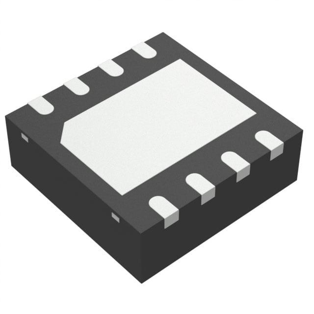
- 型号: FM25L16B-DG
- 制造商: Cypress Semiconductor
- 库位|库存: xxxx|xxxx
- 要求:
| 数量阶梯 | 香港交货 | 国内含税 |
| +xxxx | $xxxx | ¥xxxx |
查看当月历史价格
查看今年历史价格
FM25L16B-DG产品简介:
ICGOO电子元器件商城为您提供FM25L16B-DG由Cypress Semiconductor设计生产,在icgoo商城现货销售,并且可以通过原厂、代理商等渠道进行代购。 FM25L16B-DG价格参考。Cypress SemiconductorFM25L16B-DG封装/规格:存储器, FRAM(铁电体 RAM) 存储器 IC 16Kb (2K x 8) SPI 20MHz 8-TDFN(4x4.5)。您可以下载FM25L16B-DG参考资料、Datasheet数据手册功能说明书,资料中有FM25L16B-DG 详细功能的应用电路图电压和使用方法及教程。
Cypress Semiconductor Corp. 的 FM25L16B-DG 是一款铁电随机存取存储器(FRAM),属于非易失性存储器类别。它具有低功耗、高速读写和高耐久性的特点,适用于多种应用场景。

 1. 工业自动化
FM25L16B-DG 在工业自动化领域中广泛应用。它可以用于数据记录和参数存储,确保在断电情况下数据不丢失。例如,在PLC(可编程逻辑控制器)中,FRAM可以存储运行状态、配置参数和历史数据,提高系统的可靠性和稳定性。

 2. 智能仪表
智能电表、水表和气表等设备需要频繁地记录使用数据。FM25L16B-DG 的高耐久性和快速写入特性使其成为这些应用的理想选择。它可以实时保存用户的使用数据,确保计费准确无误,并且在停电或系统故障时不会丢失数据。

 3. 医疗设备
医疗设备如监护仪、血糖仪和心电图机等对数据的准确性和可靠性要求极高。FM25L16B-DG 可以存储患者的生命体征数据、设备配置参数以及操作日志,确保在突发情况下数据的安全性和完整性。

 4. 物联网(IoT)
在物联网设备中,FM25L16B-DG 可以用于存储传感器数据、设备状态信息和通信日志。其低功耗特性有助于延长电池寿命,而高耐久性则保证了频繁写入操作的可靠性。此外,FRAM的非易失性使得设备在网络中断或电源故障时能够迅速恢复。

 5. 汽车电子
汽车电子系统如发动机控制单元(ECU)、车载信息系统和安全气囊控制系统等需要可靠的存储解决方案。FM25L16B-DG 可以存储关键参数、故障代码和行驶数据,确保车辆的安全性和性能优化。

 6. 消费电子产品
消费电子产品如数码相机、便携式音乐播放器和智能家居设备也需要稳定的存储方案。FM25L16B-DG 可以用于存储用户设置、媒体文件和操作日志,提供更好的用户体验。

总之,FM25L16B-DG 凭借其独特的技术优势,广泛应用于各种需要高可靠性、低功耗和快速响应的场景中,为不同领域的设备提供了稳定的数据存储解决方案。
| 参数 | 数值 |
| 产品目录 | 集成电路 (IC)半导体 |
| 描述 | IC FRAM 16KBIT 20MHZ 8TDFNF-RAM 16K Serial SPI 3V FRAM |
| 产品分类 | |
| 品牌 | Cypress Semiconductor |
| 产品手册 | http://www.cypress.com/?rID=73528 |
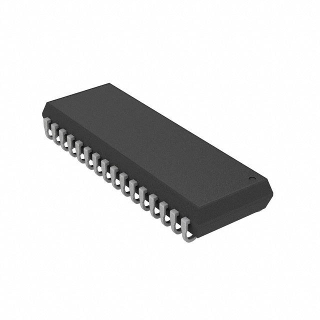
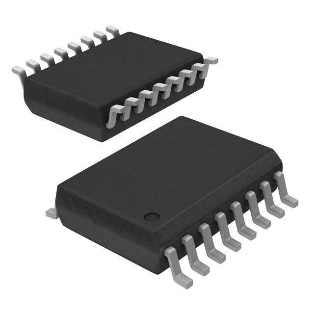
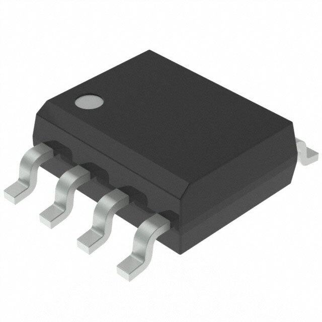
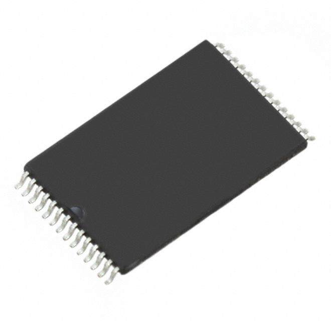
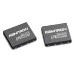
| 产品图片 |
|
| rohs | 符合RoHS无铅 / 符合限制有害物质指令(RoHS)规范要求 |
| 产品系列 | 内存,F-RAM,Cypress Semiconductor FM25L16B-DG- |
| 数据手册 | http://www.cypress.com/?docID=47753 |
| 产品型号 | FM25L16B-DG |
| PCN组件/产地 | http://www.cypress.com/?docID=48502http://www.cypress.com/?docID=48503 |
| PCN设计/规格 | http://www.cypress.com/?docID=45719http://www.cypress.com/?docID=47856 |
| 产品种类 | F-RAM |
| 供应商器件封装 | 8-TDFN(4x4.5) |
| 其它名称 | FM25L16B-DGRA |
| 包装 | 管件 |
| 商标 | Cypress Semiconductor |
| 存储器类型 | FRAM(Ferroelectric RAM) |
| 存储容量 | 16 kbit |
| 安装风格 | SMD/SMT |
| 封装 | Tube |
| 封装/外壳 | 8-VDFN 裸露焊盘 |
| 封装/箱体 | TDFN-8 |
| 工作温度 | -40°C ~ 85°C |
| 工作温度范围 | - 40 C to + 85 C |
| 工作电源电压 | 3.3 V |
| 工厂包装数量 | 81 |
| 接口 | SPI |
| 最大工作温度 | + 85 C |
| 最小工作温度 | - 40 C |
| 标准包装 | 81 |
| 格式-存储器 | RAM |
| 电压-电源 | 2.7 V ~ 3.6 V |
| 电源电压-最大 | 3.6 V |
| 电源电压-最小 | 2.7 V |
| 系列 | FM25L16B-DG |
| 组织 | 2048 x 8 bit |
| 速度 | 20MHz |




- 商务部:美国ITC正式对集成电路等产品启动337调查
- 曝三星4nm工艺存在良率问题 高通将骁龙8 Gen1或转产台积电
- 太阳诱电将投资9.5亿元在常州建新厂生产MLCC 预计2023年完工
- 英特尔发布欧洲新工厂建设计划 深化IDM 2.0 战略
- 台积电先进制程称霸业界 有大客户加持明年业绩稳了
- 达到5530亿美元!SIA预计今年全球半导体销售额将创下新高
- 英特尔拟将自动驾驶子公司Mobileye上市 估值或超500亿美元
- 三星加码芯片和SET,合并消费电子和移动部门,撤换高东真等 CEO
- 三星电子宣布重大人事变动 还合并消费电子和移动部门
- 海关总署:前11个月进口集成电路产品价值2.52万亿元 增长14.8%


PDF Datasheet 数据手册内容提取
FM25L16B 16-Kbit (2K × 8) Serial (SPI) F-RAM 16-Kbit (2K × 8) Serial (SPI) F-RAM Features Functional Description ■16-Kbit ferroelectric random access memory (F-RAM) logically The FM25L16B is a 16-Kbit nonvolatile memory employing an organized as 2K × 8 advanced ferroelectric process. A ferroelectric random access ❐High-endurance 100 trillion (1014) read/writes memory or F-RAM is nonvolatile and performs reads and writes ❐151-year data retention (See Data Retention and Endurance similar to a RAM. It provides reliable data retention for 151 years on page 12) while eliminating the complexities, overhead, and system level ❐NoDelay™ writes reliability problems caused by serial flash, EEPROM, and other ❐Advanced high-reliability ferroelectric process nonvolatile memories. ■Very fast serial peripheral interface (SPI) Unlike serial flash and EEPROM, the FM25L16B performs write ❐Up to 20 MHz frequency operations at bus speed. No write delays are incurred. Data is ❐Direct hardware replacement for serial flash and EEPROM written to the memory array immediately after each byte is ❐Supports SPI mode 0 (0, 0) and mode 3 (1, 1) successfully transferred to the device. The next bus cycle can commence without the need for data polling. In addition, the ■Sophisticated write protection scheme product offers substantial write endurance compared with other ❐Hardware protection using the Write Protect (WP) pin nonvolatile memories. The FM25L16B is capable of supporting ❐Software protection using Write Disable instruction 1014 read/write cycles, or 100 million times more write cycles ❐Software block protection for 1/4, 1/2, or entire array than EEPROM. ■Low power consumption These capabilities make the FM25L16B ideal for nonvolatile ❐200 A active current at 1 MHz memory applications requiring frequent or rapid writes. ❐3 A (typ) standby current Examples range from data collection, where the number of write cycles may be critical, to demanding industrial controls where the ■Low-voltage operation: VDD = 2.7 V to 3.6 V long write time of serial flash or EEPROM can cause data loss. ■Industrial temperature: –40 C to +85 C The FM25L16B provides substantial benefits to users of serial ■Packages EEPROM or flash as a hardware drop-in replacement. The FM25L16B uses the high-speed SPI bus, which enhances the ❐8-pin small outline integrated circuit (SOIC) package high-speed write capability of F-RAM technology. The device ❐8-pin thin dual flat no leads (DFN) package specifications are guaranteed over an industrial temperature ■Restriction of hazardous substances (RoHS) compliant range of –40 C to +85 C. For a complete list of related documentation, click here. Logic Block Diagram WP Instruction Decoder CS Clock Generator HOLD Control Logic Write Protect SCK 2 K x 8 F-RAM Array Instruction Register Address Register 11 8 Counter SI SO Data I /O Register 3 Nonvolatile Status Register CypressSemiconductorCorporation • 198 Champion Court • SanJose, CA 95134-1709 • 408-943-2600 Document Number: 001-84485 Rev. *J Revised November 12, 2018
FM25L16B Contents Pinouts ..............................................................................3 DC Electrical Characteristics ........................................11 Pin Definitions ..................................................................3 Data Retention and Endurance .....................................12 Functional Overview ........................................................4 Capacitance ....................................................................12 Memory Architecture ........................................................4 Thermal Resistance ........................................................12 Serial Peripheral Interface – SPI Bus ..............................4 AC Test Conditions ........................................................12 SPI Overview ...............................................................4 AC Switching Characteristics .......................................13 SPI Modes ...................................................................5 Power Cycle Timing .......................................................15 Power Up to First Access ............................................6 Ordering Information ......................................................16 Command Structure ....................................................6 Ordering Code Definitions .........................................16 WREN - Set Write Enable Latch .................................6 Package Diagrams ..........................................................17 WRDI - Reset Write Enable Latch ...............................6 Acronyms ........................................................................19 Status Register and Write Protection .............................6 Document Conventions .................................................19 RDSR - Read Status Register .....................................7 Units of Measure .......................................................19 WRSR - Write Status Register ....................................7 Document History Page .................................................20 Memory Operation ............................................................8 Sales, Solutions, and Legal Information ......................22 Write Operation ...........................................................8 Worldwide Sales and Design Support .......................22 Read Operation ...........................................................8 Products ....................................................................22 HOLD Pin Operation ...................................................9 PSoC® Solutions ......................................................22 Endurance .................................................................10 Cypress Developer Community .................................22 Maximum Ratings ...........................................................11 Technical Support .....................................................22 Operating Range .............................................................11 Document Number: 001-84485 Rev. *J Page 2 of 22
FM25L16B Pinouts Figure 1. 8-pin SOIC pinout CS 1 8 VDD SO 2 Top View 7 HOLD not to scale WP 3 6 SCK VSS 4 5 SI Figure 2. 8-pin DFN pinout O CS 1 8 VDD SO 2 7 HOLD EXPOSED PAD WP 3 6 SCK VSS 4 5 SI Top View not to scale Pin Definitions Pin Name I/O Type Description CS Input Chip Select. This active LOW input activates the device. When HIGH, the device enters low-power standby mode, ignores other inputs, and tristates the output. When LOW, the device internally activates the SCK signal. A falling edge on CS must occur before every opcode. SCK Input Serial Clock. All I/O activity is synchronized to the serial clock. Inputs are latched on the rising edge and outputs occur on the falling edge. Because the device is synchronous, the clock frequency may be any value between 0 and 20 MHz and may be interrupted at any time. SI[1] Input Serial Input. All data is input to the device on this pin. The pin is sampled on the rising edge of SCK and is ignored at other times. It should always be driven to a valid logic level to meet I specifica- DD tions. SO[1] Output Serial Output. This is the data output pin. It is driven during a read and remains tristated at all other times including when HOLD is LOW. Data transitions are driven on the falling edge of the serial clock. WP Input Write Protect. This active LOW pin prevents write operation to the Status Register when WPEN is set to ‘1’. This is critical because other write protection features are controlled through the Status Register. A complete explanation of write protection is provided in Status Register and Write Protection on page 7. This pin must be tied to V if not used. DD HOLD Input HOLD Pin. The HOLD pin is used when the host CPU must interrupt a memory operation for another task. When HOLD is LOW, the current operation is suspended. The device ignores any transition on SCK or CS. All transitions on HOLD must occur while SCK is LOW. This pin must be tied to V DD if not used. V Power supply Ground for the device. Must be connected to the ground of the system. SS V Power supply Power supply input to the device. DD EXPOSED PAD No connect The EXPOSED PAD on the bottom of 8-pin DFN package is not connected to the die. The EXPOSED PAD should not be soldered on the PCB. Note 1. SI may be connected to SO for a single pin data interface. Document Number: 001-84485 Rev. *J Page 3 of 22
FM25L16B Functional Overview edge of SCK starting from the first rising edge after CS goes active. The FM25L16B is a serial F-RAM memory. The memory array is The SPI protocol is controlled by opcodes. These opcodes logically organized as 2,048 × 8 bits and is accessed using an specify the commands from the bus master to the slave device. industry standard serial peripheral interface (SPI) bus. The After CS is activated, the first byte transferred from the bus functional operation of the F-RAM is similar to serial flash and master is the opcode. Following the opcode, any addresses and serial EEPROMs. The major difference between the FM25L16B data are then transferred. The CS must go inactive after an and a serial flash or EEPROM with the same pinout is the operation is complete and before a new opcode can be issued. F-RAM's superior write performance, high endurance, and low The commonly used terms in the SPI protocol are as follows: power consumption. SPI Master Memory Architecture The SPI master device controls the operations on a SPI bus. An When accessing the FM25L16B, the user addresses 2K SPI bus may have only one master with one or more slave locations of eight data bits each. These eight data bits are shifted devices. All the slaves share the same SPI bus lines and the in or out serially. The addresses are accessed using the SPI master may select any of the slave devices using the CS pin. All protocol, which includes a chip select (to permit multiple devices of the operations must be initiated by the master activating a on the bus), an opcode, and a two-byte address. The upper 5bits slave device by pulling the CS pin of the slave LOW. The master of the address range are 'don't care' values. The complete also generates the SCK and all the data transmission on SI and address of 11 bits specifies each byte address uniquely. SO lines are synchronized with this clock. Most functions of the FM25L16B are either controlled by the SPI SPI Slave interface or handled by on-board circuitry. The access time for the memory operation is essentially zero, beyond the time The SPI slave device is activated by the master through the Chip needed for the serial protocol. That is, the memory is read or Select line. A slave device gets the SCK as an input from the SPI written at the speed of the SPI bus. Unlike a serial flash or master and all the communication is synchronized with this EEPROM, it is not necessary to poll the device for a ready clock. An SPI slave never initiates a communication on the SPI condition because writes occur at bus speed. By the time a new bus and acts only on the instruction from the master. bus transaction can be shifted into the device, a write operation The FM25L16B operates as an SPI slave and may share the SPI is complete. This is explained in more detail in the interface bus with other SPI slave devices. section. Chip Select (CS) Note The FM25L16B contains no power management circuits other than a simple internal power-on reset circuit. It is the user’s To select any slave device, the master needs to pull down the responsibility to ensure that V is within datasheet tolerances corresponding CS pin. Any instruction can be issued to a slave DD to prevent incorrect operation. It is recommended that the part is device only while the CS pin is LOW. When the device is not not powered down with chip enable active. selected, data through the SI pin is ignored and the serial output pin (SO) remains in a high-impedance state. Serial Peripheral Interface – SPI Bus Note A new instruction must begin with the falling edge of CS. The FM25L16B is a SPI slave device and operates at speeds up Therefore, only one opcode can be issued for each active Chip to 20 MHz. This high-speed serial bus provides Select cycle. high-performance serial communication to a SPI master. Many Serial Clock (SCK) common microcontrollers have hardware SPI ports allowing a The Serial Clock is generated by the SPI master and the direct interface. It is quite simple to emulate the port using communication is synchronized with this clock after CS goes ordinary port pins for microcontrollers that do not. The LOW. FM25L16B operates in SPI Mode 0 and 3. The FM25L16B enables SPI modes 0 and 3 for data SPI Overview communication. In both of these modes, the inputs are latched The SPI is a four-pin interface with Chip Select (CS), Serial Input by the slave device on the rising edge of SCK and outputs are (SI), Serial Output (SO), and Serial Clock (SCK) pins. issued on the falling edge. Therefore, the first rising edge of SCK signifies the arrival of the first bit (MSB) of a SPI instruction on The SPI is a synchronous serial interface, which uses clock and the SI pin. Further, all data inputs and outputs are synchronized data pins for memory access and supports multiple devices on with SCK. the data bus. A device on the SPI bus is activated using the CS pin. Data Transmission (SI/SO) The relationship between chip select, clock, and data is dictated The SPI data bus consists of two lines, SI and SO, for serial data by the SPI mode. This device supports SPI modes 0 and 3. In communication. SI is also referred to as Master Out Slave In both of these modes, data is clocked into the F-RAM on the rising (MOSI) and SO is referred to as Master In Slave Out (MISO). The master issues instructions to the slave through the SI pin, while Document Number: 001-84485 Rev. *J Page 4 of 22
FM25L16B the slave responds through the SO pin. Multiple slave devices these three bits are ‘don’t care’, Cypress recommends that these may share the SI and SO lines as described earlier. bits be set to 0s to enable seamless transition to higher memory densities. The FM25L16B has two separate pins for SI and SO, which can be connected with the master as shown in Figure3. Serial Opcode For a microcontroller that has no dedicated SPI bus, a After the slave device is selected with CS going LOW, the first general-purpose port may be used. To reduce hardware byte received is treated as the opcode for the intended operation. resources on the controller, it is possible to connect the two data FM25L16B uses the standard opcodes for memory accesses. pins (SI, SO) together and tie off (HIGH) the HOLD and WP pins. Figure4 shows such a configuration, which uses only three pins. Invalid Opcode If an invalid opcode is received, the opcode is ignored and the Most Significant Bit (MSB) device ignores any additional serial data on the SI pin until the The SPI protocol requires that the first bit to be transmitted is the next falling edge of CS, and the SO pin remains tristated. Most Significant Bit (MSB). This is valid for both address and data transmission. Status Register The 16-Kbit serial F-RAM requires a 2-byte address for any read FM25L16B has an 8-bit Status Register. The bits in the Status or write operation. Because the address is only 11 bits, the first Register are used to configure the device. These bits are five bits which are fed in are ignored by the device. Although described in Table 3 on page 7. Figure 3. System Configuration with SPI port SCK MOSI MISO SCK SI SO SCK SI SO SPI FM25L16B FM25L16B Microcontroller CS HOLD WP CS HOLD WP CS1 HOLD1 WP1 CS2 HOLD2 WP2 Figure 4. System Configuration without SPI port P1.0 P1.1 SCK SI SO Microcontroller FM25L16B CS HOLD WP P1.2 SPI Modes For both these modes, the input data is latched in on the rising edge of SCK starting from the first rising edge after CS goes FM25L16B may be driven by a microcontroller with its SPI active. If the clock starts from a HIGH state (in mode 3), the first peripheral running in either of the following two modes: rising edge after the clock toggles is considered. The output data ■SPI Mode 0 (CPOL = 0, CPHA = 0) is available on the falling edge of SCK. ■SPI Mode 3 (CPOL = 1, CPHA = 1) Document Number: 001-84485 Rev. *J Page 5 of 22
FM25L16B The two SPI modes are shown in Figure5 and Figure6. The WREN - Set Write Enable Latch status of the clock when the bus master is not transferring data is: The FM25L16B will power up with writes disabled. The WREN ■SCK remains at 0 for Mode 0 command must be issued before any write operation. Sending the WREN opcode allows the user to issue subsequent opcodes ■SCK remains at 1 for Mode 3 for write operations. These include writing the Status Register The device detects the SPI mode from the status of the SCK pin (WRSR) and writing the memory (WRITE). when the device is selected by bringing the CS pin LOW. If the Sending the WREN opcode causes the internal Write Enable SCK pin is LOW when the device is selected, SPI Mode 0 is Latch to be set. A flag bit in the Status Register, called WEL, assumed and if the SCK pin is HIGH, it works in SPI Mode3. indicates the state of the latch. WEL = ‘1’ indicates that writes are permitted. Attempting to write the WEL bit in the Status Register Figure 5. SPI Mode 0 has no effect on the state of this bit – only the WREN opcode can set this bit. The WEL bit will be automatically cleared on the rising CS edge of CS following a WRDI, a WRSR, or a WRITE operation. This prevents further writes to the Status Register or the F-RAM 0 1 2 3 4 5 6 7 array without another WREN command. Figure7 illustrates the SCK WREN command bus configuration. Figure 7. WREN Bus Configuration SI 7 6 5 4 3 2 1 0 MSB LSB CS 0 1 2 3 4 5 6 7 SCK Figure 6. SPI Mode 3 SI 0 0 0 0 0 1 1 0 CS 0 1 2 3 4 5 6 7 HI-Z SO SCK WRDI - Reset Write Enable Latch The WRDI command disables all write activity by clearing the SI 7 6 5 4 3 2 1 0 Write Enable Latch. The user can verify that writes are disabled MSB LSB by reading the WEL bit in the Status Register and verifying that WEL is equal to ‘0’. Figure8 illustrates the WRDI command bus Power Up to First Access configuration. The FM25L16B is not accessible for a t time after power up. PU Users must comply with the timing parameter t , which is the PU Figure 8. WRDI Bus Configuration minimum time from V (min) to the first CS LOW. DD CS Command Structure 0 1 2 3 4 5 6 7 There are six commands, called opcodes, that can be issued by the bus master to the FM25L16B. They are listed in Table1. SCK These opcodes control the functions performed by the memory. SI 0 0 0 0 0 1 0 0 Table 1. Opcode commands Name Description Opcode HI-Z SO WREN Set write enable latch 0000 0110b WRDI Write disable 0000 0100b RDSR Read Status Register 0000 0101b WRSR Write Status Register 0000 0001b READ Read memory data 0000 0011b WRITE Write memory data 0000 0010b Document Number: 001-84485 Rev. *J Page 6 of 22
FM25L16B Status Register and Write Protection is organized as follows. (The default value shipped from the factory for bits in the Status Register is ‘0’.) The write protection features of the FM25L16B are multi-tiered and are enabled through the status register. The Status Register Table 2. Status Register Bit 7 Bit 6 Bit 5 Bit 4 Bit 3 Bit 2 Bit 1 Bit 0 WPEN (0) X (0) X (0) X (0) BP1 (0) BP0 (0) WEL (0) X (0) Table 3. Status Register Bit Definition Bit Definition Description Bit 0 Don’t care This bit is non-writable and always returns ‘0’ upon read. Bit 1 (WEL) Write Enable Latch WEL indicates if the device is write enabled. This bit defaults to ‘0’ (disabled) on power-up. WEL = ‘1’ --> Write enabled WEL = ‘0’ --> Write disabled Bit 2 (BP0) Block Protect bit ‘0’ Used for block protection. For details, see Table4. Bit 3 (BP1) Block Protect bit ‘1’ Used for block protection. For details, see Table4. Bit 4-6 Don’t care These bits are non-writable and always return ‘0’ upon read. Bit 7 (WPEN) Write Protect Enable bit Used to enable the function of Write Protect Pin (WP). For details, see Table5. Bits 0 and 4-6 are fixed at ‘0’; none of these bits can be modified. write to the Status Register. Thus the Status Register is Note that bit 0 (“Ready or Write in progress” bit in serial flash and write-protected only when WPEN = ‘1’ and WP = ‘0’. EEPROM) is unnecessary, as the F-RAM writes in real-time and Table5 summarizes the write protection conditions. is never busy, so it reads out as a ‘0’. The BP1 and BP0 control the software write-protection features and are nonvolatile bits. Table 5. Write Protection The WEL flag indicates the state of the Write Enable Latch. Protected Unprotected Status Attempting to directly write the WEL bit in the Status Register has WEL WPEN WP Blocks Blocks Register no effect on its state. This bit is internally set and cleared via the WREN and WRDI commands, respectively. 0 X X Protected Protected Protected 1 0 X Protected Unprotected Unprotected BP1 and BP0 are memory block write protection bits. They specify portions of memory that are write-protected as shown in 1 1 0 Protected Unprotected Protected Table4. 1 1 1 Protected Unprotected Unprotected Table 4. Block Memory Write Protection RDSR - Read Status Register BP1 BP0 Protected Address Range The RDSR command allows the bus master to verify the 0 0 None contents of the Status Register. Reading the status register 0 1 600h to 7FFh (upper 1/4) provides information about the current state of the 1 0 400h to 7FFh (upper 1/2) write-protection features. Following the RDSR opcode, the FM25L16B will return one byte with the contents of the Status 1 1 000h to 7FFh (all) Register. The BP1 and BP0 bits and the Write Enable Latch are the only WRSR - Write Status Register mechanisms that protect the memory from writes. The remaining The WRSR command allows the SPI bus master to write into the write protection features protect inadvertent changes to the block Status Register and change the write protect configuration by protect bits. setting the WPEN, BP0 and BP1 bits as required. Before issuing The write protect enable bit (WPEN) in the Status Register a WRSR command, the WP pin must be HIGH or inactive. Note controls the effect of the hardware write protect (WP) pin. When that on the FM25L16B, WP only prevents writing to the Status the WPEN bit is set to ‘0’, the status of the WP pin is ignored. Register, not the memory array. Before sending the WRSR When the WPEN bit is set to ‘1’, a LOW on the WP pin inhibits a command, the user must send a WREN command to enable writes. Executing a WRSR command is a write operation and therefore, clears the Write Enable Latch. Document Number: 001-84485 Rev. *J Page 7 of 22
FM25L16B Figure 9. RDSR Bus Configuration CS 0 1 2 3 4 5 6 7 0 1 2 3 4 5 6 7 SCK Opcode SI 0 0 0 0 0 1 0 1 0 Data HI-Z SO D7 D6 D5 D4 D3 D2 D1 D0 MSB LSB Figure 10. WRSR Bus Configuration (WREN not shown) CS 0 1 2 3 4 5 6 7 0 1 2 3 4 5 6 7 SCK Opcode Data SI 0 0 0 0 0 0 0 1 D7 X X X D3 D2 X X MSB LSB HI-Z SO Memory Operation operations. F-RAM memories do not have page buffers because each byte is written to the F-RAM array immediately after it is The SPI interface, which is capable of a high clock frequency, clocked in (after the eighth clock). This allows any number of highlights the fast write capability of the F-RAM technology. bytes to be written without page buffer delays. Unlike serial flash and EEPROMs, the FM25L16B can perform Note If the power is lost in the middle of the write operation, only sequential writes at bus speed. No page register is needed and the last completed byte will be written. any number of sequential writes may be performed. Read Operation Write Operation After the falling edge of CS, the bus master can issue a READ All writes to the memory begin with a WREN opcode. The WRITE opcode. Following the READ command is a two-byte address opcode is followed by a two-byte address containing the 11-bit containing the 11-bit address (A10–A0) of the first byte of the address (A10–A0) of the first data byte to be written into the read operation. The upper five bits of the address are ignored. memory. The upper five bits of the two-byte address are ignored. After the opcode and address are issued, the device drives out Subsequent bytes are data bytes, which are written sequentially. the read data on the next eight clocks. The SI input is ignored Addresses are incremented internally as long as the bus master during read data bytes. Subsequent bytes are data bytes, which continues to issue clocks and keeps CS LOW. If the last address are read out sequentially. Addresses are incremented internally of 7FFh is reached, the counter will roll over to 000h. Data is as long as the bus master continues to issue clocks and CS is written MSB first. The rising edge of CS terminates a write LOW. If the last address of 7FFh is reached, the counter will roll operation. A write operation is shown in Figure 11 on page 9. over to 000h. Data is read MSB first. The rising edge of CS Note When a burst write reaches a protected block address, the terminates a read operation and tristates the SO pin. A read automatic address increment stops and all the subsequent data operation is shown in Figure 12 on page 9. bytes received for write will be ignored by the device. EEPROMs use page buffers to increase their write throughput. This compensates for the technology’s inherently slow write Document Number: 001-84485 Rev. *J Page 8 of 22
FM25L16B Figure 11. Memory Write (WREN not shown) CS 0 1 2 3 4 5 6 7 0 1 2 3 4 5 6 7 12 13 14 15 0 1 2 3 4 5 6 7 ~~ SCK Opcode 11-bit Address Data ~~ SI 0 0 0 0 0 0 1 0 X X X X X A10A9 A8 A3 A2 A1 A0 D7 D6 D5 D4 D3 D2 D1 D0 MSB LSBMSB LSB HI-Z SO Figure 12. Memory Read CS 0 1 2 3 4 5 6 7 0 1 2 3 4 5 6 7 12 13 14 15 0 1 2 3 4 5 6 7 ~~ SCK Opcode 11-bit Address ~~ SI 0 0 0 0 0 0 1 1 X X X X X A10 A9 A8 A3 A2 A1 A0 MSB LSB Data HI-Z SO D7 D6 D5 D4 D3 D2 D1 D0 MSB LSB HOLD Pin Operation HIGH while SCK is LOW will resume an operation. The transitions of HOLD must occur while SCK is LOW, but the SCK The HOLD pin can be used to interrupt a serial operation without and CS pin can toggle during a hold state. aborting it. If the bus master pulls the HOLD pin LOW while SCK is LOW, the current operation will pause. Taking the HOLD pin Figure 13. HOLD Operation[2] ~~ CS ~~ SCK HOLD ~~ ~~ SI VALID IN VALID IN ~~ SO Note 2. Figure shows HOLD operation for input mode and output mode. Document Number: 001-84485 Rev. *J Page 9 of 22
FM25L16B Endurance F-RAM read and write endurance is virtually unlimited even at a 20 MHz clock rate. The FM25L16B devices are capable of being accessed at least 1014 times, reads or writes. An F-RAM memory operates with a Table 6. Time to Reach Endurance Limit for Repeating read and restore mechanism. Therefore, an endurance cycle is 64-byte Loop applied on a row basis for each access (read or write) to the memory array. The F-RAM architecture is based on an array of SCK Freq Endurance Endurance Years to Reach rows and columns of 256 rows of 64-bits each. The entire row is (MHz) Cycles/sec Cycles/year Limit internally accessed once whether a single byte or all eight bytes 20 37,310 1.18 × 10¹² 85.1 are read or written. Each byte in the row is counted only once in 10 18,660 5.88 × 10¹¹ 170.2 an endurance calculation. Table6 shows endurance calculations for a 64-byte repeating loop, which includes an opcode, a starting 5 9,330 2.94 × 10¹¹ 340.3 address, and a sequential 64-byte data stream. This causes each byte to experience one endurance cycle through the loop. Document Number: 001-84485 Rev. *J Page 10 of 22
FM25L16B Maximum Ratings Package power dissipation capability (T = 25 °C) .................................................................1.0 W A Exceeding maximum ratings may shorten the useful life of the Surface mount lead soldering temperature device. These user guidelines are not tested. (3 seconds) ..............................................................+260 C Storage temperature ................................–65 C to +125 C DC output current Maximum accumulated storage time (1 output at a time, 1s duration) ..................................15 mA At 125 °C ambient temperature .................................1000 h Electrostatic Discharge Voltage [3] At 85 °C ambient temperature ................................10 Years Human Body Model (AEC-Q100-002 Rev. E) ................... 2 kV Ambient temperature Charged Device Model (AEC-Q100-011 Rev. B) ..............500 V with power applied ...................................–55 °C to +125 °C Latch-up current ....................................................> 140 mA Supply voltage on V relative to V .........–1.0 V to +5.0 V DD SS Operating Range Input voltage .............–1.0 V to +5.0 V and V < V +1.0 V IN DD DC voltage applied to outputs Range Ambient Temperature (T ) V A DD in High Z state ....................................–0.5 V to VDD + 0.5 V Industrial –40 C to +85 C 2.7 V to 3.6 V Transient voltage (< 20 ns) on any pin to ground potential ............–2.0 V to V + 2.0 V DD DC Electrical Characteristics Over the Operating Range Parameter Description Test Conditions Min Typ [4] Max Unit V Power supply 2.7 3.3 3.6 V DD I V supply current SCK toggling between f = 1 MHz – – 0.2 mA DD DD SCK V – 0.3 V and V , DD SS f = 20 MHz – – 3 mA other inputs V or SCK SS V – 0.3 V. DD SO = Open. I V standby current CS = V . All other inputs V or V . – 3 6 A SB DD DD SS DD I Input leakage current V < V < V – – ±1 A LI SS IN DD I Output leakage current V < V < V – – ±1 A LO SS OUT DD V Input HIGH voltage 0.7 × V – V + 0.3 V IH DD DD V Input LOW voltage – 0.3 – 0.3 × V V IL DD V Output HIGH voltage I = –2 mA V – 0.8 – – V OH OH DD V Output LOW voltage I = 2 mA – – 0.4 V OL OL V [5] Input Hysteresis (CS and SCK 0.05 × V – – V HYS DD pin) Notes 3. Electrostatic Discharge voltages specified in the datasheet are the JEDEC standard limits used for qualifying the device. To know the maximum value device passes for, please refer to the device qualification report available on the website. 4. Typical values are at 25 °C, VDD = VDD(typ). Not 100% tested. 5. This parameter is characterized and not 100% tested. Document Number: 001-84485 Rev. *J Page 11 of 22
FM25L16B Data Retention and Endurance Parameter Description Test condition Min Max Unit T Data retention T = 85 C 10 – Years DR A T = 75 C 38 – A T = 65 C 151 – A NV Endurance Over operating temperature 1014 – Cycles C Capacitance Parameter [6] Description Test Conditions Max Unit C Output pin capacitance (SO) T = 25 C, f = 1 MHz, V = V (typ) 8 pF O A DD DD C Input pin capacitance 6 pF I Thermal Resistance Parameter [6] Description Test Conditions 8-pin SOIC 8-pin DFN Unit Thermal resistance Test conditions follow standard test 147 19 C/W JA (junction to ambient) methods and procedures for measuring Thermal resistance thermal impedance, per EIA/JESD51. 47 30 C/W JC (junction to case) AC Test Conditions Input pulse levels .................................10% and 90% of V DD Input rise and fall times ...................................................5 ns Input and output timing reference levels ................0.5 × V DD Output load capacitance ..............................................30 pF Note 6. This parameter is characterized and not 100% tested. Document Number: 001-84485 Rev. *J Page 12 of 22
FM25L16B AC Switching Characteristics Over the Operating Range Parameters [7] Cypress Description Min Max Unit Alt. Parameter Parameter f – SCK Clock frequency 0 20 MHz SCK t – Clock HIGH time 22 – ns CH t – Clock LOW time 22 – ns CL t t Chip select setup 10 – ns CSU CSS t t Chip select hold 10 – ns CSH CSH t [8, 9] t Output disable time – 20 ns OD HZCS t t Output data valid time – 20 ns ODV CO t – Output hold time 0 – ns OH t – Deselect time 60 – ns D t [10, 11] – Data in rise time – 50 ns R t [10, 11] – Data in fall time – 50 ns F t t Data setup time 5 – ns SU SD t t Data hold time 5 – ns H HD t t HOLD setup time 10 – ns HS SH t t HOLD hold time 10 – ns HH HH t [8, 9] t HOLD LOW to HI-Z – 20 ns HZ HHZ t [9] t HOLD HIGH to data active – 20 ns LZ HLZ Notes 7. Test conditions assume a signal transition time of 5 ns or less, timing reference levels of 0.5 × VDD, input pulse levels of 10% to 90% of VDD, and output loading of the specified IOL/IOH and 30 pF load capacitance shown in AC Test Conditions on page 12. 8. tOD and tHZ are specified with a load capacitance of 5 pF. Transition is measured when the outputs enter a high impedance state. 9. This parameter is characterized and not 100% tested. 10.Rise and fall times measured between 10% and 90% of waveform. 11.These parameters are guaranteed by design and are not tested. Document Number: 001-84485 Rev. *J Page 13 of 22
FM25L16B Figure 14. Synchronous Data Timing (Mode 0) tD CS tCSU tCH tCL tCSH SCK tSU tH SI VALID IN VALID IN VALID IN tODV tOH tOD HI-Z HI-Z SO Figure 15. HOLD Timing ~~ CS ~~ SCK tHH tHH tHS tHS HOLD ~~ tSU ~~ SI VALID IN VALID IN tHZ tLZ ~~ SO Document Number: 001-84485 Rev. *J Page 14 of 22
FM25L16B Power Cycle Timing Over the Operating Range Parameter Description Min Max Unit tPU Power-up VDD(min) to first access (CS LOW) 1 – ms tPD Last access (CS HIGH) to power-down (VDD(min)) 0 – µs tVR [12] VDD power-up ramp rate 30 – µs/V tVF [12] VDD power-down ramp rate 30 – µs/V Figure 16. Power Cycle Timing ~~ VDD(min) VDD(min) VDD tVR tVF tPU tPD CS ~~ Note 12.Slope measured at any point on VDD waveform. Document Number: 001-84485 Rev. *J Page 15 of 22
FM25L16B Ordering Information Package Operating Ordering Code Package Type Diagram Range FM25L16B-G 51-85066 8-pin SOIC Industrial FM25L16B-GTR 51-85066 8-pin SOIC FM25L16B-DG 001-85260 8-pin DFN FM25L16B-DGTR 001-85260 8-pin DFN All these parts are Pb-free. Contact your local Cypress sales representative for availability of these parts. Ordering Code Definitions FM 25 L 16 B - X X Option: X = blank or TR blank = Standard; TR = Tape and Reel Package Type: X = G or DG G = 8-pin SOIC; DG = 8-pin DFN Die revision Density: 16 = 16-Kbit Voltage: L = 2.7 V to 3.6 V SPI F-RAM Cypress Document Number: 001-84485 Rev. *J Page 16 of 22
FM25L16B Package Diagrams Figure 17. 8-pin SOIC (150 Mils) Package Outline, 51-85066 51-85066 *I Document Number: 001-84485 Rev. *J Page 17 of 22
FM25L16B Package Diagrams (continued) Figure 18. 8-pin DFN (4.0 mm × 4.5 mm × 0.8 mm) Package Outline, 001-85260 001-85260 *B Document Number: 001-84485 Rev. *J Page 18 of 22
FM25L16B Acronyms Document Conventions Units of Measure Acronym Description AEC Automotive Electronics Council Symbol Unit of Measure CPHA Clock Phase °C degree Celsius Hz hertz CPOL Clock Polarity kHz kilohertz DFN Dual Flat No-lead K kilohm EEPROM Electrically Erasable Programmable Read-Only Memory Kbit kilobit kV kilovolt EIA Electronic Industries Alliance MHz megahertz I/O Input/Output A microampere JEDEC Joint Electron Devices Engineering Council s microsecond JESD JEDEC Standards mA milliampere LSB Least Significant Bit ms millisecond MSB Most Significant Bit ns nanosecond F-RAM Ferroelectric Random Access Memory ohm RoHS Restriction of Hazardous Substances % percent SPI Serial Peripheral Interface pF picofarad SOIC Small Outline Integrated Circuit V volt W watt Document Number: 001-84485 Rev. *J Page 19 of 22
FM25L16B Document History Page Document Title: FM25L16B, 16-Kbit (2K × 8) Serial (SPI) F-RAM Document Number: 001-84485 Orig. of Submission Rev. ECN No. Description of Change Change Date ** 3902952 GVCH 02/25/2013 New spec. *A 3924523 GVCH 03/07/2013 Updated Power Cycle Timing: Changed minimum value of t parameter from 10 ms to 1 ms. PU *B 3994285 GVCH 05/14/2013 Added Appendix A - Errata for FM25L16B. *C 4045438 GVCH 06/30/2013 All errata items are fixed and the errata is removed. *D 4217167 GVCH 01/28/2014 Updated Pinouts: Updated Figure2 (Added EXPOSED PAD details). Updated Pin Definitions: Added EXPOSED PAD pin and its corresponding details. Updated Maximum Ratings: Added “Maximum Junction Temperature” and its corresponding details. Added “DC voltage applied to outputs in High-Z state” and its corresponding details. Added “Transient voltage (< 20 ns) on any pin to ground potential” and its corresponding details. Added “Package power dissipation capability (T = 25 °C)” and its A corresponding details. Added “DC output current (1 output at a time, 1s duration)” and its corresponding details. Added “Latch-up Current” and its corresponding details. Removed “Package Moisture Sensitivity Level” and its corresponding details. Updated Data Retention and Endurance: Removed details of T parameter corresponding to “T = +80 °C”. DR A Added details of T parameter corresponding to “T = 65 °C”. DR A Added NV parameter and its details. C Added Thermal Resistance. Updated Package Diagrams: Removed Package Marking Scheme (top mark). Removed “Ramtron Revision History”. Updated to Cypress template. Completing Sunset Review. *E 4569028 GVCH 11/13/2014 Updated Functional Description: Added “For a complete list of related documentation, click here.” at the end. *F 4786822 GVCH 06/04/2015 Replaced “TDFN” with “DFN” in all instances across the document. Updated Pin Definitions: Updated details in “Description” column of “EXPOSED PAD” pin. Updated Package Diagrams: spec 51-85066 – Changed revision from *F to *G. spec 001-85260 – Changed revision from *A to *B. Updated to new template. *G 4878568 ZSK / PSR 08/10/2015 Updated Maximum Ratings: Removed “Maximum junction temperature” and its corresponding details. Added “Maximum accumulated storage time” and its corresponding details. Added “Ambient temperature with power applied” and its corresponding details. Document Number: 001-84485 Rev. *J Page 20 of 22
FM25L16B Document History Page (continued) Document Title: FM25L16B, 16-Kbit (2K × 8) Serial (SPI) F-RAM Document Number: 001-84485 Orig. of Submission Rev. ECN No. Description of Change Change Date *H 5606837 GVCH 01/27/2017 Updated Maximum Ratings: Updated Electrostatic Discharge Voltage (in compliance with AEC-Q100 standard): Changed value of “Human Body Model” from 4 kV to 2 kV. Changed value of “Charged Device Model” from 1.25 kV to 500 V. Removed “Machine Model” related information. Updated Package Diagrams: spec 51-85066 – Changed revision from *G to *H. Updated to new template. Completing Sunset Review. *I 5713284 GVCH 04/26/2017 Updated Maximum Ratings: Added Note 3 and referred the same note in “Electrostatic Discharge Voltage”. Updated to new template. *J 6237906 GVCH 11/12/2018 Updated Maximum Ratings: Replaced “–55 °C to +125 °C” with “–65 °C to +125 °C” in ratings corresponding to “Storage temperature”. Updated Package Diagrams: spec 51-85066 – Changed revision from *H to *I. Updated to new template. Document Number: 001-84485 Rev. *J Page 21 of 22
FM25L16B Sales, Solutions, and Legal Information Worldwide Sales and Design Support Cypress maintains a worldwide network of offices, solution centers, manufacturer’s representatives, and distributors. To find the office closest to you, visit us at Cypress Locations. Products PSoC® Solutions Arm® Cortex® Microcontrollers cypress.com/arm PSoC 1 | PSoC 3 | PSoC 4 | PSoC 5LP | PSoC 6 MCU Automotive cypress.com/automotive Cypress Developer Community Clocks & Buffers cypress.com/clocks Community | Projects | Video | Blogs | Training | Components Interface cypress.com/interface Technical Support Internet of Things cypress.com/iot cypress.com/support Memory cypress.com/memory Microcontrollers cypress.com/mcu PSoC cypress.com/psoc Power Management ICs cypress.com/pmic Touch Sensing cypress.com/touch USB Controllers cypress.com/usb Wireless Connectivity cypress.com/wireless © Cypress Semiconductor Corporation, 2013–2018. This document is the property of Cypress Semiconductor Corporation and its subsidiaries, including Spansion LLC (“Cypress”). This document, including any software or firmware included or referenced in this document (“Software”), is owned by Cypress under the intellectual property laws and treaties of the United States and other countries worldwide. Cypress reserves all rights under such laws and treaties and does not, except as specifically stated in this paragraph, grant any license under its patents, copyrights, trademarks, or other intellectual property rights. If the Software is not accompanied by a license agreement and you do not otherwise have a written agreement with Cypress governing the use of the Software, then Cypress hereby grants you a personal, non-exclusive, nontransferable license (without the right to sublicense) (1) under its copyright rights in the Software (a) for Software provided in source code form, to modify and reproduce the Software solely for use with Cypress hardware products, only internally within your organization, and (b) to distribute the Software in binary code form externally to end users (either directly or indirectly through resellers and distributors), solely for use on Cypress hardware product units, and (2) under those claims of Cypress’s patents that are infringed by the Software (as provided by Cypress, unmodified) to make, use, distribute, and import the Software solely for use with Cypress hardware products. Any other use, reproduction, modification, translation, or compilation of the Software is prohibited. TO THE EXTENT PERMITTED BY APPLICABLE LAW, CYPRESS MAKES NO WARRANTY OF ANY KIND, EXPRESS OR IMPLIED, WITH REGARD TO THIS DOCUMENT OR ANY SOFTWARE OR ACCOMPANYING HARDWARE, INCLUDING, BUT NOT LIMITED TO, THE IMPLIED WARRANTIES OF MERCHANTABILITY AND FITNESS FOR A PARTICULAR PURPOSE. No computing device can be absolutely secure. Therefore, despite security measures implemented in Cypress hardware or software products, Cypress does not assume any liability arising out of any security breach, such as unauthorized access to or use of a Cypress product. In addition, the products described in these materials may contain design defects or errors known as errata which may cause the product to deviate from published specifications. To the extent permitted by applicable law, Cypress reserves the right to make changes to this document without further notice. Cypress does not assume any liability arising out of the application or use of any product or circuit described in this document. Any information provided in this document, including any sample design information or programming code, is provided only for reference purposes. It is the responsibility of the user of this document to properly design, program, and test the functionality and safety of any application made of this information and any resulting product. Cypress products are not designed, intended, or authorized for use as critical components in systems designed or intended for the operation of weapons, weapons systems, nuclear installations, life-support devices or systems, other medical devices or systems (including resuscitation equipment and surgical implants), pollution control or hazardous substances management, or other uses where the failure of the device or system could cause personal injury, death, or property damage (“Unintended Uses”). A critical component is any component of a device or system whose failure to perform can be reasonably expected to cause the failure of the device or system, or to affect its safety or effectiveness. Cypress is not liable, in whole or in part, and you shall and hereby do release Cypress from any claim, damage, or other liability arising from or related to all Unintended Uses of Cypress products. You shall indemnify and hold Cypress harmless from and against all claims, costs, damages, and other liabilities, including claims for personal injury or death, arising from or related to any Unintended Uses of Cypress products. Cypress, the Cypress logo, Spansion, the Spansion logo, and combinations thereof, WICED, PSoC, CapSense, EZ-USB, F-RAM, and Traveo are trademarks or registered trademarks of Cypress in the United States and other countries. For a more complete list of Cypress trademarks, visit cypress.com. Other names and brands may be claimed as property of their respective owners. Document Number: 001-84485 Rev. *J Revised November 12, 2018 Page 22 of 22
 Datasheet下载