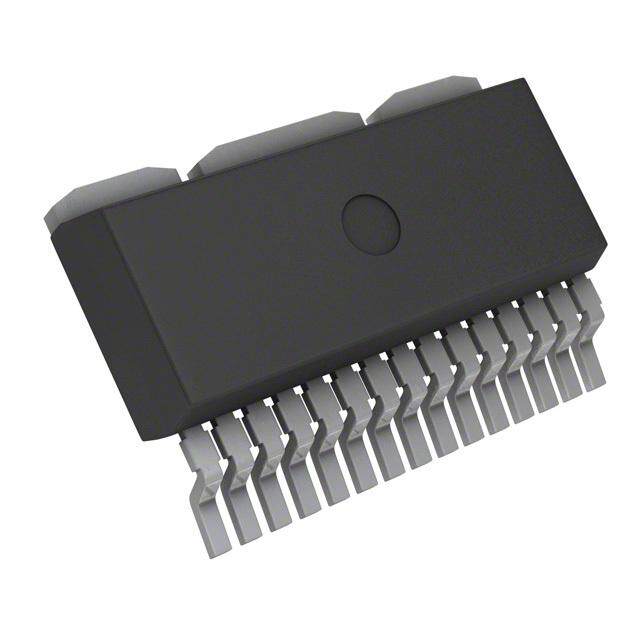
ICGOO在线商城 > 集成电路(IC) > PMIC - 全,半桥驱动器 > FDMF6824B
 Datasheet下载
- 型号: FDMF6824B
- 制造商: Fairchild Semiconductor
- 库位|库存: xxxx|xxxx
- 要求:
| 数量阶梯 | 香港交货 | 国内含税 |
| +xxxx | $xxxx | ¥xxxx |
查看当月历史价格
查看今年历史价格
FDMF6824B产品简介:
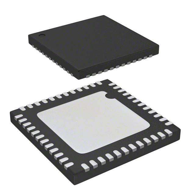
ICGOO电子元器件商城为您提供FDMF6824B由Fairchild Semiconductor设计生产,在icgoo商城现货销售,并且可以通过原厂、代理商等渠道进行代购。 FDMF6824B价格参考。Fairchild SemiconductorFDMF6824B封装/规格:PMIC - 全,半桥驱动器, Half Bridge Driver Synchronous Buck Converters DrMOS 40-PQFN (6x6)。您可以下载FDMF6824B参考资料、Datasheet数据手册功能说明书,资料中有FDMF6824B 详细功能的应用电路图电压和使用方法及教程。
FDMF6824B 是一款由 ON Semiconductor(安森美半导体)生产的功率管理集成电路 (PMIC),属于全桥和半桥驱动器类别。该器件广泛应用于需要高效功率转换和电机驱动的场景,以下是其主要应用场景:

1. 电机控制:
   FDMF6824B 适用于各种类型的电机驱动应用,例如直流无刷电机 (BLDC)、步进电机和其他小型电机。它能够提供高效的驱动能力,支持正向和反向旋转,以及调速功能,适合家用电器(如风扇、泵)和工业设备中的电机控制。

2. 电源管理:
   作为 PMIC 的一部分,FDMF6824B 可用于设计开关模式电源 (SMPS) 和 DC-DC 转换器。它支持高效率的能量转换,适用于适配器、充电器以及其他便携式电子设备的电源管理系统。

3. 汽车电子:
   在汽车领域,FDMF6824B 可用于电动车窗、雨刷器、座椅调节系统和冷却风扇等应用。其高性能和可靠性使其成为汽车电子的理想选择,尤其是在需要紧凑设计和低功耗的场合。

4. 消费类电子产品:
   该器件还可用于消费类电子产品,如打印机、扫描仪和投影仪中的步进电机或小型直流电机驱动。其集成的保护功能(如过流保护和热关断)确保了系统的稳定性和安全性。

5. 工业自动化:
   在工业自动化领域,FDMF6824B 能够驱动伺服电机和其他精密控制设备,满足工厂自动化、机器人技术和运动控制系统的需求。

总之,FDMF6824B 凭借其高效能、高可靠性和多功能性,适用于多种需要功率转换和电机驱动的应用场景,特别是在对成本敏感且空间受限的设计中表现尤为突出。
| 参数 | 数值 |
| 产品目录 | 集成电路 (IC)半导体 |
| 描述 | MODULE DRMOS 55A 40-PQFN门驱动器 DrMOS 55A 5V |
| 产品分类 | PMIC - MOSFET,电桥驱动器 - 内部开关集成电路 - IC |
| 品牌 | Fairchild Semiconductor |
| 产品手册 | |
| 产品图片 | |
| rohs | 符合RoHS无铅 / 符合限制有害物质指令(RoHS)规范要求 |
| 产品系列 | 电源管理 IC,门驱动器,Fairchild Semiconductor FDMF6824BXS™ DrMOS |
| 数据手册 | |
| 产品型号 | FDMF6824B |
| PCN组件/产地 | |
| 上升时间 | 10 ns |
| 下降时间 | 10 ns |
| 产品 | MOSFET Gate Drivers |
| 产品种类 | 门驱动器 |
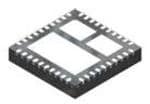
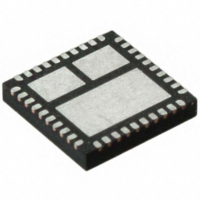
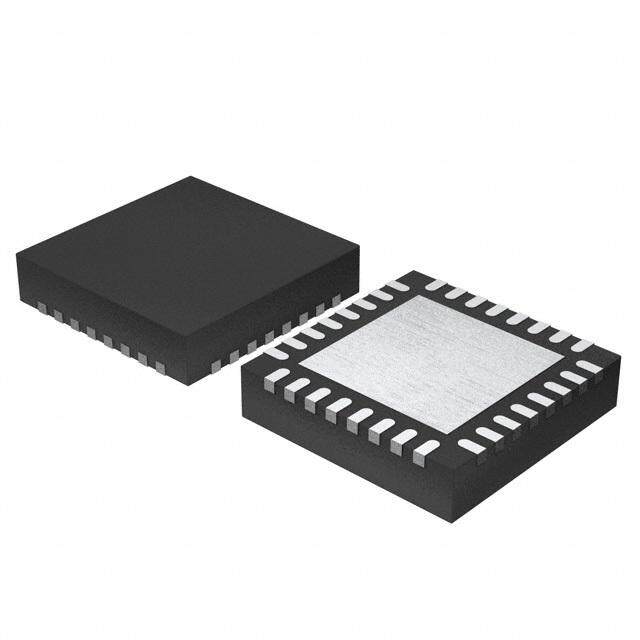
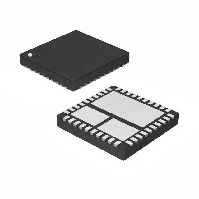
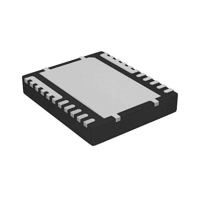
| 供应商器件封装 | 40-PQFN(6x6) |
| 其它名称 | FDMF6824BCT |
| 包装 | 剪切带 (CT) |
| 单位重量 | 224 mg |
| 商标 | Fairchild Semiconductor |
| 安装类型 | 表面贴装 |
| 安装风格 | SMD/SMT |
| 导通电阻 | - |
| 封装 | Reel |
| 封装/外壳 | 40-PowerTFQFN |
| 封装/箱体 | PQFN-40 |
| 工作温度 | -40°C ~ 125°C |
| 工厂包装数量 | 3000 |
| 最大工作温度 | + 125 C |
| 最小工作温度 | - 40 C |
| 标准包装 | 1 |
| 激励器数量 | 2 Driver |
| 电压-电源 | 4.5 V ~ 5.5 V |
| 电流-峰值输出 | - |
| 电流-输出/通道 | 55A |
| 电源电压-最大 | 5.5 V |
| 电源电压-最小 | 4.5 V |
| 电源电流 | 2 mA |
| 类型 | 高端/低端驱动器 |
| 系列 | FDMF6824 |
| 输入类型 | PWM |
| 输出数 | 1 |
| 输出电流 | 55 A |
| 输出端数量 | 1 |
| 配置 | Non-Inverting |


- 商务部:美国ITC正式对集成电路等产品启动337调查
- 曝三星4nm工艺存在良率问题 高通将骁龙8 Gen1或转产台积电
- 太阳诱电将投资9.5亿元在常州建新厂生产MLCC 预计2023年完工
- 英特尔发布欧洲新工厂建设计划 深化IDM 2.0 战略
- 台积电先进制程称霸业界 有大客户加持明年业绩稳了
- 达到5530亿美元!SIA预计今年全球半导体销售额将创下新高
- 英特尔拟将自动驾驶子公司Mobileye上市 估值或超500亿美元
- 三星加码芯片和SET,合并消费电子和移动部门,撤换高东真等 CEO
- 三星电子宣布重大人事变动 还合并消费电子和移动部门
- 海关总署:前11个月进口集成电路产品价值2.52万亿元 增长14.8%

PDF Datasheet 数据手册内容提取
Is Now Part of To learn more about ON Semiconductor, please visit our website at www.onsemi.com Please note: As part of the Fairchild Semiconductor integration, some of the Fairchild orderable part numbers will need to change in order to meet ON Semiconductor’s system requirements. Since the ON Semiconductor product management systems do not have the ability to manage part nomenclature that utilizes an underscore (_), the underscore (_) in the Fairchild part numbers will be changed to a dash (-). This document may contain device numbers with an underscore (_). Please check the ON Semiconductor website to verify the updated device numbers. The most current and up-to-date ordering information can be found at www.onsemi.com. Please email any questions regarding the system integration to Fairchild_questions@onsemi.com. ON Semiconductor and the ON Semiconductor logo are trademarks of Semiconductor Components Industries, LLC dba ON Semiconductor or its subsidiaries in the United States and/or other countries. ON Semiconductor owns the rights to a number of patents, trademarks, copyrights, trade secrets, and other intellectual property. A listing of ON Semiconductor’s product/patent coverage may be accessed at www.onsemi.com/site/pdf/Patent-Marking.pdf. ON Semiconductor reserves the right to make changes without further notice to any products herein. ON Semiconductor makes no warranty, representation or guarantee regarding the suitability of its products for any particular purpose, nor does ON Semiconductor assume any liability arising out of the application or use of any product or circuit, and specifically disclaims any and all liability, including without limitation special, consequential or incidental damages. Buyer is responsible for its products and applications using ON Semiconductor products, including compliance with all laws, regulations and safety requirements or standards, regardless of any support or applications information provided by ON Semiconductor. “Typical” parameters which may be provided in ON Semiconductor data sheets and/or specifications can and do vary in different applications and actual performance may vary over time. All operating parameters, including “Typicals” must be validated for each customer application by customer’s technical experts. ON Semiconductor does not convey any license under its patent rights nor the rights of others. ON Semiconductor products are not designed, intended, or authorized for use as a critical component in life support systems or any FDA Class 3 medical devices or medical devices with a same or similar classification in a foreign jurisdiction or any devices intended for implantation in the human body. Should Buyer purchase or use ON Semiconductor products for any such unintended or unauthorized application, Buyer shall indemnify and hold ON Semiconductor and its officers, employees, subsidiaries, affiliates, and distributors harmless against all claims, costs, damages, and expenses, and reasonable attorney fees arising out of, directly or indirectly, any claim of personal injury or death associated with such unintended or unauthorized use, even if such claim alleges that ON Semiconductor was negligent regarding the design or manufacture of the part. ON Semiconductor is an Equal Opportunity/Affirmative Action Employer. This literature is subject to all applicable copyright laws and is not for resale in any manner.
F D M F 6 January 2014 8 2 4 B — E x FDMF6824B — Extra-Small, High-Performance, t r a - High-Frequency DrMOS Module S m a l l, H Benefits Description ig h Ultra-Compact 6x6 mm PQFN, 72% Space-Saving The XS™ DrMOS family is Fairchild’s next-generation, -P Compared to Conventional Discrete Solutions fully optimized, ultra-compact, integrated MOSFET plus e r Fully Optimized System Efficiency driver power stage solution for high-current, high- fo frequency, synchronous buck DC-DC applications. The r m Clean Switching Waveforms with Minimal Ringing FDMF6824B integrates a driver IC, two power a High-Current Handling MthOerSmFaEllTy se,n haanndc ead , ublotroat-sctorampp aScct h6oxt6tkmym d pioadceka ginet.o a nc e Features With an integrated approach, the complete switching , H Over 93% Peak-Efficiency power stage is optimized with regard to driver and ig MOSFET dynamic performance, system inductance, h High-Current Handling: 55 A and power MOSFET RDS(ON). XS™ DrMOS uses -F High-Performance PQFN Copper-Clip Package Fteacihrcnhoilldo'gsy , hwighhi-cphe rdforarmmaanticcea llyP orewdeurcTeres nscwh®it chM OrinSgFinEgT, req u 3-State 5 V PWM Input Driver eliminating the need for snubber circuit in most buck e converter applications. n Skip-Mode SMOD# (Low-Side Gate Turn Off) Input c y A driver IC with reduced dead times and propagation Thermal Warning Flag for Over-Temperature D delays further enhances the performance. A thermal Condition r warning function warns of a potential over-temperature M Driver Output Disable Function (DISB# Pin) situation. The FDMF6824B also incorporates a Skip O Mode (SMOD#) for improved light-load efficiency. The S Internal Pull-Up and Pull-Down for SMOD# and FDMF6824B also provides a 3-state 5 V PWM input for M DISB# Inputs, Respectively compatibility with a wide range of PWM controllers. o d Fairchild PowerTrench® Technology MOSFETs for u Applications Clean Voltage Waveforms and Reduced Ringing le Fairchild SyncFET™ (Integrated Schottky Diode) High-Performance Gaming Motherboards Technology in Low-Side MOSFET Compact Blade Servers, V-Core and Non-V-Core Integrated Bootstrap Schottky Diode DC-DC Converters Adaptive Gate Drive Timing for Shoot-Through Desktop Computers, V-Core and Non-V-Core Protection DC-DC Converters Under-Voltage Lockout (UVLO) Workstations Optimized for Switching Frequencies up to 1 MHz High-Current DC-DC Point-of-Load Converters Low-Profile SMD Package Networking and Telecom Microprocessor Voltage Fairchild Green Packaging and RoHS Compliance Regulators Based on the Intel® 4.0 DrMOS Standard Small Form-Factor Voltage Regulator Modules Ordering Information Part Number Current Rating Package Top Mark FDMF6824B 55 A 40-Lead, Clipbond PQFN DrMOS, 6.0 mm x 6.0 mm Package FDMF6824B © 2012 Fairchild Semiconductor Corporation www.fairchildsemi.com FDMF6824B • Rev. 1.0.1
F D M Typical Application Circuit F 6 8 2 V5V V3VIN ~ 16V 4B CVDRV CVIN — E x t r VDRV VCIN VIN a - DISB# DISB# RBOOT Sm BOOT a PWOMF FIn put PWM FDMF6824B PHASE CBOOT ll, H i ON SMOD# gh VSWH VOUT - L P Open-Drain OUT e THWN# Output r COUT fo CGND PGND r m a n c Figure 1. Typical Application Circuit e , H i g h DrMOS Block Diagram - F r e VDRV BOOT VIN q u e VCIN UVLO Q1 n c DB oot HMSO SPFoEwTe r y D r M DISB# GH Level-Shift GH OS Logic M 10µA 30k o d V PHASE u CIN l e RUP_PWM Dead-Tim e I n put Control VSWH PWM 3-State Logic RDN_PWM VDRV GL GL Logic THWN# VCIN 30k Q2 Temp. LS Power MOSFET Sense 10µA CGND SMOD# PGND Figure 2. DrMOS Block Diagram © 2012 Fairchild Semiconductor Corporation www.fairchildsemi.com FDMF6824B • Rev. 1.0.1 2
F Pin Configuration D M F 6 8 2 4 B — E x tr a SMOD# VCIN VDRV BOOT CGND GH PHASE NC VIN VIN VIN VIN NC PHASE GH CGND BOOT VDRV VCIN SMOD# -Sm 1 2 3 4 5 6 7 8 9 10 10 9 8 7 6 5 4 3 2 1 a PWM 40 11 VIN VIN 11 40 PWM ll, DISB# 39 CGND VIN 12 VIN VIN 12 VIN CGND 39 DISB# H THWN# 38 41 42 13 VIN VIN 13 42 41 38 THWN# ig CGND 37 14 VIN VIN 14 37 CGND h GL 36 15 VSWH VSWH 15 36 GL - P VSWH 35 16 PGND PGND 16 35 VSWH e VSWH 34 VSWH 17 PGND PGND 17 VSWH 34 VSWH r VSWH 33 43 18 PGND PGND 18 43 33 VSWH fo VSWH 32 19 PGND PGND 19 32 VSWH rm VSWH 31 20 PGND PGND 20 31 VSWH a 30 29 28 27 26 25 24 23 22 21 21 22 23 24 25 26 27 28 29 30 n VSWH VSWH PGND PGND PGND PGND PGND PGND PGND PGND PGND PGND PGND PGND PGND PGND PGND PGND VSWH VSWH ce, H Figure 3. Bottom View Figure 4. Top View i g h Pin Definitions -F r e Pin # Name Description q u e When SMOD#=HIGH, the low-side driver is the inverse of the PWM input. When n 1 SMOD# SMOD#=LOW, the low-side driver is disabled. This pin has a 10 µA internal pull-up current c y source. Do not add a noise filter capacitor. D 2 VCIN IC bias supply. Minimum 1 µF ceramic capacitor is recommended from this pin to CGND. r M Power for the gate driver. Minimum 1µF ceramic capacitor is recommended to be connected as O 3 VDRV close as possible from this pin to CGND. S M Bootstrap supply input. Provides voltage supply to the high-side MOSFET driver. Connect a 4 BOOT o bootstrap capacitor from this pin to PHASE. d u 5, 37, 41 CGND IC ground. Ground return for driver IC. l e 6 GH For manufacturing test only. This pin must float; it must not be connected to any pin. 7 PHASE Switch node pin for bootstrap capacitor routing. Electrically shorted to VSWH pin. No connect. The pin is not electrically connected internally, but can be connected to VIN for 8 NC convenience. 9 - 14, 42 VIN Power input. Output stage supply voltage. 15, 29 - Switch node input. Provides return for high-side bootstrapped driver and acts as a sense point VSWH 35, 43 for the adaptive shoot-through protection. 16 – 28 PGND Power ground. Output stage ground. Source pin of the low-side MOSFET. 36 GL For manufacturing test only. This pin must float; it must not be connected to any pin. Thermal warning flag, open collector output. When temperature exceeds the trip limit, the 38 THWN# output is pulled LOW. THWN# does not disable the module. Output disable. When LOW, this pin disables the power MOSFET switching (GH and GL are 39 DISB# held LOW). This pin has a 10 µA internal pull-down current source. Do not add a noise filter capacitor. 40 PWM PWM signal input. This pin accepts a three-state 5 V PWM signal from the controller. © 2012 Fairchild Semiconductor Corporation www.fairchildsemi.com FDMF6824B • Rev. 1.0.1 3
Absolute Maximum Ratings F D Stresses exceeding the Absolute Maximum Ratings may damage the device. The device may not function or be M operable above the recommended operating conditions and stressing the parts to these levels is not recommended. F 6 In addition, extended exposure to stresses above the recommended operating conditions may affect device reliability. 8 The absolute maximum ratings are stress ratings only. 2 4 B Symbol Parameter Min. Max. Unit — VCIN Supply Voltage Referenced to CGND -0.3 6.0 V E V Drive Voltage Referenced to CGND -0.3 6.0 V x DRV t r VDISB# Output Disable Referenced to CGND -0.3 6.0 V a - V PWM Signal Input Referenced to CGND -0.3 6.0 V S PWM m VSMOD# Skip Mode Input Referenced to CGND -0.3 6.0 V a l VGL Low Gate Manufacturing Test Pin Referenced to CGND -0.3 6.0 V l, H VTHWN# Thermal Warning Flag Referenced to CGND -0.3 6.0 V ig V Power Input Referenced to PGND, CGND -0.3 25.0 V h IN - P Referenced to VSWH, PHASE -0.3 6.0 V e VBOOT Bootstrap Supply r Referenced to CGND -0.3 25.0 V f o Referenced to VSWH, PHASE -0.3 6.0 V rm V High Gate Manufacturing Test Pin GH Referenced to CGND -0.3 25.0 V a n V PHASE Referenced to CGND -0.3 25.0 V c PHS e Referenced to PGND, CGND (DC Only) -0.3 25.0 V , V Switch Node Input H SWH Referenced to PGND, <20 ns -8.0 28.0 V ig h Referenced to VDRV 22.0 V - V Bootstrap Supply F BOOT Referenced to VDRV, <20 ns 25.0 V r e q I THWN# Sink Current -0.1 7.0 mA THWN# u e f =300 kHz, V =12 V, V =1.0 V 55 I Output Current(1) SW IN O A n O(AV) c f =1 MHz, V =12 V, V =1.0 V 50 SW IN O y θ Junction-to-PCB Thermal Resistance 2.7 °C/W D JPCB r T Ambient Temperature Range -40 +125 °C M A O T Maximum Junction Temperature +150 °C J S T Storage Temperature Range -55 +150 °C M STG o Human Body Model, JESD22-A114 1500 d ESD Electrostatic Discharge Protection V u Charged Device Model, JESD22-C101 2500 l e Note: 1. I is rated using Fairchild’s DrMOS evaluation board, at T = 25°C, with natural convection cooling. This rating O(AV) A is limited by the peak DrMOS temperature, T = 150°C, and varies depending on operating conditions and PCB J layout. This rating can be changed with different application settings. Recommended Operating Conditions The Recommended Operating Conditions table defines the conditions for actual device operation. Recommended operating conditions are specified to ensure optimal performance to the datasheet specifications. Fairchild does not recommend exceeding them or designing to Absolute Maximum Ratings. Symbol Parameter Min. Typ. Max. Unit V Control Circuit Supply Voltage 4.5 5.0 5.5 V CIN V Gate Drive Circuit Supply Voltage 4.5 5.0 5.5 V DRV V Output Stage Supply Voltage 3.0 12.0 16.0(2) V IN Note: 2. Operating at high V can create excessive AC overshoots on the VSWH-to-GND and BOOT-to-GND nodes IN during MOSFET switching transients. For reliable DrMOS operation, VSWH-to-GND and BOOT-to-GND must remain at or below the Absolute Maximum Ratings shown in the table above. Refer to the “Application Information” and “PCB Layout Guidelines” sections of this datasheet for additional information. © 2012 Fairchild Semiconductor Corporation www.fairchildsemi.com FDMF6824B • Rev. 1.0.1 4
F D Electrical Characteristics M F Typical values are VIN = 12 V, VCIN = 5 V, VDRV = 5 V, and TA = TJ = +25°C unless otherwise noted. 6 8 2 Symbol Parameter Condition Min. Typ. Max. Unit 4 B Basic Operation — I Quiescent Current I =I +I , PWM=LOW or HIGH or Float 2 mA Q Q VCIN VDRV E x VUVLO UVLO Threshold VCIN Rising 2.9 3.1 3.3 V t r a V UVLO Hysteresis 0.4 V UVLO_Hys - S PWM Input (VCIN = VDRV = 5 V ±10%) m a R Pull-Up Impedance V =5 V 10 kΩ UP_PWM PWM ll , RDN_PWM Pull-Down Impedance VPWM=0 V 10 kΩ H i V PWM High Level Voltage 3.04 3.55 4.05 V g IH_PWM h VTRI_HI 3-State Upper Threshold 2.95 3.45 3.94 V -P e VTRI_LO 3-State Lower Threshold 0.98 1.25 1.52 V r f o V PWM Low Level Voltage 0.84 1.15 1.42 V IL_PWM r m t 3-State Shut-Off Time 160 200 ns D_HOLD-OFF a n VHiZ_PWM 3-State Open Voltage 2.20 2.50 2.80 V c e PWM Input (VCIN = VDRV = 5 V ±5%) , H RUP_PWM Pull-Up Impedance VPWM=5 V 10 kΩ ig R Pull-Down Impedance V =0 V 10 kΩ h DN_PWM PWM - F VIH_PWM PWM High Level Voltage 3.22 3.55 3.87 V re V 3-State Upper Threshold 3.13 3.45 3.77 V q TRI_HI u V 3-State Lower Threshold 1.04 1.25 1.46 V e TRI_LO n c VIL_PWM PWM Low Level Voltage 0.90 1.15 1.36 V y t 3-State Shut-Off Time 160 200 ns D D_HOLD-OFF r M V 3-State Open Voltage 2.30 2.50 2.70 V HiZ_PWM O DISB# Input S M V High-Level Input Voltage 2 V IH_DISB o V Low-Level Input Voltage 0.8 V d IL_DISB u IPLD Pull-Down Current 10 µA le PWM=GND, Delay Between DISB# from t Propagation Delay 25 ns PD_DISBL HIGH to LOW to GL from HIGH to LOW PWM=GND, Delay Between DISB# from t Propagation Delay 25 ns PD_DISBH LOW to HIGH to GL from LOW to HIGH SMOD# Input V High-Level Input Voltage 2 V IH_SMOD V Low-Level Input Voltage 0.8 V IL_SMOD I Pull-Up Current 10 µA PLU PWM=GND, Delay Between SMOD# from t Propagation Delay 10 ns PD_SLGLL HIGH to LOW to GL from HIGH to LOW PWM=GND, Delay Between SMOD# from t Propagation Delay 10 ns PD_SHGLH LOW to HIGH to GL from LOW to HIGH Continued on the following page… © 2012 Fairchild Semiconductor Corporation www.fairchildsemi.com FDMF6824B • Rev. 1.0.1 5
F D Electrical Characteristics M F Typical values are VIN = 12 V, VCIN = 5 V, VDRV = 5 V, and TA = TJ = +25°C unless otherwise noted. 6 8 2 Symbol Parameter Condition Min. Typ. Max. Unit 4 B Thermal Warning Flag — T Activation Temperature 150 °C ACT E x TRST Reset Temperature 135 °C t r a R Pull-Down Resistance I =5 mA 30 Ω THWN PLD - S High-Side Driver (f = 1000 kHz, I = 30 A, T = +25°C) m SW OUT A a l R Output Impedance, Sourcing Source Current=100 mA 1 Ω l SOURCE_GH , H R Output Impedance, Sinking Sink Current=100 mA 0.8 Ω SINK_GH i g t Rise Time GH=10% to 90% 10 ns h R_GH - P t Fall Time GH=90% to 10% 10 ns F_GH e r GL Going LOW to GH Going HIGH, f t LS to HS Deadband Time 15 ns o D_DEADON 1.0 V GL to 10% GH r m PWM LOW Propagation PWM Going LOW to GH Going LOW, a tPD_PLGHL Delay V to 90% GH 20 30 ns n IL_PWM c e PWM HIGH Propagation PWM Going HIGH to GH Going HIGH, tPD_PHGHH Delay (SMOD# =0) V to 10% GH (SMOD# =0, I >0) 30 ns , H IH_PWM D_LS i Exiting 3-State Propagation PWM (From 3-State) Going HIGH to GH g t 30 ns h PD_TSGHH Delay Going HIGH, VIH_PWM to 10% GH -F r Low-Side Driver (f = 1000 kHz, I = 30 A, T = +25°C) e SW OUT A q u R Output Impedance, Sourcing Source Current=100 mA 1 Ω SOURCE_GL e n RSINK_GL Output Impedance, Sinking Sink Current=100 mA 0.5 Ω c y tR_GL Rise Time GL=10% to 90% 25 ns D t Fall Time GL=90% to 10% 10 ns r F_GL M SW Going LOW to GL Going HIGH, O tD_DEADOFF HS to LS Deadband Time 2.2 V SW to 10% GL 15 ns S M PWM-HIGH Propagation PWM Going HIGH to GL Going LOW, t 10 25 ns o PD_PHGLL Delay VIH_PWM to 90% GL d u Exiting 3-State Propagation PWM (From 3-State) Going LOW to GL l t 20 ns e PD_TSGLH Delay Going HIGH, VIL_PWM to 10% GL Boot Diode V Forward-Voltage Drop I =20 mA 0.3 V F F V Breakdown Voltage I =1 mA 22 V R R © 2012 Fairchild Semiconductor Corporation www.fairchildsemi.com FDMF6824B • Rev. 1.0.1 6
F D M V IH_PWM F 6 8 2 VIL_PWM 4 B PWM — E x GL 90% tra 1.0V -S 10% m a l l , H 90% GH ig to h VSWH 10% -P e r f o r m a n VSWH 2.2V ce , H i g h t PD_PHGLL t PD_PLGHL -F r e q t t D_DEADOFF u D_DEADON e n c y Figure 5. PWM Timing Diagram D r M O S M o d u l e © 2012 Fairchild Semiconductor Corporation www.fairchildsemi.com FDMF6824B • Rev. 1.0.1 7
F D Typical Performance Characteristics M F Test Conditions: VIN=12 V, VOUT=1 V, VCIN=5 V, VDRV=5V , LOUT=250 nH, TA=25°C, and natural convection cooling, 6 unless otherwise specified. 8 2 4 55 11 B 50 10 300kHz VIN= 12V, VDRV& VCIN= 5V, VOUT= 1V — 500kHz (A)UT 4405 FSW= 300kHz (W) 89 810000k0HkHzz Ext Module Output Current, IO 112233050505 FSW= 1000kHz Module Power Loss, PLMOD 234567 ra-Small, High 5 VIN= 12V, VDRV& VCIN= 5V, VOUT= 1V 1 -P 0 0 e 0 25 50 75 100 125 150 0 5 10 15 20 25 30 35 40 45 50 55 rf PCB Temperature, TPCB( C) Module Output Current, IOUT(A) or m Figure 6. Safe Operating Area Figure 7. Power Loss vs. Output Current a n 1.7 1.10 c e VIN= 12V, VDRV& VCIN= 5V, VOUT= 1V, IOUT= 30A VDRV& VCIN= 5V, VOUT= 1V, FSW= 300kHz, IOUT= 30A , 1.6 1.08 H i Normalized Module Power Loss 111111......012345 Normalized Module Power Loss01111.....0090004826 gh-Frequency DrM 0.9 0.96 O 100 200 300 400 500 600 700 800 900 1000 1100 4 6 8 10 12 14 16 18 S Module Switching Frequency, FSW (kHz) Module Input Voltage, VIN (V) M o Figure 8. Power Loss vs. Switching Frequency Figure 9. Power Loss vs. Input Voltage d 1.15 2.0 u l VIN= 12V, VOUT= 1V, FSW= 300kHz, IOUT= 30A e 1.8 1.10 s s s s o o er L er L 1.6 w1.05 w o o P P e e 1.4 ul ul d d o1.00 o M M d d 1.2 e e maliz0.95 maliz or or 1.0 N N VIN= 12V, VDRV& VCIN= 5V, FSW= 300kHz, IOUT= 30A 0.90 0.8 4.0 4.5 5.0 5.5 6.0 0.5 1.0 1.5 2.0 2.5 3.0 3.5 4.0 Driver Supply Voltage, VDRV & VCIN (V) Module Output Voltage, VOUT (V) Figure 10. Power Loss vs. Driver Supply Voltage Figure 11. Power Loss vs. Output Voltage © 2012 Fairchild Semiconductor Corporation www.fairchildsemi.com FDMF6824B • Rev. 1.0.1 8
F D Typical Performance Characteristics M F Test Conditions: VIN=12 V, VOUT=1 V, VCIN=5 V, VDRV=5 V, LOUT=250 nH, TA=25°C, and natural convection cooling, 6 unless otherwise specified. 8 2 4 1.01 60 B VIN= 12V, VDRV& VCIN= 5V, FSW= 300kHz, VOUT= 1V, IOUT= 30A VIN= 12V, VDRV& VCIN= 5V, VOUT= 1V, IOUT= 0A — 1.00 A) 50 E er Loss 0.99 & I(mCIN 40 xtra malized Module Pow 000...999678 Supply Current, IDRV 123000 -Small, Hig Nor 0.95 ver h- Dri P 0.94 0 e 200 250 300 350 400 450 500 100 200 300 400 500 600 700 800 900 1000 1100 r f Output Inductor, LOUT (nH) Module Switching Frequency, FSW (kHz) o r m Figure 12. Power Loss vs. Output Inductor Figure 13. Driver Supply Current vs. Switching a Frequency n c e 22 1.03 , VIN= 12V, VOUT= 1V, FSW= 300kHz, IOUT= 0A VIN= 12V, VDRV& VCIN= 5V, VOUT= 1V H i g 1.02 A)20 h m nt - & I(DRVCIN18 pply Curre1.01 FSW= 300kHz Frequ Supply Current, I1146 malized Driver Su001...990890 FSW= 1000kHz ency DrM Driver 12 Nor0.97 OS 4.0 4.5 5.0 5.5 6.0 0 5 10 15 20 25 30 35 40 45 50 55 M Driver Supply Voltage, VDRV & VCIN (V) Module Output Current, IOUT(A) o d Figure 14. Driver Supply Current vs. Driver Supply Figure 15. Driver Supply Current vs. Output Current u l Voltage e 3.2 4.5 UVLOUP 4.0 TA= 25°C VIH_PWM 3.1 V(V)CIN 3.0 V(V)PWM 3.5 VTRI_HI ge, ge, 3.0 VHIZ_PWM Volta 2.9 Volta 2.5 y d uppl 2.8 shol 2.0 Driver IC S 2.7 UVLODN PWM Thre 11..05 VVTILR_IP_WLOM 2.6 0.5 -55 0 25 55 100 125 150 4.50 4.75 5.00 5.25 5.50 Driver IC Junction Temperature, TJ(oC) Driver IC Supply Voltage, VCIN (V) Figure 16. UVLO Threshold vs. Temperature Figure 17. PWM Threshold vs. Driver Supply Voltage © 2012 Fairchild Semiconductor Corporation www.fairchildsemi.com FDMF6824B • Rev. 1.0.1 9
F D Typical Performance Characteristics M F Test Conditions: VCIN=5 V, VDRV=5 V, TA=25°C, and natural convection cooling, unless otherwise specified. 6 8 2 4.5 2.2 4 VCIN= 5V TA= 25°C B M Threshold Voltage, V(V)PWM122334......505050 VVVVHIHTITZ_RRP_II_PW_HWLMIOM OD# Threshold Voltage, V(V)SMOD 1112....6048 VVIIHL__SSMMOODD## — Extra-Small, H PW 1.0 VIL_PWM SM igh 0.5 1.2 -P -55 0 25 55 100 125 150 4.50 4.75 5.00 5.25 5.50 e Driver IC Junction Temperature, TJ(oC) Driver IC Supply Voltage, VCIN (V) rf o Figure 18. PWM Threshold vs. Temperature Figure 19. SMOD# Threshold vs. Driver Supply rm Voltage a n 2.2 -9.0 c e V) VCIN= 5V VCIN= 5V , H hold Voltage, V(SMOD 11..268 VIH_SMOD# Up Current, I(uA)PLU--11-900...550 igh-Freque SMOD# Thres 1.4 VIL_SMOD# SMOD# Pull- --1111..50 ncy DrM 1.2 -12.0 O -55 0 25 55 100 125 150 -55 0 25 55 100 125 150 S Driver IC Junction Temperature, TJ(oC) Driver IC Junction Temperature, TJ(oC) M o Figure 20. SMOD# Threshold vs. Temperature Figure 21. SMOD# Pull-Up Current vs. Temperature d u l 2.2 2.2 e TA= 25°C VCIN= 5V (V) 2.0 VIH_DISB# (V) 2.0 VDISB VDISB VIH_DISB# e, e, g 1.8 g 1.8 a a Volt Volt d d hol 1.6 hol 1.6 hres VIL_DISB# hres B# T 1.4 B# T 1.4 VIL_DISB# S S DI DI 1.2 1.2 4.50 4.75 5.00 5.25 5.50 -55 0 25 55 100 125 150 Driver IC Supply Voltage, VCIN(V) Driver IC Junction Temperature, TJ(oC) Figure 22. DISB# Threshold vs. Driver Supply Figure 23. DISB# Threshold vs. Temperature Voltage © 2012 Fairchild Semiconductor Corporation www.fairchildsemi.com FDMF6824B • Rev. 1.0.1 10
F D Typical Performance Characteristics M F Test Conditions: VCIN=5 V, VDRV=5 V, TA=25°C, and natural convection cooling, unless otherwise specified. 6 8 2 12.0 500 4 VCIN= 5V IF= 20mA B 450 — nt, I(uA)PLD1111..05 ge, V(mV)F 345000 Extra e a wn Curr10.5 ard Volt 300 -Sm o w 250 a # Pull-D10.0 ode For 200 ll, H DISB 9.5 ot Di 150 igh o B - 9.0 100 P -55 0 25 55 100 125 150 -55 0 25 55 100 125 150 e r Driver IC Junction Temperature, TJ(oC) Driver IC Junction Temperature, TJ(oC) fo r m Figure 24. DISB# Pull-Down Current vs. Figure 25. Boot Diode Forward Voltage vs. a n Temperature Temperature c e , H i g h - F r e q u e n c y D r M O S M o d u l e © 2012 Fairchild Semiconductor Corporation www.fairchildsemi.com FDMF6824B • Rev. 1.0.1 11
F D Functional Description M F 6 8 The FDMF6824B is a driver-plus-FET module optimized Three-State PWM Input 2 4 for the synchronous buck converter topology. A single B The FDMF6824B incorporates a three-state 5 V PWM PWM input signal is all that is required to properly drive — input gate drive design. The three-state gate drive has the high-side and the low-side MOSFETs. Each part is both logic HIGH level and LOW level, along with a E capable of driving speeds up to 1 MHz. three-state shutdown window. When the PWM input x t VCIN and Disable (DISB#) signal enters and remains within the three-state window r a The VCIN pin is monitored by an Under-Voltage Lockout for a defined hold-off time (tD_HOLD-OFF), both GL and GH -S are pulled LOW. This enables the gate drive to shut m (UVLO) circuit. When V rises above ~3.1 V, the driver CIN down both high-side and low-side MOSFETs to support a is enabled. When V falls below ~2.7 V, the driver is CIN features such as phase shedding, which is common on ll disabled (GH, GL=0). The driver can also be disabled by multi-phase voltage regulators. , H pulling the DISB# pin LOW (DISB# < V ), which IL_DISB i holds both GL and GH LOW regardless of the PWM Exiting Three-State Condition g h input state. The driver can be enabled by raising the - When exiting a valid three-state condition, the P DISB# pin voltage HIGH (DISB# > V ). IH_DISB FDMF6824B follows the PWM input command. If the e r Table 1. UVLO and Disable Logic PWM input goes from three-state to LOW, the low-side fo MOSFET is turned on. If the PWM input goes from r UVLO DISB# Driver State three-state to HIGH, the high-side MOSFET is turned m a 0 X Disabled (GH, GL=0) on. This is illustrated in Figure 27. The FDMF6824B n design allows for short propagation delays when exiting c 1 0 Disabled (GH, GL=0) e the three-state window (see Electrical Characteristics). , 1 1 Enabled (see Table 2) H Low-Side Driver i g 1 Open Disabled (GH, GL=0) h The low-side driver (GL) is designed to drive a ground- - Note: referenced, low-R , N-channel MOSFET. The bias F DS(ON) r 3. DISB# internal pull-down current source is 10 µA. for GL is internally connected between the VDRV and e q CGND pins. When the driver is enabled, the driver's u output is 180° out of phase with the PWM input. When e Thermal Warning Flag (THWN#) n the driver is disabled (DISB#=0 V), GL is held LOW. c The FDMF6824B provides a thermal warning flag y (THWN#) to warn of over-temperature conditions. The High-Side Driver D thermal warning flag uses an open-drain output that r The high-side driver (GH) is designed to drive a floating M pulls to CGND when the activation temperature (150°C) N-channel MOSFET. The bias voltage for the high-side O is reached. The THWN# output returns to a high- driver is developed by a bootstrap supply circuit S impedance state once the temperature falls to the reset consisting of the internal Schottky diode and external M temperature (135°C). For use, the THWN# output bootstrap capacitor (C ). During startup, V is held o BOOT SWH requires a pull-up resistor, which can be connected to d at PGND, allowing C to charge to V through the BOOT DRV u VCIN. THWN# does NOT disable the DrMOS module. internal diode. When the PWM input goes HIGH, GH l e begins to charge the gate of the high-side MOSFET (Q1). 150°C During this transition, the charge is removed from CBOOT 135°C Reset and delivered to the gate of Q1. As Q1 turns on, V Activation SWH Temperature HIGH Temperature rises to VIN, forcing the BOOT pin to VIN + VBOOT, which provides sufficient V enhancement for Q1. To complete THWN# GS the switching cycle, Q1 is turned off by pulling GH to Logic State Normal Thermal VSWH. CBOOT is then recharged to VDRV when VSWH falls to Operation Warning PGND. GH output is in-phase with the PWM input. The high-side gate is held LOW when the driver is disabled or LOW the PWM signal is held within the three-state window for longer than the three-state hold-off time, t . D_HOLD-OFF T J_driver IC Figure 26. THWN Operation © 2012 Fairchild Semiconductor Corporation www.fairchildsemi.com FDMF6824B • Rev. 1.0.1 12
F D HIGH, Q2 begins to turn off after a propagation delay Adaptive Gate Drive Circuit M (t ). Once the GL pin is discharged below 1.0 V, PD_PHGLL F The driver IC advanced design ensures minimum Q1 begins to turn on after adaptive delay tD_DEADON. 6 8 MOSFET dead-time, while eliminating potential shoot- To preclude overlap during the HIGH-to-LOW transition 2 4 through (cross-conduction) currents. It senses the state (Q1 off to Q2 on), the adaptive circuitry monitors the B of the MOSFETs and adjusts the gate drive adaptively voltage at the GH-to-PHASE pin pair. When the PWM — to ensure they do not conduct simultaneously. Figure 27 signal goes LOW, Q1 begins to turn off after a provides the relevant timing waveforms. To prevent propagation delay (t ). Once the voltage across E overlap during the LOW-to-HIGH switching transition GH-to-PHASE falls bPDe_loPLwG H2L.2 V, Q2 begins to turn on xt (Q2 off to Q1 on), the adaptive circuitry monitors the after adaptive delay t . ra D_DEADOFF voltage at the GL pin. When the PWM signal goes -S m a V IH_PWM t D_HOLD-OFF V IH_PWM V TRI_HI V IH_PWM VV I THR_IP_WHIM ll, Hi g VIL_PWM VT RI_LO h t R_GH t F_GH VIL_PWM -P PWM e 9 0% rfo GH r to 10% m VSWH a n c VIN e , CCM DCM DCM H i 2.2V VOUT gh VSWH - F t R_GL t F_GL re GL q 90% 90% u 1.0V 1 0% 1 0% en c t PD_PHGLL t PD_PLGHL t PD_TSGHH t D_HOLD-OFF t PD_TSGHH t D_HOLD-OFF t PD_TSGLH y D r t t M D_DEADON D_DEADOFF O 3E -n sttaetre 3 -E sxtaitt e 3E - snttaetre 3 -E stxaitt e 3E - nsttaetre 3 -E sxtiatte S M o Notes: d tPD_xxx = propagation delay from external signal (PWM, SMOD#, etc.) to IC generated signal. Example (tPD_PHGLL – PWM going HIGH to LS VGS (GL) going LOW) u t D_xxx = delay from IC generated signal to IC generated signal. Example (tD_DEADON – LS VGS (GL) LOW to HS VGS (GH) HIGH) le PWM Exiting 3-state tPD_PHGLL = PWM rise to LS VGS fall, VIH_PWM to 90% LS VGS tPD_TSGHH = PWM 3-state to HIGH to HS VGS rise, VIH_PWM to 10% HS VGS tPD_PLGHL = PWM fall to HS VGS fall, VIL_PWM to 90% HS VGS tPD_TSGLH = PWM 3-state to LOW to LS VGS rise, VIL_PWM to 10% LS VGS tPD_PHGHH = PWM rise to HS VGS rise, VIH_PWM to 10% HS VGS (SMOD# held LOW) SMOD# Dead Times tPD_SLGLL = SMOD# fall to LS VGS fall, VIL_SMOD to 90% LS VGS tD_DEADON = LS VGS fall to HS VGS rise, LS-comp trip value (~1.0V GL) to 10% HS VGS tPD_SHGLH = SMOD# rise to LS VGS rise, VIH_SMOD to 10% LS VGS tD_DEADOFF = VSWH fall to LS VGS rise, SW-comp trip value (~2.2V VSWH) to 10% LS VGS Figure 27. PWM and 3-StateTiming Diagram © 2012 Fairchild Semiconductor Corporation www.fairchildsemi.com FDMF6824B • Rev. 1.0.1 13
F Skip Mode (SMOD#) When the SMOD# pin is pulled HIGH, the synchronous D buck converter works in Synchronous Mode. This mode M The Skip Mode function allows for higher converter allows for gating on the Low Side MOSFET. When the F efficiency when operated in light-load conditions. When SMOD# pin is pulled LOW, the low-side MOSFET is 68 SMOD# is pulled LOW, the low-side MOSFET gate gated off. If the SMOD# pin is connected to the PWM 2 signal is disabled (held LOW), preventing discharge of controller, the controller can actively enable or disable 4B the output capacitors as the filter inductor current SMOD# when the controller detects light-load condition — attempts reverse current flow – known as “Diode from output current sensing. Normally this pin is active Emulation” Mode. LOW. See Figure 28 for timing delays. E x t r a - Table 2. SMOD# Logic S m a DISB# PWM SMOD# GH GL l l , 0 X X 0 0 H i 1 3-State X 0 0 g h 1 0 0 0 0 -P e 1 1 0 1 0 r f o 1 0 1 0 1 r m 1 1 1 1 0 a n Note: c 4. The SMOD# feature is intended to have a short propagation delay between the SMOD# signal and the low-side e , FET VGS response time to control diode emulation on a cycle-by-cycle basis. H ig h - F SMOD# r e VIH_SMOD q VIL_SMOD u e V IH_PWM V IH_PWM nc y V IL_PWM D PWM r M 90% O GH S VtoS W H 10% 10% M o d u CCM CCM DCM V OUT le 2.2V VSWH GL 90% 1.0V 1 0% 1 0% tP D_PHGLL tP D_PLGHL tP D_SLGLL tP D_PHGHH tP D_SHGLH tD _DEADON tD _DEADOFF DelLaOy Wfro tmo L SSM VO GSD L#O gWoin g DelHaIyG fHro tmo LSSM VO GDS #H gIoGiHng HS turn-on with SMOD# LOW Figure 28. SMOD# Timing Diagram © 2012 Fairchild Semiconductor Corporation www.fairchildsemi.com FDMF6824B • Rev. 1.0.1 14
F D Application Information M F 6 Supply Capacitor Selection VCIN Filter 8 2 For the supply inputs (VCIN), a local ceramic bypass The VDRV pin provides power to the gate drive of the 4 B capacitor is recommended to reduce noise and to high-side and low-side power MOSFET. In most cases, supply the peak current. Use at least a 1 µF X7R or X5R it can be connected directly to VCIN, the pin that — capacitor. Keep this capacitor close to the VCIN pin and provides power to the logic section of the driver. For E connect it to the GND plane with vias. additional noise immunity, an RC filter can be inserted x between the VDRV and VCIN pins. Recommended tr Bootstrap Circuit a values would be 10 Ω and 1 µF. - S The bootstrap circuit uses a charge storage capacitor Power Loss and Efficiency m (C ), as shown in Figure 30. A bootstrap capacitance BOOT a of 100 nF X7R or X5R capacitor is usually adequate. A Measurement and Calculation l l , series bootstrap resistor may be needed for specific Refer to Figure 30 for power loss testing method. H applications to improve switching noise immunity. The i Power loss calculations are: g boot resistor may be required when operating above h 15 VIN and is effective at controlling the high-side PIN=(VIN x IIN) + (V5V x I5V) (W) (1) -P MOSFET turn-on slew rate and V overshoot. R e values from 0.5 to 3.0 Ω are StyHpWically effectiveB OOinT PSW=VSW x IOUT (W) (2) rf o reducing VSWH overshoot. POUT=VOUT x IOUT (W) (3) r m P =P - P (W) (4) LOSS_MODULE IN SW a n P =P - P (W) (5) LOSS_BOARD IN OUT c e EFF =100 x P /P (%) (6) MODULE SW IN , H EFF =100 x P /P (%) (7) BOARD OUT IN i V 5V AI 5 V C VDRV R VC IN C VC IN C VIN AII N VI N gh-Fre q u VDRV VCIN e PDWISMB # DISB# BVOINO T R BOOT ncy ODOIOnFrpupaFetuip n nOt u -N t STMPHWOWDMN# # FCFFGDND D MM F6067 82P5G4N DB PVHSAWSHE VC BVO SOWT L OUT C OUT I OA U T VOUT DrMOS Mo d u l e Figure 29. Block Diagram With V Filter CIN V5 V AI 5 V CV DRV CV IN AII N VI N ODOPIODnWFrpupIaFSetuipM OnnBt u - N # t SDTPMHIWSOWBDMN## # VDFRCVFFDG ND DM MFVC6IN8 2P54GN BD V IN PVBHSOAWOSTHE RB OOT VC B VOS OWT L OUT CO UT I OA U T Figure 30. Power Loss Measurement © 2012 Fairchild Semiconductor Corporation www.fairchildsemi.com FDMF6824B • Rev. 1.0.1 15
F D PCB Layout Guidelines M F 6 Figure 31 and Figure 32 provide an example of a proper the high-side MOSFET turn-on slew rate and VSHW 8 layout for the FDMF6824B and critical components. All overshoot. R can improve noise operating 2 BOOT 4 of the high-current paths, such as VIN, VSWH, VOUT, margin in synchronous buck designs that may have B and GND copper, should be short and wide for low noise issues due to ground bounce or high positive — inductance and resistance. This aids in achieving a and negative V ringing. Inserting a boot SWH more stable and evenly distributed current flow, along resistance lowers the DrMOS efficiency. Efficiency E x with enhanced heat radiation and system performance. versus noise trade-offs must be considered. RBOOT t r values from 0.5 to 3.0 are typically effective in a Recommendations for PCB Designers - reducing VSWH overshoot. S 1. Input ceramic bypass capacitors must be placed m close to the VIN and PGND pins. This helps reduce 8. The VIN and PGND pins handle large current a the high-current power loop inductance and the input transients with frequency components greater than ll, current ripple induced by the power MOSFET 100 MHz. If possible, these pins should be H connected directly to the VIN and board GND i switching operation. g planes. The use of thermal relief traces in series with h 2. The VSWH copper trace serves two purposes. In these pins is discouraged since this adds inductance -P addition to being the high-frequency current path to the power path. This added inductance in series e from the DrMOS package to the output inductor, it with either the VIN or PGND pin degrades system rf o serves as a heat sink for the low-side MOSFET in noise immunity by increasing positive and negative r the DrMOS package. The trace should be short and V ringing. m SWH wide enough to present a low-impedance path for a n the high-frequency, high-current flow between the 9. GND pad and PGND pins should be connected to c DrMOS and inductor. The short and wide trace the GND copper plane with multiple vias for stable e , minimizes electrical losses as well as the DrMOS grounding. Poor grounding can create a noise H temperature rise. Note that the V node is a high- transient offset voltage level between CGND and i SWH g voltage and high-frequency switching node with high PGND. This could lead to faulty operation of the gate h noise potential. Care should be taken to minimize driver and MOSFETs. -F coupling to adjacent traces. Since this copper trace r 10. Ringing at the BOOT pin is most effectively e acts as a heat sink for the lower MOSFET, balance q controlled by close placement of the boot capacitor. u using the largest area possible to improve DrMOS Do not add an additional BOOT to the PGND e cooling while maintaining acceptable noise emission. n capacitor. This may lead to excess current flow c 3. An output inductor should be located close to the through the BOOT diode. y FDMF6824B to minimize the power loss due to the D 11. The SMOD# and DISB# pins have weak internal r V copper trace. Care should also be taken so the M SWH pull-up and pull-down current sources, respectively. inductor dissipation does not heat the DrMOS. O These pins should not have any noise filter S 4. PowerTrench® MOSFETs are used in the output capacitors. Do not to float these pins unless M stage and are effective at minimizing ringing due to absolutely necessary. o fast switching. In most cases, no VSWH snubber is d 12. Use multiple vias on the VIN and VOUT copper required. If a snubber is used, it should be placed u areas to interconnect top, inner, and bottom layers l close to the VSWH and PGND pins. The selected e to distribute current flow and heat conduction. Do resistor and capacitor need to be the proper size for not put many vias on the VSWH copper to avoid power dissipation. extra parasitic inductance and noise on the 5. VCIN, VDRV, and BOOT capacitors should be switching waveform. As long as efficiency and placed as close as possible to the VCIN-to-CGND, thermal performance are acceptable, place only VDRV-to-CGND, and BOOT-to-PHASE pin pairs to one VSWH copper on the top layer and use no vias ensure clean and stable power. Routing width and on the VSWH copper to minimize switch node length should be considered as well. parasitic noise. Vias should be relatively large and of reasonably low inductance. Critical high- 6. Include a trace from the PHASE pin to the VSWH pin frequency components, such as R , C , RC BOOT BOOT to improve noise margin. Keep this trace as short as snubber, and bypass capacitors; should be located possible. as close to the respective DrMOS module pins as possible on the top layer of the PCB. If this is not 7. The layout should include the option to insert a feasible, they can be connected from the backside small-value series boot resistor between the boot through a network of low-inductance vias. capacitor and BOOT pin. The boot-loop size, including R and C , should be as small as BOOT BOOT possible. The boot resistor may be required when operating above 15 V and is effective at controlling IN © 2012 Fairchild Semiconductor Corporation www.fairchildsemi.com FDMF6824B • Rev. 1.0.1 16
F D M F 6 8 2 4 B — E x t r a - S m a l l , H i g h - P e r f o r m a n c e , H i g Figure 31. PCB Layout Example (Top View) h - F r e q u e n c y D r M O S M o d u l e Figure 32. PCB Layout Example (Bottom View) © 2012 Fairchild Semiconductor Corporation www.fairchildsemi.com FDMF6824B • Rev. 1.0.1 17
F D Physical Dimensions M F 6 8 2 4 B PIN#1 B 0.10 C INDICATOR — 6.00 2X A 5.80 E x 4.50 t r 30 21 a - 31 S 20 m 6.00 2.50 0.40 a l l , 0.65 H 0.25 i 1.60 g h 0.10 C 11 - 40 P 2X 1 10 e TOP VIEW SEE 0.60 0.35 rf DETAIL 'A' 0.50 TYP 0.15 or m 2.10 2.10 a n LAND PATTERN c FRONT VIEW 0.10 C A B RECOMMENDATION e , 4.40±0.10 0.05 C H 0.40 21 (2.20) 3000..3200(40X) igh 31 - F 0.50 20 PIN #1 INDICATOR re (0.70) 2.40±0.10 0.20 MAY APPEAR AS q u OPTIONAL e n 1.50±0.10 0.50 c 0.30 (40X) y 40 11 D 0.40 10 1 r 2.00±0.10 2.00±0.10 M (0.20) 0.50 O (0.20) NOTES: UNLESS OTHERWISE SPECIFIED S BOTTOM VIEW M A) DOES NOT FULLY CONFORM TO JEDEC o REGISTRATION MO-220, DATED d 1.10 MAY/2005. u 0.90 l B) ALL DIMENSIONS ARE IN MILLIMETERS. e C) DIMENSIONS DO NOT INCLUDE BURRS 0.10 C OR MOLD FLASH. MOLD FLASH OR BURRS DOES NOT EXCEED 0.10MM. D) DIMENSIONING AND TOLERANCING PER ASME Y14.5M-1994. 0.08 C 0.30 0.05 E) DRAWING FILE NAME: PQFN40AREV3 0.20 0.00 C SEATING DETAIL 'A' PLANE SCALE: 2:1 Figure 33. 40-Lead, Clipbond PQFN DrMOS, 6.0x6.0 mm Package Package drawings are provided as a service to customers considering Fairchild components. Drawings may change in any manner without notice. Please note the revision and/or date on the drawing and contact a Fairchild Semiconductor representative to verify or obtain the most recent revision. Package specifications do not expand the terms of Fairchild’s worldwide terms and conditions, specifically the warranty therein, which covers Fairchild products. Always visit Fairchild Semiconductor’s online packaging area for the most recent package drawings: http://www.fairchildsemi.com/dwg/PQ/PQFN40A.pdf. © 2012 Fairchild Semiconductor Corporation www.fairchildsemi.com FDMF6824B • Rev. 1.0.1 18
F D M F 6 8 2 4 B — E x t r a - S m a l l , H i g h - P e r f o r m a n c e , H i g h - F r e q u e n c y D r M O S M o d u l e © 2012 Fairchild Semiconductor Corporation www.fairchildsemi.com FDMF6824B • Rev. 1.0.1 19
ON Semiconductor and are trademarks of Semiconductor Components Industries, LLC dba ON Semiconductor or its subsidiaries in the United States and/or other countries. ON Semiconductor owns the rights to a number of patents, trademarks, copyrights, trade secrets, and other intellectual property. A listing of ON Semiconductor’s product/patent coverage may be accessed at www.onsemi.com/site/pdf/Patent−Marking.pdf. ON Semiconductor reserves the right to make changes without further notice to any products herein. ON Semiconductor makes no warranty, representation or guarantee regarding the suitability of its products for any particular purpose, nor does ON Semiconductor assume any liability arising out of the application or use of any product or circuit, and specifically disclaims any and all liability, including without limitation special, consequential or incidental damages. Buyer is responsible for its products and applications using ON Semiconductor products, including compliance with all laws, regulations and safety requirements or standards, regardless of any support or applications information provided by ON Semiconductor. “Typical” parameters which may be provided in ON Semiconductor data sheets and/or specifications can and do vary in different applications and actual performance may vary over time. All operating parameters, including “Typicals” must be validated for each customer application by customer’s technical experts. ON Semiconductor does not convey any license under its patent rights nor the rights of others. ON Semiconductor products are not designed, intended, or authorized for use as a critical component in life support systems or any FDA Class 3 medical devices or medical devices with a same or similar classification in a foreign jurisdiction or any devices intended for implantation in the human body. Should Buyer purchase or use ON Semiconductor products for any such unintended or unauthorized application, Buyer shall indemnify and hold ON Semiconductor and its officers, employees, subsidiaries, affiliates, and distributors harmless against all claims, costs, damages, and expenses, and reasonable attorney fees arising out of, directly or indirectly, any claim of personal injury or death associated with such unintended or unauthorized use, even if such claim alleges that ON Semiconductor was negligent regarding the design or manufacture of the part. ON Semiconductor is an Equal Opportunity/Affirmative Action Employer. This literature is subject to all applicable copyright laws and is not for resale in any manner. PUBLICATION ORDERING INFORMATION LITERATURE FULFILLMENT: N. American Technical Support: 800−282−9855 Toll Free ON Semiconductor Website: www.onsemi.com Literature Distribution Center for ON Semiconductor USA/Canada 19521 E. 32nd Pkwy, Aurora, Colorado 80011 USA Europe, Middle East and Africa Technical Support: Order Literature: http://www.onsemi.com/orderlit Phone: 303−675−2175 or 800−344−3860 Toll Free USA/Canada Phone: 421 33 790 2910 Fax: 303−675−2176 or 800−344−3867 Toll Free USA/Canada Japan Customer Focus Center For additional information, please contact your local Email: orderlit@onsemi.com Phone: 81−3−5817−1050 Sales Representative © Semiconductor Components Industries, LLC www.onsemi.com www.onsemi.com 1
Mouser Electronics Authorized Distributor Click to View Pricing, Inventory, Delivery & Lifecycle Information: O N Semiconductor: FDMF6824B