ICGOO在线商城 > 集成电路(IC) > PMIC - 全,半桥驱动器 > LB1836M-MPB-E
 Datasheet下载
- 型号: LB1836M-MPB-E
- 制造商: ON Semiconductor
- 库位|库存: xxxx|xxxx
- 要求:
| 数量阶梯 | 香港交货 | 国内含税 |
| +xxxx | $xxxx | ¥xxxx |
查看当月历史价格
查看今年历史价格
LB1836M-MPB-E产品简介:
ICGOO电子元器件商城为您提供LB1836M-MPB-E由ON Semiconductor设计生产,在icgoo商城现货销售,并且可以通过原厂、代理商等渠道进行代购。 LB1836M-MPB-E价格参考。ON SemiconductorLB1836M-MPB-E封装/规格:PMIC - 全,半桥驱动器, Half Bridge (4) Driver DC Motors, General Purpose Bipolar 14-MFPS。您可以下载LB1836M-MPB-E参考资料、Datasheet数据手册功能说明书,资料中有LB1836M-MPB-E 详细功能的应用电路图电压和使用方法及教程。
ON Semiconductor的LB1836M-MPB-E是一款PMIC(电源管理集成电路)中的全桥/半桥驱动器,广泛应用于需要高效驱动电机或开关电路的场景。以下是其主要应用场景:

 1. 直流无刷电机(BLDC)控制
   - LB1836M-MPB-E可用于驱动直流无刷电机,通过提供高效的PWM信号来实现精确的速度和方向控制。
   - 应用实例:风扇、水泵、家用电器(如吸尘器、空气净化器)等。

 2. 步进电机驱动
   - 该芯片支持全桥和半桥配置,适合用于步进电机的微步驱动,以提高定位精度和运行平稳性。
   - 应用实例:打印机、扫描仪、3D打印机、自动化设备等。

 3. 继电器和电磁阀驱动
   - 在工业控制领域,LB1836M-MPB-E可以用来驱动继电器和电磁阀,提供足够的电流和电压支持。
   - 应用实例:智能家居系统、工业自动化设备、医疗设备等。

 4. LED驱动与背光控制
   - 通过调节输出功率,LB1836M-MPB-E可用于驱动高亮度LED,适用于显示屏背光或照明系统。
   - 应用实例:汽车仪表盘背光、户外广告屏、便携式照明设备等。

 5. 电源转换与逆变器应用
   - 该芯片可作为功率级驱动器,用于DC-DC转换器或小型逆变器中,实现高效的能量转换。
   - 应用实例:太阳能逆变器、电池充电器、不间断电源(UPS)等。

 6. 汽车电子系统
   - LB1836M-MPB-E具备良好的耐压性能和热稳定性,适用于汽车环境下的电机驱动和开关控制。
   - 应用实例:电动车窗、雨刷系统、座椅调节、车载空调风机等。

 总结
LB1836M-MPB-E凭借其高效驱动能力和灵活的全桥/半桥配置,广泛应用于消费电子、工业控制、汽车电子以及家用电器等领域。其可靠性和性能使其成为许多嵌入式系统中不可或缺的组件。
| 参数 | 数值 |
| 产品目录 | 集成电路 (IC)半导体 |
| 描述 | IC MOTOR DRIVER PAR MFP14S马达/运动/点火控制器和驱动器 2-CH BRUSH MOTOR DRIVER |
| 产品分类 | PMIC - 电机, 电桥式驱动器集成电路 - IC |
| 品牌 | ON Semiconductor |
| 产品手册 | |
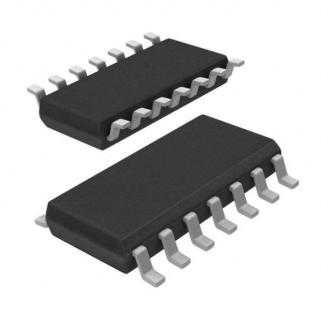
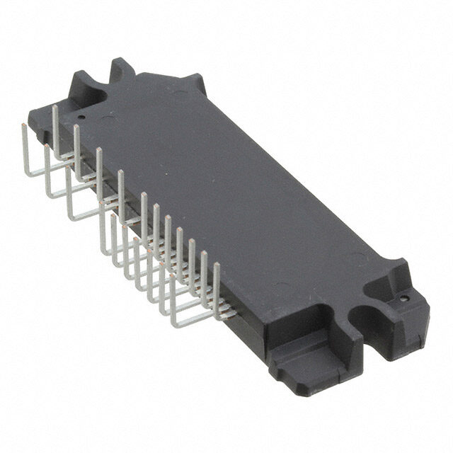
| 产品图片 |
|
| rohs | 符合RoHS无铅 / 符合限制有害物质指令(RoHS)规范要求 |
| 产品系列 | 电源管理 IC,马达/运动/点火控制器和驱动器,ON Semiconductor LB1836M-MPB-E- |
| 数据手册 | |
| 产品型号 | LB1836M-MPB-E |
| 产品 | Fan / Motor Controllers / Drivers |
| 产品培训模块 | http://www.digikey.cn/PTM/IndividualPTM.page?site=cn&lang=zhs&ptm=26174 |
| 产品种类 | 马达/运动/点火控制器和驱动器 |
| 供应商器件封装 | MFP14S |
| 其它名称 | LB1836M-MPB-E-ND |
| 功率耗散 | 800 mW |
| 功能 | 功率桥 - 逻辑驱动功率级 |
| 包装 | 带盒(TB) |
| 商标 | ON Semiconductor |
| 安装类型 | 表面贴装 |
| 安装风格 | SMD/SMT |
| 封装 | Bulk |
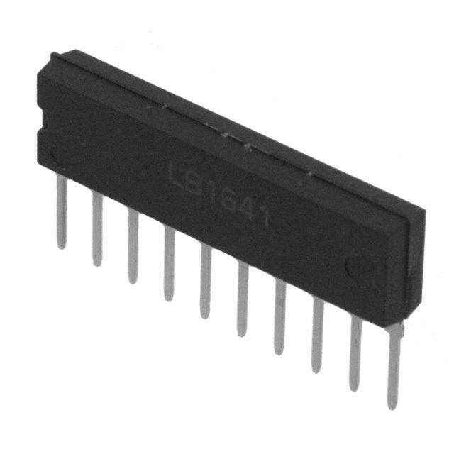
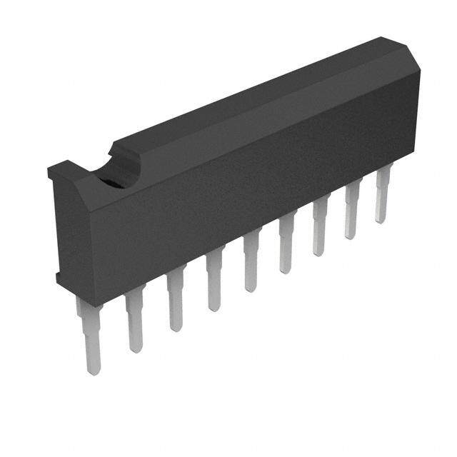
| 封装/外壳 | 14-LSOP(0.173",4.40mm 宽) |
| 封装/箱体 | MFP-14S |
| 工作温度 | -40°C ~ 85°C |
| 工作电源电压 | 2.5 V to 9 V |
| 工厂包装数量 | 60 |
| 应用 | 电池供电 |
| 接口 | 并联 |
| 标准包装 | 60 |
| 电压-电源 | 2.5 V ~ 9 V |
| 电压-负载 | 1.8 V ~ 9 V |
| 电机类型-AC,DC | - |
| 电机类型-步进 | 双极性 |
| 电流-输出 | 1A |
| 电源电流 | 10 uA |
| 类型 | Bidirectional Motor Driver |
| 系列 | LB1836M |
| 输出配置 | 全 H 桥,(2) 双 |


- 商务部:美国ITC正式对集成电路等产品启动337调查
- 曝三星4nm工艺存在良率问题 高通将骁龙8 Gen1或转产台积电
- 太阳诱电将投资9.5亿元在常州建新厂生产MLCC 预计2023年完工
- 英特尔发布欧洲新工厂建设计划 深化IDM 2.0 战略
- 台积电先进制程称霸业界 有大客户加持明年业绩稳了
- 达到5530亿美元!SIA预计今年全球半导体销售额将创下新高
- 英特尔拟将自动驾驶子公司Mobileye上市 估值或超500亿美元
- 三星加码芯片和SET,合并消费电子和移动部门,撤换高东真等 CEO
- 三星电子宣布重大人事变动 还合并消费电子和移动部门
- 海关总署:前11个月进口集成电路产品价值2.52万亿元 增长14.8%


PDF Datasheet 数据手册内容提取
Ordering number : EN3947F LB1836M M onolithic Digital IC L ow-Saturation Bidirectional Motor http://onsemi.com Driver for Low-Voltage Drive Overview The LB1836M is a low-saturation two-channel bidirectional motor driver IC for use in low-voltage applications. The LB1836M is a bipolar stepper-motor driver IC that is ideal for use in printers, FDDs, cameras and other portable devices. Features • Low voltage operation (2.5V min) • Low saturation voltage (upper transistor + lower transistor residual voltage ; 0.40V typ at 400mA). • Parallel connection (Upper transistor + lower transistor residual voltage ; 0.5V typ at 800mA). • Separate logic power supply and motor power supply • Brake function • Spark killer diodes built in • Thermal shutdown circuit built in • Compact package (14-pin MFP) Specifications Absolute Maximum Ratings at Ta = 25°C Parameter Symbol Conditions Ratings Unit Maximum supply voltage VCC max -0.3 to +10.5 V VS max -0.3 to +10.5 V Output supply voltage VOUT VS + VSF V Input supply voltage VIN -0.3 to +10 V GND pin flow-out current IGND Per channel 1.0 A Allowable power dissipation Pd max * Mounted on a board. 800 mW Operating temperature Topr -40 to +85 °C Storage temperature Tstg -55 to +150 °C * Mounted on a substrate: 30×30×1.5mm3, glass epoxy board. StressesexceedingMaximumRatingsmaydamagethedevice.MaximumRatingsarestressratingsonly.FunctionaloperationabovetheRecommendedOperating Conditions is not implied. Extended exposure to stresses above the Recommended Operating Conditions may affect device reliability. Semiconductor Components Industries, LLC, 2013 June, 2013 31110 SY/82207 MS/71807 MS 20070709-S00001/70407 MS PC/21097HA/D2293/O0693 No.3947-1/6
LB1836M Allowable Operating Ranges at Ta = 25°C Parameter Symbol Conditions Ratings Unit Supply voltage VCC 2.5 to 9.0 V VS 1.8 to 9.0 V Input “H”-level voltage VIH 1.8 to 9.0 V Input “L”-level voltage VIL -0.3 to +0.7 V Electrical Characteristics at Ta = 25°C, VCC = VS = 3V Ratings Parameter Symbol Conditions Unit min typ max Supply current ICC0 VIN1, 2, 3, 4 = 0V, ICC + IS 0.1 10 μA ICC1 VIN1 = 3V, VIN2, 3, 4 = 0V, ICC + IS 14 20 mA ICC2 VIN1, 2 = 3V, VIN3, 4 = 0V, ICC + IS 22 35 mA Output saturation voltage VOUT1 IOUT = 200mA 0.20 0.28 V (upper + lower) VOUT2 IOUT = 400mA 0.40 0.60 V VOUT3 IOUT = 400mA, Parallel connection 0.25 0.35 V VOUT4 IOUT = 800mA, Parallel connection 0.50 0.70 V Output sustain voltage VO (SUS) IOUT = 400mA 9 V Input current IIN VIN = 2V, VCC = 6V 80 μA Spark killer diode Reverse current IS (leak) VCC1, 2 = 9V 30 μA Forward voltage VSF IOUT = 400mA 1.7 V Package Dimensions unit : mm (typ) 3111A Pd max -- Ta W 1000 Specified board : 30×30×1.5mm3 m glass epoxy 14 8.0 8 ax -- 800 m d P 4.46.4 63 ation, 600 0. sip (1.0) 11.0 0.35 7 7MAX 0.15 wer dis 400 420 1. o (1.5) able p 200 0.1 Allow SANYO : MFP14S(225mil) 0 ñ 40 ñ 20 0 20 40 60 8085 100 Ambient temperature, Ta -- °C Pin Assignment GND IN3 OUT3 VS2 OUT4 IN4 Vcont 14 13 12 11 10 9 8 LB1836M 1 2 3 4 5 6 7 VCC IN1 OUT1 VS1 OUT2 IN2 GND Top view Note) Ground both GND pins. No.3947-2/6
LB1836M Block Diagram VCC VS2 VS1 10μF IN1 OUT1 er oll ontr M C OUT2 IN2 Thermal shutdown IN3 er OUT3 oll ontr M C OUT4 IN4 GND GND Truth Table IN1/3 IN2/4 OUT1/3 OUT2/4 Mode H L H L Forward L H L H Reverse H H L L Brake L L OFF OFF Standby No.3947-3/6
LB1836M Design Notes If large current flows on the power supply (VS) line and the GND line, then in some applications and layouts, misoperation due to line oscillation may result. The modes during which large current flows are as follows : • Motor surge current when the DC motor starts up or when it shifts rotation directions (forward ↔ reverse). • Passthrough current generated within the IC when shifting rotation directions (forward ↔ reverse) or when shifting from forward/reverse rotation to braking, or vice versa. The following points should be kept in mind regarding the pattern layout : • Keep the wiring lines thick and short in order to reduce wiring inductance between the power supply (VS) and GND. • Insert a passthrough capacitor near the IC. (Maximum effect is obtained by inserting the passthrough capacitor between VS and the pin 7 GND at the closest distance possible. • If the CPU and the LB1836M are mounted on separate boards and the difference between the ground potential of each board is large, install resistors of about 10kΩ in series between the CPU and the LB1836M inputs. Vcont pin VCC VS OUT M Ω ID OUT 0 IN 30 VZ ID = V rZ (= constant) Vcont As shown in the above diagram, the Vcont pin outputs the voltage of the band gap Zener VZ + VF (=1.93V). In normal use, this pin is left open. The drive current ID is varied by the Vcont voltage. However, because the band gap Zener is shared, it functions as a bridge. No.3947-4/6
LB1836M VO (sat) – IO IIN – Ta 1.0 110 VCC = VS = IN = 3V V – sat) 0.8 A 100 V (O μ– e, 0.6 N 90 on voltag 0.4 urrent, II 80 INI2N1 urati put c sat In ut 0.2 70 p ut O 0 0 0 100 200 300 400 500 600 – 40 – 20 0 20 40 60 80 100 120 140 160 Output current, IO – mA Ambient temperature, Ta – °C VO (sat) – Ta VO (sat) – IO 0.6 1.0 VCC = VS = IN = 3V V VO(sat) = total value V – 0.5 – at) at) 0.8 (sO 0.4 IO = 400mA (sO V V e, e, 0.6 g g saturation volta 00..32 IO = 200mA saturation volta 0.4 1ch totaPlarallel c o n n e ctio n total put 0.1 put 0.2 ut ut O O 0 0 – 40 – 20 0 20 40 60 80 100 120 140 0 100 200 300 400 500 600 700 800 900 Ambient temperature, Ta – °C Output current, IO – mA IS – Ta ICC – Ta 24 6 VCC = VS = IN = 3V VCC = VS = IN = 3V 20 5 A A m m Current drain, I–S 11268 RFeBovrrweearaskred urrent drain, I–CC 234 RFeovrBewrraseeradk C 4 1 0 0 – 40 – 20 0 20 40 60 80 100 120 140 160 – 40 – 20 0 20 40 60 80 100 120 140 160 Ambient temperature, Ta – °C Ambient temperature, Ta – °C IIN – VIN ICC – VCC 400 28 VCC = VS = 3V VS = IN = 3V IINN12 24 Break μA 300 IINN34 mA 20 – – Input current, IIN 120000 Current drain, ICC 11268 Forward/Reverse 4 Standby 0 0 0 1 2 3 4 5 6 7 8 9 10 0 1 2 3 4 5 6 7 8 9 10 11 Input voltage, VIN – V Supply voltage, VCC – V No.3947-5/6
LB1836M IS – VS 24 VCC = IN = 3V Break 20 A m 16 – S nt drain, I 12 Forward/Reverse urre 8 C 4 Standby 0 0 1 2 3 4 5 6 7 8 9 10 11 Supply voltage, VS – V ONSemiconductorandtheONlogoareregisteredtrademarksofSemiconductorComponentsIndustries,LLC(SCILLC).SCILLCownstherightstoanumber of patents, trademarks, copyrights, trade secrets, and other intellectual property. A listing of SCILLC’s product/patent coverage may be accessed at www.onsemi.com/site/pdf/Patent-Marking.pdf.SCILLCreservestherighttomakechangeswithoutfurthernoticetoanyproductsherein.SCILLCmakesno warranty,representationorguaranteeregardingthesuitabilityofitsproductsforanyparticularpurpose,nordoesSCILLCassumeanyliabilityarisingoutofthe applicationoruseofanyproductorcircuit,andspecificallydisclaimsanyandallliability,includingwithoutlimitationspecial,consequentialorincidental damages.“Typical”parameterswhichmaybeprovidedinSCILLCdatasheetsand/orspecificationscananddovaryindifferentapplicationsandactual performancemayvaryovertime.Alloperatingparameters,including“Typicals” mustbevalidatedforeachcustomerapplicationbycustomer’stechnical experts.SCILLCdoesnotconveyanylicenseunderitspatentrightsnortherightsofothers.SCILLCproductsarenotdesigned,intended,orauthorizedforuse ascomponentsinsystemsintendedforsurgicalimplantintothebody,orotherapplicationsintendedtosupportorsustainlife,orforanyotherapplicationin whichthefailureoftheSCILLCproductcouldcreateasituationwherepersonalinjuryordeathmayoccur.ShouldBuyerpurchaseoruseSCILLCproductsfor anysuchunintendedorunauthorizedapplication,BuyershallindemnifyandholdSCILLCanditsofficers,employees,subsidiaries,affiliates,anddistributors harmlessagainstallclaims,costs,damages,andexpenses,andreasonableattorneyfeesarisingoutof,directlyorindirectly,anyclaimofpersonalinjuryor deathassociatedwithsuchunintendedorunauthorizeduse,evenifsuchclaimallegesthatSCILLCwasnegligentregardingthedesignormanufactureofthe part. SCILLC is an Equal Opportunity/Affirmative Action Employer. This literature is subject to all applicable copyright laws and is not for resale in any manner. PS No.3947-6/6