ICGOO在线商城 > 集成电路(IC) > PMIC - 全,半桥驱动器 > FDMF5822DC

 Datasheet下载
- 型号: FDMF5822DC
- 制造商: Fairchild Semiconductor
- 库位|库存: xxxx|xxxx
- 要求:
| 数量阶梯 | 香港交货 | 国内含税 |
| +xxxx | $xxxx | ¥xxxx |
查看当月历史价格
查看今年历史价格
FDMF5822DC产品简介:
ICGOO电子元器件商城为您提供FDMF5822DC由Fairchild Semiconductor设计生产,在icgoo商城现货销售,并且可以通过原厂、代理商等渠道进行代购。 FDMF5822DC价格参考。Fairchild SemiconductorFDMF5822DC封装/规格:PMIC - 全,半桥驱动器, Half Bridge Driver Synchronous Buck Converters UMOS 31-PQFN (5x5)。您可以下载FDMF5822DC参考资料、Datasheet数据手册功能说明书,资料中有FDMF5822DC 详细功能的应用电路图电压和使用方法及教程。
FDMF5822DC是安森美(ON Semiconductor)推出的一款高度集成的PMIC模块,属于全桥/半桥驱动器类别,主要面向高性能、高效率的电源管理应用。该器件集成了驱动器IC与功率MOSFET,适用于空间受限但要求高功率密度的设计。

其典型应用场景包括:

1. 服务器和数据中心电源系统:FDMF5822DC具备高效能和低热阻特性,适用于服务器主板上的多相电压调节模块(VRM),为CPU、GPU或ASIC等高性能处理器提供稳定、精确的供电。

2. 通信基础设施设备:在5G基站、网络交换机和路由器中,该器件可用于负载点(POL)电源转换,满足高频开关和高可靠性的需求。

3. 工业自动化与高端计算设备:适用于需要紧凑型电源设计的工业控制板、FPGA供电及嵌入式计算平台,提供良好的动态响应和负载调整能力。

4. 高密度DC-DC转换器:得益于其小型化封装(如Power integrate™ DrMOS模块),适合用于大电流、低电压输出的同步整流拓扑结构,提升整体转换效率并降低系统温升。

FDMF5822DC通过优化的栅极驱动设计和集成保护功能(如过温、过流保护),增强了系统的稳定性与安全性,广泛应用于对能效、尺寸和可靠性有严苛要求的现代电子系统中。
| 参数 | 数值 |
| 产品目录 | 集成电路 (IC)半导体 |
| 描述 | MOD SMART PWR STAGE 2MHZ 31MLP门驱动器 Smart Power Stage (SPS) Module with Integrated Thermal Warning and Thermal Shutdown |
| 产品分类 | PMIC - MOSFET,电桥驱动器 - 内部开关集成电路 - IC |
| 品牌 | Fairchild Semiconductor |
| 产品手册 | |
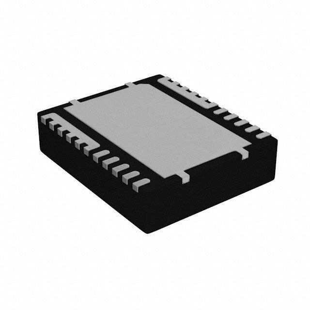
| 产品图片 |
|
| rohs | 符合RoHS无铅 / 符合限制有害物质指令(RoHS)规范要求 |
| 产品系列 | 电源管理 IC,门驱动器,Fairchild Semiconductor FDMF5822DC- |
| 数据手册 | |
| 产品型号 | FDMF5822DC |
| 上升时间 | 4 ns |
| 下降时间 | 3 ns |
| 产品 | MOSFET Gate Drivers |
| 产品种类 | 门驱动器 |
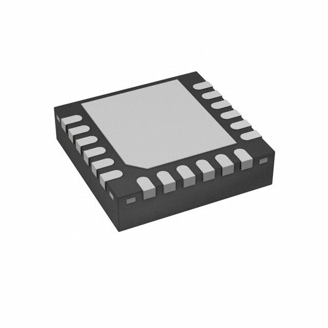
| 供应商器件封装 | 31-PQFN (5x5) |
| 其它名称 | FDMF5822DCDKR |
| 包装 | Digi-Reel® |
| 单位重量 | 257.194 mg |
| 商标 | Fairchild Semiconductor |
| 安装类型 | 表面贴装 |
| 安装风格 | SMD/SMT |
| 导通电阻 | - |
| 封装 | Reel |
| 封装/外壳 | 31-PowerWFQFN |
| 封装/箱体 | PQFN-31 |
| 工作温度 | -40°C ~ 125°C |
| 工厂包装数量 | 3000 |
| 最大工作温度 | + 125 C |
| 最小工作温度 | - 40 C |
| 标准包装 | 1 |
| 激励器数量 | 2 Driver |
| 特色产品 | http://www.digikey.cn/product-highlights/cn/zh/fairchild-cloud-systems-computing/4301 |
| 电压-电源 | 4.5 V ~ 16 V |
| 电流-峰值输出 | - |
| 电流-输出/通道 | 55A |
| 电源电压-最大 | 5.5 V |
| 电源电压-最小 | 4.5 V |
| 电源电流 | 2 mA |
| 类型 | 半桥 |
| 系列 | FDMF5822DC |
| 输入类型 | PWM |
| 输出数 | 1 |
| 输出电流 | 55 A |
| 输出端数量 | 1 |
| 配置 | Non-Inverting |


- 商务部:美国ITC正式对集成电路等产品启动337调查
- 曝三星4nm工艺存在良率问题 高通将骁龙8 Gen1或转产台积电
- 太阳诱电将投资9.5亿元在常州建新厂生产MLCC 预计2023年完工
- 英特尔发布欧洲新工厂建设计划 深化IDM 2.0 战略
- 台积电先进制程称霸业界 有大客户加持明年业绩稳了
- 达到5530亿美元!SIA预计今年全球半导体销售额将创下新高
- 英特尔拟将自动驾驶子公司Mobileye上市 估值或超500亿美元
- 三星加码芯片和SET,合并消费电子和移动部门,撤换高东真等 CEO
- 三星电子宣布重大人事变动 还合并消费电子和移动部门
- 海关总署:前11个月进口集成电路产品价值2.52万亿元 增长14.8%


PDF Datasheet 数据手册内容提取
Is Now Part of To learn more about ON Semiconductor, please visit our website at www.onsemi.com Please note: As part of the Fairchild Semiconductor integration, some of the Fairchild orderable part numbers will need to change in order to meet ON Semiconductor’s system requirements. Since the ON Semiconductor product management systems do not have the ability to manage part nomenclature that utilizes an underscore (_), the underscore (_) in the Fairchild part numbers will be changed to a dash (-). This document may contain device numbers with an underscore (_). Please check the ON Semiconductor website to verify the updated device numbers. The most current and up-to-date ordering information can be found at www.onsemi.com. Please email any questions regarding the system integration to Fairchild_questions@onsemi.com. ON Semiconductor and the ON Semiconductor logo are trademarks of Semiconductor Components Industries, LLC dba ON Semiconductor or its subsidiaries in the United States and/or other countries. ON Semiconductor owns the rights to a number of patents, trademarks, copyrights, trade secrets, and other intellectual property. A listing of ON Semiconductor’s product/patent coverage may be accessed at www.onsemi.com/site/pdf/Patent-Marking.pdf. ON Semiconductor reserves the right to make changes without further notice to any products herein. ON Semiconductor makes no warranty, representation or guarantee regarding the suitability of its products for any particular purpose, nor does ON Semiconductor assume any liability arising out of the application or use of any product or circuit, and specifically disclaims any and all liability, including without limitation special, consequential or incidental damages. Buyer is responsible for its products and applications using ON Semiconductor products, including compliance with all laws, regulations and safety requirements or standards, regardless of any support or applications information provided by ON Semiconductor. “Typical” parameters which may be provided in ON Semiconductor data sheets and/or specifications can and do vary in different applications and actual performance may vary over time. All operating parameters, including “Typicals” must be validated for each customer application by customer’s technical experts. ON Semiconductor does not convey any license under its patent rights nor the rights of others. ON Semiconductor products are not designed, intended, or authorized for use as a critical component in life support systems or any FDA Class 3 medical devices or medical devices with a same or similar classification in a foreign jurisdiction or any devices intended for implantation in the human body. Should Buyer purchase or use ON Semiconductor products for any such unintended or unauthorized application, Buyer shall indemnify and hold ON Semiconductor and its officers, employees, subsidiaries, affiliates, and distributors harmless against all claims, costs, damages, and expenses, and reasonable attorney fees arising out of, directly or indirectly, any claim of personal injury or death associated with such unintended or unauthorized use, even if such claim alleges that ON Semiconductor was negligent regarding the design or manufacture of the part. ON Semiconductor is an Equal Opportunity/Affirmative Action Employer. This literature is subject to all applicable copyright laws and is not for resale in any manner.
F D M F May 2016 5 8 2 2 D C FDMF5822DC – Smart Power Stage (SPS) Module — with Integrated Thermal Warning and Thermal Shutdown S m a r Features Description t P Ultra-Compact 5 mm x 5 mm PQFN Copper-Clip The SPS family is Fairchild’s next-generation, fully o w Package with Flip Chip Low-Side MOSFET and optimized, ultra-compact, integrated MOSFET plus e Dual Cool Architecture driver power stage solution for high-current, high- r frequency, synchronous buck, DC-DC applications. The S High Current Handling: 55 A FDMF5822DC integrates a driver IC with a bootstrap ta 3-State 3.3 V PWM Input Gate Driver Schottky diode, two power MOSFETs, and a thermal ge monitor into a thermally enhanced, ultra-compact 5 mm, Dynamic Resistance Mode for Low-Side Drive x 5 mm package. (S (LDRV) Slows Low-Side MOSFET during Negative P Inductor Current Switching With an integrated approach, the SPS switching power S ) Auto DCM (Low-Side Gate Turn Off) Using spteargfoer misa nocpet,i mmizineimd izfoerd dsryisvteerm a inndd uMctOanScFeE, Ta nddy pnoawmeicr Mo ZCD# Input MOSFET R . The SPS family uses Fairchild's high- d DS(ON) Thermal Warning (THWN#) to Warn Over- performance PowerTrench® MOSFET technology, ul e Temperature of Gate Driver IC which reduces switch ringing, eliminating the need for a w snubber circuit in most buck converter applications. Thermal Shutdown (THDN) it h A driver IC with reduced dead times and propagation HS-Short Detect Fault# / Shutdown I delays further enhances the performance. A thermal n Dual Mode Enable / Fault# Pin warning function warns of a potential over-temperature te situation. A thermal shutdown function turns off the g Internal Pull-Up and Pull-Down for ZCD# and driver if an over-temperature condition occurs. The ra EN Inputs, respectively FDMF5822DC incorporates an Auto-DCM Mode (ZCD#) te d Fairchild PowerTrench® MOSFETs for Clean for improved light-load efficiency. The FDMF5822DC T Voltage Waveforms and Reduced Ringing also provides a 3-state 3.3 V PWM input for h compatibility with a wide range of PWM controllers. e Fairchild SyncFET™ Technology (Integrated r m Schottky Diode) in Low-Side MOSFET Applications a Integrated Bootstrap Schottky Diode l W Optimized / Extremely Short Dead-Times Servers and Workstations, V-Core and Non-V-Core a DC-DC Converters r n Under-Voltage Lockout (UVLO) on VCC Desktop and All-in-One Computers, V-Core and in Optimized for Switching Frequencies up to 1.5 MHz Non-V-Core DC-DC Converters g a PWM Minimum Controllable On-Time: 30 ns High-Performance Gaming Motherboards n d Low Shutdown Current: < 3 µA High-Current DC-DC Point-of-Load Converters T h Optimized FET Pair for Highest Efficiency: Networking and Telecom Microprocessor Voltage e r 10 ~ 15% Duty Cycle Regulators m a Operating Junction Temperature Range: Small Form-Factor Voltage Regulator Modules l -40°C to +125°C S h Fairchild Green Packaging and RoHS Compliance u t d o w Ordering Information n Part Number Current Rating Package Top Mark FDMF5822DC 55 A 31-Lead, Clip Bond PQFN SPS, 5.0 mm x 5.0 mm Package 5822DC © 2013 Fairchild Semiconductor Corporation www.fairchildsemi.com FDMF5822DC • Rev. 1.9
Application Diagram F D V V M 5V IN CPVCC RVCC CVCC CVIN F58 2 2 D PVCC VCC VIN C — EN EN/FAULT# GL S R m BOOT a PWM Input PWM BOOT r t FDMF5822DC C P OFF BOOT o ON ZCD# PHASE w L e OUT r THWN# THWN# SW VOUT S t a g AGND PGND C e OUT ( S P S Figure 1. Typical Application Diagram ) M Functional Block Diagram o d u FAEUNL/T# PVCC BOOT VIN le w i t h THWN# I n t e g r a 0.8V/2.0V t FAULT e VCC LATCH d T h THWN / e THDN rm FAULT PHASE a l W a VCC LEVEL rn EN/UVLO HDRV SHIFT i n g POR a n RUP_PWM SW d PWM CONTROL PVCC T PWM PWM INPUT LOGIC h e RDN_PWM LDRV1 r m a l VCC POR PVCC S h LDRV2 GL u ↓ 10uA td o ZCD# ZCD/CCM/DCM w LOGIC n 0.8V/2.0V AGND PGND Figure 2. Functional Block Diagram © 2013 Fairchild Semiconductor Corporation www.fairchildsemi.com FDMF5822DC • Rev. 1.9 2
F D M Pin Configuration F 5 8 7 6 5 4 3 2 1 VIN PHASE NC BOOT AGND VCC ZCD# PWM 822 D 8 7 6 5 4 3 2 1 C EN/ — 9 31 VIN 9 31 FAULT# S 10 30 VIN 10 30 THWN# m 32 AGND a 11 29 VIN 11 29 PVCC rt P 28 28 PGND o w 33 e 12 27 PGND 12 GL 27 GL r S 13 26 PGND 13 26 SW ta g 14 25 PGND 14 25 SW e ( S 15 24 PGND 15 24 SW P S 16 17 18 19 20 21 22 23 ) M 16 17 18 19 20 21 22 23 W W W W W W W W S S S S S S S S o d Figure 3. Pin Configuration - Top View and Transparent View u l e w i Pin Definitions t h I n Pin # Name Description t e g 1 PWM PWM input to the gate driver IC r a 2 ZCD# Enable input for the ZCD (Auto DCM) comparator t e d 3 VCC Power supply input for all analog control functions; this is the “quiet” VCC T 4, 32 AGND Analog ground for analog portions of the IC and for substrate, internally tied to PGND h e 5 BOOT Supply for the high-side MOSFET gate driver. A capacitor from BOOT to PHASE supplies rm the charge to turn on the N-channel high-side MOSFET a l 6 NC No connect W 7 PHASE Return connection for the boot capacitor, internally tied to SW node a r n 8~11 VIN Power input for the power stage i n 12~15, 28 PGND Power return for the power stage g a Switching node junction between high-side and low-side MOSFETs; also input to the gate n 16~26 SW d driver SW node comparator and input into the ZCD comparator T 27, 33 GL Gate Low, Low-side MOSFET gate monitor h e 29 PVCC Power supply input for LS(1) gate driver and boot diode r m 125°C Thermal Warning Flag – pulls LOW upon detection of 125°C thermal warning pre- a 30 THWN# l set temperature S h Dual-functionality, enable input to the gate driver IC. FAULT# - internal pull-down 31 EN / physically pulls this pin LOW upon detection of fault condition (HS(2) MOSFET short or ut FAULT# d 150°C THDN) o w Notes: n 1. LS = Low Side. 2. HS = High Side. © 2013 Fairchild Semiconductor Corporation www.fairchildsemi.com FDMF5822DC • Rev. 1.9 3
F Absolute Maximum Ratings D Stresses exceeding the Absolute Maximum Ratings may damage the device. The device may not function or be M F operable above the recommended operating conditions and stressing the parts to these levels is not recommended. 5 In addition, extended exposure to stresses above the recommended operating conditions may affect device reliability. 8 2 The absolute maximum ratings are stress ratings only. T = T = 25°C. A J 2 D Symbol Parameter Min. Max. Unit C V Supply Voltage Referenced to AGND -0.3 6.0 V — CC PVCC Drive Voltage Referenced to AGND -0.3 6.0 V S m V Output Enable / Disable Referenced to AGND -0.3 6.0 V EN/FAULT# a VPWM PWM Signal Input Referenced to AGND -0.3 VCC+0.3 V rt P VZCD# ZCD Mode Input Referenced to AGND -0.3 6.0 V o w Low Gate Manufacturing Test Referenced to AGND (DC only) -0.3 6.0 V V e GL Pin Referenced to AGND AC<20 nS -3.0 6.0 r S V Thermal Warning Referenced to AGND -0.3 6.0 V t THWN# a g V Power Input Referenced to PGND, AGND -0.3 25.0 V IN e Referenced to PGND, AGND (DC Only) -0.3 25.0 ( S V PHASE V PHASE P Referenced to PGND, AC < 20 ns -7.0 30.0 S Referenced to PGND, AGND (DC Only) -0.3 25.0 ) V Switch Node Input V M SW Referenced to PGND, AC < 20 ns -7.0 30.0 o d Referenced to AGND (DC Only) -0.3 30.0 u VBOOT Bootstrap Supply Referenced to AGND, AC < 20 ns -5.0 35.0 V le w V Boot to PHASE Voltage Referenced to PVCC -0.3 6.0 V BOOT-PHASE i t h f =300 kHz, V =12 V, V =1.8 V 55 IO(AV)(3) Output Current SW IN OUT A In f =1 MHz, V =12 V, V =1.8 V 50 SW IN OUT t e IFAULT EN / FAULT# Sink Current -0.1 7.0 mA g r θ Junction-to-Ambient Thermal Resistance 12.4 °C/W a J-A t e θJ-PCB Junction-to-PCB Thermal Resistance (under Fairchild SPS Thermal Board) 1.8 °C/W d T Ambient Temperature Range -40 +125 °C T A h T Maximum Junction Temperature +150 °C e J r m T Storage Temperature Range -55 +150 °C STG a Human Body Model, ANSI/ESDA/JEDEC l ESD Electrostatic Discharge JS-001-2012 3000 V W Protection a Charged Device Model, JESD22-C101 2500 r n Note: in 3. I is rated with testing Fairchild’s SPS evaluation board at T = 25°C with natural convection cooling. This g O(AV) A rating is limited by the peak SPS temperature, T = 150°C, and varies depending on operating conditions and a J n PCB layout. This rating may be changed with different application settings. d Recommended Operating Conditions T h The Recommended Operating Conditions table defines the conditions for actual device operation. Recommended e r Operating Conditions are specified to ensure optimal performance to the datasheet specifications. Fairchild does not m recommend exceeding them or designing to Absolute Maximum Ratings. a l S Symbol Parameter Min. Typ. Max. Unit h u VCC Control Circuit Supply Voltage 4.5 5.0 5.5 V td PV Gate Drive Circuit Supply Voltage 4.5 5.0 5.5 V o CC w VIN Output Stage Supply Voltage 4.5(4) 12.0 16.0(5) V n T Operating Junction Temperature -40 +125 °C J Notes: 4. 3.0 V V is possible according to the application condition. IN 5. Operating at high V can create excessive AC voltage overshoots on the SW-to-GND and BOOT-to-GND nodes during IN MOSFET switching transient. For reliable SPS operation, SW to GND and BOOT to GND must remain at or below the Absolute Maximum Ratings in the table above. © 2013 Fairchild Semiconductor Corporation www.fairchildsemi.com FDMF5822DC • Rev. 1.9 4
F Electrical Characteristics D M Typical value is under V =12 V, V =PV =5 V and T =T=+ 25°C unless otherwise noted. Minimum / Maximum IN CC CC A J F values are under VIN=12 V, VCC=PVCC=5 V ± 10% and TJ=TA=-40 ~ 125°C unless otherwise noted. 5 8 Symbol Parameter Condition Min. Typ. Max. Unit 2 2 Basic Operation D C I Quiescent Current IQ=IVCC + IPVCC, EN=HIGH, PWM=LOW or 2 mA — Q HIGH or Float (Non-Switching) S I Shutdown Current I =I + I , EN=GND 3 µA SHDN SHDN VCC PVCC m VUVLO UVLO Threshold VCC Rising 3.5 3.8 4.1 V a r V UVLO Hysteresis 0.4 V t UVLO_HYST P tD_POR POR Delay to Enable IC VCC UVLO Rising to Internal PWM Enable 20 µs o w EN Input e V High-Level Input Voltage 2.0 V r IH_EN S VIL_EN Low-Level Input Voltage 0.8 V ta R Pull-Down Resistance 250 kΩ g PLD_EN e tPD_ENL EN LOW Propagation Delay PLOWWM =GND, EN Going LOW to GL Going 25 ns (S P PWM=GND, EN Going HIGH to GL S tPD_ENH EN HIGH Propagation Delay Going HIGH 20 µs ) M ZCD# Input o d VIH_ZCD# High-Level Input Voltage 2.0 V u l V Low-Level Input Voltage 0.8 V e IL_ZCD# w I Pull-Up Current 10 µA PLU_ZCD# i t PWM=GND, ZCD# Going LOW to GL h tPD_ZLGLL ZCD# LOW Propagation Delay Going LOW (assume IL <=0) 10 ns In t ZCD# HIGH Propagation Delay PWM=GND, ZCD# Going HIGH to GL 10 ns te PD_ZHGLH Going HIGH g r PWM Input a t e RUP_PWM Pull-Up Impedance 23 kΩ d R Pull-Down Impedance 10 kΩ T DN_PWM Typical Values: T =T=25°C, h VIH_PWM PWM High Level Voltage V =PV =5 V, A J 2.2 V e CC CC r V 3-State Window Min. / Max. Values: 1.2 1.8 V m TRI_Window T =T=-40°C to 125°C, a VIL_PWM PWM Low Level Voltage VA =PJV =5 V ±10% 0.8 V l CC CC W t 3-State Shut-Off Time 90 130 ns D_HOLD-OFF a VHIZ_PWM 3-State Open Voltage 1.3 1.5 1.7 V rn Minimum Controllable On-Time in g PWM Minimum Controllable On- Minimum PWM HIGH Pulse Required for tMIN_PWM_ON Time SW Node to Switch from GND to VIN 30 ns a n Forced Minimum GL HIGH Time d T Minimum GL HIGH Time when LOW h t Forced Minimum GL HIGH V detected and PWM 100 ns e MIN_GL_HIGH BOOT-SW r LOW=<100 ns m PWM Propagation Delays & Dead Times (V =12 V, V =PV =5 V, f =1 MHz, I =20 A, T =25°C) a IN CC CC SW OUT A l PWM Going HIGH to GL Going LOW, S tPD_PHGLL PWM HIGH Propagation Delay V to 90% GL 15 ns h IH_PWM u PWM Going LOW to GH(6) Going LOW, td t PWM LOW Propagation Delay 30 ns PD_PLGHL V to 90% GH o IL_PWM w PWM HIGH Propagation Delay PWM Going HIGH to GH Going HIGH, n t V to 10% GH (ZCD#=LOW, I =0, 10 ns PD_PHGHH (ZCD# Held LOW) IH_PWM L Assumes DCM) Continued on the following page… © 2013 Fairchild Semiconductor Corporation www.fairchildsemi.com FDMF5822DC • Rev. 1.9 5
F Electrical Characteristics D M Typical value is under V =12 V, V =PV =5 V and T =T=+ 25°C unless otherwise noted. Minimum / Maximum IN CC CC A J F values are under VIN=12 V, VCC=PVCC=5 V ± 10% and TJ=TA=-40 ~ 125°C unless otherwise noted. 5 8 Symbol Parameter Condition Min. Typ. Max. Unit 2 2 GL Going LOW to GH Going HIGH, 10% D C t LS Off to HS On Dead Time GL to 10% GH, PWM Transition LOW to 10 ns D_DEADON HIGH – See Figure 27 — GH Going LOW to GL Going HIGH, 10% S t HS Off to LS On Dead Time GH to 10% GL, PWM Transition HIGH to 5 ns m D_DEADOFF LOW – See Figure 27 a r t GH Rise Time under 20 A I 10% GH to 90% GH, I =20 A 9 ns t R_GH_20A OUT OUT P tF_GH_20A GH Fall Time under 20 A IOUT 90% GH to 10% GH, IOUT=20 A 9 ns o w t GL Rise Time under 20 A I 10% GL to 90% GL, I =20 A 9 ns R_GL_20A OUT OUT e t GL Fall Time under 20 A I 90% GL to 10% GL, I =20 A 6 ns r F_GL_20A OUT OUT S Exiting 3-State Propagation PWM (from 3-State) Going HIGH to GH tPD_TSGHH Delay Going HIGH, V to 10% GH 45 ns ta IH_PWM g Exiting 3-State Propagation PWM (from 3-State) Going LOW to GL e tPD_TSGLH Delay Going HIGH, V to 10% GL 45 ns ( IL_PWM S High-Side Driver (HDRV, V = PV = 5 V) P CC CC S RSOURCE_GH Output Impedance, Sourcing Source Current=100 mA 0.68 Ω ) M R Output Impedance, Sinking Sink Current=100 mA 0.9 Ω SINK_GH o tR_GH GH Rise Time 10% GH to 90% GH, CLOAD=1.3 nF 4 ns d u tF_GH GH Fall Time 90% GH to 10% GH, CLOAD=1.3 nF 3 ns le Weak Low-Side Driver (LDRV2 Only under CCM2 Mode Operation, V = PV = 5 V) CC CC w RSOURCE_GL Output Impedance, Sourcing Source Current=100 mA 0.82 Ω it h ISOURCE_GL Output Sourcing Peak Current GL=2.5 V 2 A I n RSINK_GL Output Impedance, Sinking Sink Current=100 mA 0.86 Ω t e ISINK_GL Output Sinking Peak Current GL=2.5 V 2 A g r Low-Side Driver (Paralleled LDRV1 + LDRV2 under CCM1 Mode Operation, V = PV = 5 V) a CC CC t R Output Impedance, Sourcing Source Current=100 mA 0.47 Ω e SOURCE_GL d ISOURCE_GL Output Sourcing Peak Current GL=2.5 V 4 A T h R Output Impedance, Sinking Sink Current=100 mA 0.29 Ω SINK_GL e ISINK_GL Output Sinking Peak Current GL=2.5 V 7 A rm tR_GL GL Rise Time 10% GL to 90% GL, CLOAD=7.0 nF 9 ns a l tF_GL GL Fall Time 90% GL to 10% GL, CLOAD=7.0 nF 6 ns W Thermal Monitor Current a r I Thermal Monitor Current T =T=25°C 39.3 40.2 41.0 µA n TMON_25 A J i n I Thermal Monitor Current T =T=150°C 58 µA TMON_150 A J g Thermal Warning Flag (125°C) a n TACT_THWN_125 Activation Temperature 125 °C d Measured on the driver IC with T=T J A T Reset Temperature 110 °C T RST_THWN_125 h RPLD_THWN Pull-Down Resistance IPLD_THWN=1 mA 100 Ω e r Thermal Shutdown (150°C) m T Activation Temperature Measured on the driver IC with T=T 150 °C a ACT_THDN J A l R Pull-Down Resistance I =1 mA 50 Ω S PLD_EN-THDN PLD_EN-THDN h Catastrophic Fault (SW Monitor) u t V SW Monitor Reference Voltage 1.3 2 V d SW_MON o Propagation Delay to Pull EN / w t 20 ns D_FAULT FAULT# Signal = LOW n Boot Diode V Forward-Voltage Drop I =10 mA 0.4 V F F V Breakdown Voltage I =1 mA 30 V R R Note: 6 . GH = Gate High, internal gate pin of the high-side MOSFET. © 2013 Fairchild Semiconductor Corporation www.fairchildsemi.com FDMF5822DC • Rev. 1.9 6
F D Typical Performance Characteristics M F Test Conditions: VIN=12 V, VCC=PVCC=5 V, VOUT=1.8 V, LOUT=250 nH, TA=25°C and natural convection cooling, 5 unless otherwise noted. 8 2 2 60 12 D 55 11 12Vin, 300kHz C 12Vin, 500kHz 50 10 — Output Current, I[A]OUT 223344050505 FSW=F S3W00=k 1H0z00kHz Power Loss, PL[W]MOD 456789 1122VViinn,, 810000k0HkHzz Smart Pow ule 15 ule 3 er d d o 10 o 2 S M M t 5 VIN= 12V, PVCC& VCC= 5V, VOUT= 1.8V 1 PVCC& VCC= 5V, VOUT= 1.8V a g 0 0 e 0 25 50 75 100 125 150 0 5 10 15 20 25 30 35 40 45 50 55 60 PCB Temperature, TPCB[ C] Module Output Current, IOUT[A] (S P S Figure 4. Safe Operating Area Figure 5. Power Loss vs. Output Current ) M 1.4 1.12 o VIN= 12V, PVCC& VCC= 5V, VOUT= 1.8V, IOUT= 30A PVCC& VVCC= 5V, VOUT= 1.8V, FSW= 500kHz, IOUT= 30A d 1.10 u s1.3 ss le ower Los1.2 Power Lo11..0068 with ule P1.1 dule 1.04 In d o t o M e ed M1.0 zed 1.02 gr ormaliz0.9 Normali1.00 ated N 0.98 T 0.8 0.96 h e 200 300 400 500 600 700 800 900 1000 1100 4 6 8 10 12 14 16 18 r Module Switching Frequency, FSW [kHz] Module Input Voltage, VIN [V] m a l Figure 6. Power Loss vs. Switching Frequency Figure 7. Power Loss vs. Input Voltage W a 1.10 1.5 r n VIN= 12V, VOUT= 1.8V, FSW= 500kHz, IOUT= 30A VIN= 12V, PVCC& VVCC= 5V, FSW= 500kHz, IOUT= 30A i n 1.08 malized Module Power Loss01111.....9000080462 malized Module Power Loss1111....1234 g and Thermal S Nor0.96 Nor1.0 hu t d 0.94 0.9 o 4.0 4.5 5.0 5.5 6.0 0.5 1.0 1.5 2.0 2.5 3.0 3.5 w Driver Supply Voltage, PVCC & VCC [V] Module Output Voltage, VOUT [V] n Figure 8. Power Loss vs. Driver Supply Voltage Figure 9. Power Loss vs. Output Voltage © 2013 Fairchild Semiconductor Corporation www.fairchildsemi.com FDMF5822DC • Rev. 1.9 7
F D Typical Performance Characteristics M F Test Conditions: VIN=12 V, VCC=PVCC=5 V, VOUT=1.8 V, LOUT=250 nH, TA=25°C and natural convection cooling, 5 unless otherwise noted. 8 2 2 1.010 0.05 D VIN= 12V, PVCC& VVCC= 5V, FSW= 500kHz, VOUT= 1.8V, IOUT= 30A VIN= 12V, PVCC& VCC= 5V, VOUT= 1.8V, IOUT= 0A C A] — er Loss1.000 + I[VCC0.04 Sm w C ed Module Po00..998900 y Current, IPVC0.03 art Pow Normaliz0.970 Driver Suppl 0.02 er Sta g 0.960 0.01 e 200 250 300 350 400 450 500 200 300 400 500 600 700 800 900 1000 1100 ( Output Inductor, LOUT [nH] Module Switching Frequency, FSW [kHz] S P S Figure 10. Power Loss vs. Output Inductor Figure 11. Driver Supply Current vs. Switching ) Frequency M o 0.026 1.10 d VIN= 12V, VOUT= 1.8V, FSW= 500kHz, IOUT= 0A 1.08 VIN= 12V, PVCC& VVCC= 5V, VOUT= 1.8V ul e A] 1.06 + I[VCC0.024 Current11..0024 FSW= 1000kHz with nt, IPVCC0.022 Supply 01..9080 Inte Driver Supply Curre00.0.0128 Normalized Driver 00000.....8999982460 FSW= 300kHz grated The 0.016 0.86 r m 4.0 4.5 5.0 5.5 6.0 0 5 10 15 20 25 30 35 40 45 50 55 60 Driver Supply Voltage, PVCC & VVCC [V] Module Output Current, IOUT[A] al W Figure 12. Driver Supply Current vs. Driver Supply Figure 13. Driver Supply Current vs. Output Current a r Voltage n i n 4.0 2.2 g UVLOUP TA= 25°C VIH_PWM a 3.9 2.0 n er Supply Voltage, V[V]CC 3333....6785 hreshold Voltage, V[V]PWM1111....2684 VVHITZR_IP_WHIM d Thermal Shu Driv 3.4 UVLODN PWM T 1.0 VTRI_LO tdo VIL_PWM w 3.3 0.8 n -55 0 25 55 100 125 4.50 4.75 5.00 5.25 5.50 Driver IC Junction Temperature, TJ[oC] Driver Supply Voltage, VCC [V] Figure 14. UVLO Threshold vs. Temperature Figure 15. PWM Threshold vs. Driver Supply Voltage © 2013 Fairchild Semiconductor Corporation www.fairchildsemi.com FDMF5822DC • Rev. 1.9 8
F D M Typical Performance Characteristics F 5 Test Conditions: V =12 V, V =PV =5 V, V =1.8 V, L =250 nH, T =25°C and natural convection cooling, 8 IN CC CC OUT OUT A 2 unless otherwise noted. 2 D 2.2 1.8 C VCC= 5V VIH_PWM TA= 25°C — PWM Threshold Voltage, V[V]PWM111112......024680 VVHVTITZRR_IP_I_WHLIOM ZCD# Threshold Voltage, V[V]ZCD#1111111.......1235674 VVIIHL__ZZCCDD## Smart Power Stag VIL_PWM e 0.8 1.0 ( -55 0 25 55 100 125 4.50 4.75 5.00 5.25 5.50 S Driver IC Junction Temperature, TJ[oC] Driver Supply Voltage, VCC [V] PS ) Figure 16. PWM Threshold vs. Temperature Figure 17. ZCD# Threshold vs. Driver Supply M Voltage o d u 2 0.22 1.9 VCC= 5V VCC= 5V le w D# Threshold Voltage, V[V]ZCD#1111111.......2346785 VIH_ZCD# ZCD# Pull-Up Current, I[uA]PLU00000....1111.22468 ith Integrated Th ZC 1.1 VIL_ZCD# e r 1 0.1 m -55 0 25 55 100 125 -55 0 25 55 100 125 a l Driver IC Junction Temperature, TJ[oC] Driver IC Junction Temperature, TJ[oC] W a r Figure 18. ZCD# Threshold vs. Temperature Figure 19. ZCD# Pull-Up Current vs. Temperature n i n 2.2 2.0 g TA= 25°C 1.9 VCC = 5V a n 2.0 VIH_EN 1.8 d V] V] T V[EN1.8 V[EN1.7 he ge, ge, 1.6 rm old Volta1.6 old Volta 11..54 VIH_EN al S N Thresh11..24 VIL_EN N Thresh 11..23 hutd E E 1.1 VIL_EN ow 1.0 1.0 n 4.50 4.75 5.00 5.25 5.50 -55 0 25 55 100 125 Driver Supply Voltage, VCC [V] Driver IC Junction Temperature, TJ[oC] Figure 20. EN Threshold vs. Driver Supply Voltage Figure 21. EN Threshold vs. Temperature © 2013 Fairchild Semiconductor Corporation www.fairchildsemi.com FDMF5822DC • Rev. 1.9 9
F D Typical Performance Characteristics M F Test Conditions: VIN=12 V, VCC=PVCC=5 V, VOUT=1.8 V, LOUT=250 nH, TA=25°C and natural convection cooling, 5 unless otherwise noted. 8 2 2 0.43 500 D VCC= 5V IF= 10mA C n Current, I[uA]PLD000..44.412 ward Voltage, V[mV]F 440500 — Smart P EN Pull-Dow00..3389 ot Diode For 350 ower S o t B a g 0.37 300 e -55 0 25 55 100 125 -55 0 25 55 100 125 ( Driver IC Junction Temperature, TJ[oC] Driver IC Junction Temperature, TJ[oC] S P S Figure 22. EN Pull-Down Current vs. Temperature Figure 23. Boot Diode Forward Voltage ) vs. Temperature M o 2.5 1.25 d PVCC& VCC= 5V, PWM = 0V, ZCD# = 0V, EN = 0V PVCC& VCC= 5V, ZCD# = 5V, EN = 5V PWM = 0V ul A] 2 mA] 1.2 e ver Shut-Down Current, I[uSHDN-010...01555 Driver Quiescent Current, I[Q0111...901.11555 PWPMW =M F =lo 5aVt with Integrated T Dri h e -1 0.9 r -55 0 25 55 100 125 -55 0 25 55 100 125 m Driver IC Junction Temperature, TJ[oC] Driver IC Junction Temperature, TJ[oC] al W Figure 24. Driver Shutdown Current Figure 25. Driver Quiescent Current vs. Temperature a r vs. Temperature n i n g a n d T h e r m a l S h u t d o w n © 2013 Fairchild Semiconductor Corporation www.fairchildsemi.com FDMF5822DC • Rev. 1.9 10
F Functional Description D M The SPS FDMF5822DC is a driver-plus-MOSFET EN / FAULT# (Enable / Fault Flag) F 5 module optimized for the synchronous buck converter 8 topology. A PWM input signal is required to properly The driver can be disabled by pulling the EN / FAULT# 2 2 drive the high-side and the low-side MOSFETs. The part pin LOW (EN < VIL_EN), which holds both GL and GH D is capable of driving speed up to 1.5 MHz. LOW regardless of the PWM input state. The driver can C be enabled by raising the EN / FAULT# pin voltage — Power-On Reset (POR) HIGH (EN > VIH_EN). The driver IC has less than 3 µA shutdown current when it is disabled. Once the driver is S The PWM input stage should incorporate a POR feature m re-enabled, it takes a maximum of 20 µs startup time. to ensure both LDRV and HDRV are forced inactive a r (LDRV = HDRV = 0) until UVLO > ~ 3.8 V (rising EN / FAULT# pin is an open-drain output for fault flag t threshold). After all gate drive blocks are fully powered with an internal 250 kΩ pull-down resistor. Logic HIGH P o on and have finished the startup sequence, the internal signal from PWM controller or ~ 10 kΩ external pull-up w driver IC EN_PWM signal is released HIGH, enabling resistor from EN / FAULT# pin to VCC is required to e the driver outputs. Once the driver POR has finished start driver operation. r S (<20 µs maximum), the driver follows the state of the PWM signal (it is assumed that at startup the controller Table 1. UVLO and Enable Logic ta g is either in a high-impedance state or forcing the PWM e UVLO EN Driver State signal to be within the driver 3-state window). ( S 0 X Disabled (GH & GL = 0) P Three conditions below must be supported for normal S startup / power-up. 1 0 Disabled (GH & GL = 0) ) 1 1 Enabled (see Table 2) M VCC rises to 5 V, then EN goes HIGH; o 1 Open Disabled (GH & GL = 0) d EN pin is tied to the VCC pin; u The EN / FAULT# pin has two functions; enabling / l EN is commanded HIGH prior to 5 V VCC reaching disabling driver and fault flag. The fault flag signal is e w the UVLO rising threshold. active LOW. When the driver detects a fault condition i t The POR method is to increase the V over than UVLO during operation, it turns on the open-drain on the EN / h > rising threshold and EN = HIGH. CC FAULT# pin and the pin voltage is pulled LOW. The In fault conditions are: t e Under-Voltage Lockout (UVLO) High-side MOSFET false turn-on or VIN ~ SW short g r UVLO is performed on V only, not on PV or V . during low-side MOSFET turn on; a CC CC IN t When the EN is set HIGH and VCC is rising over the THDN by 150°C of driver T ed UVLO threshold level (3.8 V), the part starts switching J. T operation after a maximum 20 µs POR delay. The delay When the driver detects a fault condition and disables h is implemented to ensure the internal circuitry is biased, itself, a POR event on VCC is required to restart the e stable, and ready to operate. Two VCC pins are driver operation. rm provided: PVCC and VCC. The gate driver circuitry is a 3-State PWM Input l powered from the PVCC rail. The user connects PVCC W to VCC through a low-pass R-C filter. This provides a The FDMF5822DC incorporates a 3-state 3.3 V PWM a filtered 5 V bias to the analog circuitry on the IC. input gate drive design. The 3-state gate drive has both r n logic HIGH and LOW levels, along with a 3-state i n Driver shutdown window. When the PWM input signal enters g State and remains within the 3-state window for a defined a hold-off time (t ), both GL and GH are pulled n D_HOLD-OFF Enable LOW. This feature enables the gate drive to shut down d both the high-side and the low-side MOSFETs to T h support features such as phase shedding, a common e feature on multi-phase voltage regulators. rm Disable Table 2. EN / PWM / 3-State / ZCD# Logic a l States S h u 3.4 3.8 VCC [V] EN PWM ZCD# GH GL td * EN pin keeps HIGH 0 X X 0 0 o w 1 3-State X 0 0 n Figure 26. UVLO on VCC 1 0 0 0 1 (IL > 0), 0 (IL < 0) 1 1 0 1 0 1 0 1 0 1 1 1 1 1 0 © 2013 Fairchild Semiconductor Corporation www.fairchildsemi.com FDMF5822DC • Rev. 1.9 11
F V D IH_PWM M VIL_PWM F PWM 5 8 2 90% 90% 2 D C 10% 10% GL — 90% 90% S m GH-PHASE (internal) 10% 10% ar t P o w e r BOOT-GND S t a PVCC - VF_DBOOT - 1V g e ( S 90% P S ) M SW o d u l t t t t t t e PD_PHtGFLALLL_GLD_DEADON RISE_GH PD_PLGtHFLALL_GDH_DEADOFF RISE_GL w i tPD_PHGLL = PWM HI to GL LO, VIH_PWM to 90% GL tPD_PLGLH th tFALL_GL = 90% GL to 10% GL tD_DEADON = LS Off to HS On Dead Time, 10% GL to VBOOT-GND <= PVCC - VF_DBOOT - 1V or BOOT-GND dip start point In tRISE_GH = 10% GH to 90% GH, VBOOT-GND <= PVCC - VF_DBOOT - 1V or BOOT-GND dip start point to GL bounce start point te g tPD_PLGHL = PWM LO to GH LO, VIL_PWM to 90% GH or BOOT-GND decrease start point, tPD_PLGLH - tD_DEADOFF - tFALL_GH r tFALL_GH = 90% GH to 10% GH, BOOT-GND decrease start point to 90% VSW or GL dip start point a tD_DEADOFF = HS Off to LS On Dead Time, 90% VSW or GL dip start point to 10% GL te tRISE_GL = 10% GL to 90% GL d tPD_PLGLH = PWM LO to GL HI, VIL_PWM to 10% GL T Figure 27. PWM Timing Diagram h e r (7) (7) m a VIH_PWM(11) VIH_PWM l W a VTRI_HI VTRI_HI(9) r n i VTRI_LO(10) VTRI_LO ng a VIL_PWM VIL_PWM(12) n d PWM 3-State 3-State Window Window T (8) (8) h e r m GH-PHASE a l S h GL u td o Figure 28. PWM Threshold Definition w n Notes: 7. The timing diagram in Figure 28 assumes very slow ramp on PWM. 8. Slow ramp of PWM implies the PWM signal remains within the 3-state window for a time >>> t D_HOLD-OFF. 9. V = PWM trip level to enter 3-state on PWM falling edge. TRI_HI 10. V = PWM trip level to enter 3-state on PWM rising edge. TRI_LO 11. V = PWM trip level to exit 3-state on PWM rising edge and enter the PWM HIGH logic state. IH_PWM 12. V = PWM trip level to exit 3-state on PWM falling edge and enter the PWM LOW logic state. IL_PWM © 2013 Fairchild Semiconductor Corporation www.fairchildsemi.com FDMF5822DC • Rev. 1.9 12
F Power Sequence reason for scaling back on the drive strength is to limit D the peak V stress when the low-side MOSFET hard- M SPS FDMF5822DC requires four (4) input signals to switches inDdSuctor current. This peak V stress has F conduct normal switching operation: V , V / PV , DS 5 IN CC CC been an issue with applications with large amounts of 8 PWM, and EN. PWM should not be applied before VCC load transient and fast and wide output voltage 2 and the amplitude of PWM should not be higher than 2 regulation. D V . All other combinations of their power sequences CC The MOSFET gate driver in SPS FDMF5822DC C are allowed. The below example of a power sequence operates in one of three modes, described below. — is for a reference application design: From no input signals Continuous Current Mode 1 (CCM1) with Positive S m Inductor Current -> V On: Typical 12 V a IN DC In this mode, inductor current is always flowing towards r -> VCC / PVCC On: Typical 5 VDC the output capacitor, typical of a heavily loaded power t P -> EN HIGH: Typical 5 V stage. The high-side MOSFET turns on with the low- o DC side body diode conducting inductor current and SW is w -> PWM Signaling: 3.3 V HIGH / 0 V LOW approximately a V below ground, meaning hard- e F r The VIN pins are tied to the system main DC power rail. switched turn-on and turn-off of the high-side MOSFET. S t PVCC and VCC pins are tied together to supply gate Discontinuous Current Mode (DCM) a g driving and logic circuit powers from the system VCC Typical of lightly loaded power stage; the high-side e rail. Or the PVCC pin can be directly tied to the system MOSFET turns on with zero inductor current, ramps the ( VCC rail, and the VCC pin is powered by PVCC pin inductor current, then returns to zero every switching SP through a filter resistor located between PVCC pin and cycle. When the high-side MOSFET turns on under S VCC pin. The filter resistor reduces switching noise DCM operation, the SW node may be at any voltage ) impact from PVCC to VCC. from a VF below ground to a VF above VIN. This is Mo The EN pin can be tied to the VCC rail with an external because after the low-side MOSFET turns off, the SW d pull-up resistor and it will maintain HIGH once the VCC node capacitance resonates with the inductor current. u l rail turns on. Or the EN pin can be directly tied to the e The level shifter in driver IC should be able to turn on PWM controller for other purposes. w the high-side MOSFET regardless of the SW node i High-Side Driver t voltage. In this case, the high-side MOSFET turns off a h The high-side driver (HDRV) is designed to drive a positive current. In floating N-channel MOSFET (Q1). The bias voltage for t During this mode, both LDRV1 and LDRV2 operate in e the high-side driver is developed by a bootstrap supply g circuit, consisting of the internal Schottky diode and parallel and the low-side gate driver pull-up and pull- ra external bootstrap capacitor (CBOOT). During startup, the down resistors are operating at full strength. te SW node is held at PGND, allowing CBOOT to charge to Continuous Current Mode 2 (CCM2) with Negative d PVCC through the internal bootstrap diode. When the Inductor Current T h PWM input goes HIGH, HDRV begins to charge the This mode is typical in a synchronous buck converter e gate of the high-side MOSFET (internal GH pin). During pulling energy from the output capacitors and delivering rm this transition, the charge is removed from the CBOOT the energy to the input capacitors (Boost Mode). In this a and delivered to the gate of Q1. As Q1 turns on, SW mode, the inductor current is negative (meaning l rises to VIN, forcing the BOOT pin to VIN + VBOOT, which towards the MOSFETs) when the low-side MOSFET is W provides sufficient VGS enhancement for Q1. To turned off (may be negative when the high-side ar complete the switching cycle, Q1 is turned off by pulling MOSFET turns on as well). This situation causes the n i HDRV to SW. CBOOT is then recharged to PVCC when low-side MOSFET to hard switch while the high-side n g the SW falls to PGND. HDRV output is in phase with MOSFET acts as a synchronous rectifier (temporarily a the PWM input. The high-side gate is held LOW when operated in synchronous Boost Mode). n the driver is disabled or the PWM signal is held within d the 3-state window for longer than the 3-state hold-off During this mode, only the “weak” LDRV2 is used for T time, t . low-side MOSFET turn-on and turn-off. The intention is h D_HOLD-OFF e to slow down the low-side MOSFET switching speed Low-Side Driver r when it is hard switching to reduce peak V stress. m DS The low-side driver (LDRV) is designed to drive the a l gate-source of a ground-referenced low RDS(ON), Dead-Times in CCM1 / DCM / CCM2 S N-channel MOSFET (Q2). The bias for LDRV is h internally connected between the PVCC and AGND. The driver IC design ensures minimum MOSFET dead u times, while eliminating potential shoot-through (cross- t When the driver is enabled, the driver output is 180° out d conduction) currents. To ensure optimal module o of phase with the PWM input. When the driver is efficiency, body diode conduction times must be w disabled (EN = 0 V), LDRV is held LOW. n reduced to the low nano-second range during CCM1 Continuous Current Mode 2 (CCM2) Operation and DCM operation. CCM2 alters the gate drive A main feature of the low-side driver design in SPS impedance while operating the power MOSFETs in a FMDF5822DC is the ability to control the part of the different mode versus CCM1 / DCM. Altered dead-time low-side gate driver upon detection of negative inductor operation must be considered. current, called CCM2 operation. This is accomplished by using the ZCD comparator signal. The primary © 2013 Fairchild Semiconductor Corporation www.fairchildsemi.com FDMF5822DC • Rev. 1.9 13
Low-Side MOSFET Off to High-Side MOSFET On switching (negative inductor current). To avoid cross- F Dead Time in CCM1 / DCM conduction, the slowing of the low-side gate also D M To prevent overlap during the low-side MOSFET off to requires an adjustment (increase) of the dead time F high-side MOSFET on switching transition, adaptive between low-side MOSFET off to high-side MOSFET 5 circuitry monitors the voltage at the GL pin. When the on. A fairly long fixed dead time (t ) is 8 FD_ON2 2 PWM signal goes HIGH, GL goes LOW after a implemented to ensure there is no cross conduction 2 propagation delay (t ). Once the GL pin is during this CCM2 operation. D PD_PHGLL discharged below ~ 1 – 2 V, GH is pulled HIGH after an C High-Side MOSFET Off to Low-Side MOSFET On adaptive delay, t . — D_DEADON Dead Time in CCM1 / DCM Some situations where the ZCD# rising-edge signal To get very short dead time during high-side MOSFET S m leads the PWM rising edge by tens of nanoseconds, off to low-side MOSFET on transition, a fixed-dead-time a can cause GH and GL overlap. This event can occur method is implemented in the SPS gate driver. The r when the PWM controller sends PWM and ZCD# fixed-dead-time circuitry monitors the internal HS signal t P signals that lead, lag, or are synchronized. To avoid this and adds a fixed delay long enough to gate on GL after o phenomenon, a secondary fixed propagation delay a desired t (~ 5 ns, t = t ), w D_DEADOFF D_DEADOFF FD_OFF1 (t ) is added to ensure there is always a minimum regardless of SW node state. e FD_ON1 r delay between low-side MOSFET off to high-side S MOSFET on. Exiting 3-State Condition t a g Low-Side MOSFET Off to High-Side MOSFET On When exiting a valid 3-state condition, the gate driver of e Dead Time in CCM2 the FDMF5822DC follows the PWM input command. If ( As noted in the CCM2 Operation section, the low-side the PWM input goes from 3-state to LOW, the low-side S P driver strength is scale-able upon detection of CCM2. MOSFET is turned on. If the PWM input goes from 3- S CCM2 feature slows the charge and discharge of the state to HIGH, the high-side MOSFET is turned on. This ) low-side MOSFET gate to minimize peak switching is illustrated in Figure 29 below. M o voltage overshoots during low-side MOSFET hard- d u l VIH_PWM VTRI_HI 3-SVtaIHte_P WM VTRI_HI VIH_PWM VTRI_HI e w PWM VIL_PWM VTRI_LO Window VIL_PWM VTRI_LO VIL_PWM ith 90% 90% I GH to SW 10% 10% 10% nt e g 90% 90% r GL 10% 10% 10% 10% at e tPD_PHGLL tPD_PLGHL tPD_PHGLL tPD_THGHH tPD_TLGLH d T tD_DEADON tD_DEADOFF tD_DEADON2 tD_HOLD-OFF tD_HOLD-OFF h e r m a SW l W a r n Less than Less than i Inductor tD_HOLD-OFF tD_HOLD-OFF ng Current a n tW3HO-iSLnDdt_aoOtweFF GLo /f fGH tW3HO-iSLnDtd_aoOtewFF GLo /f fGH d T h NOTES: e r tPD_XXX = propagation delay from external signal (PWM, ZCD#, etc.) to IC generated signal. Example : tPD_PHGLL – PWM going HIGH to low-side MOSFET VGS (GL) going LOW m tD_XXX = delay from IC generated signal to IC generated signal. Example : tD_DEADON – low-side MOSFET VGS LOW to high-side MOSFET VGS HIGH a PWM Exiting 3-State l ttPPDD__PPHLGGHLLL == PPWWMM rfaislel t oto H LSS VVGGSS ffaallll,, VVIILH__PPWWMM ttoo 9900%% HLSS VVGGSS ttPPDD__TTSSGGHLHH == PPWWMM 33--SSttaattee ttoo LHOIGWH t oto L HSS V VGGS Sr irsisee, ,V VILI_HP_WPWM Mto t o1 01%0% L SH SV GVSGS S tPD_PHGHH = PWM rise to HS VGS rise, VIH_PWM to 10% HS VGS (ZCD# held LOW) h ZCD# Dead Times u ttPPDD__ZZLHGGLLLH == ZZCCDD## fraislle t oto L LSS V VGSG Sf arlils, eV, ILV_IZHC_DZ#C Dto# t9o0 1%0 %LS L VSG VSGS ttDD__DDEEAADDOONFF = = L SSW V GfaSl lf atoll LtoS H VSG SV rGisSe r,i sSeW, L-SC-oCmopm tpri ptr ivpa vluaelu teo t1o0 1%0 %LS H VSG VSGS tdo w Figure 29. PWM HIGH / LOW / 3-State Timing Diagram n © 2013 Fairchild Semiconductor Corporation www.fairchildsemi.com FDMF5822DC • Rev. 1.9 14
F D Exiting 3-State with Low BOOT-SW Voltage M VIH_PWM F The SPS module is used in multi-phase VR topologies 5 requiring the module to wait in 3-state condition for an PWM 8 2 indefinite time. These long idle times can bleed the boot 2 capacitor down until eventual clamping occurs based GH to D PHASE on PV and V . Low BOOT-SW can cause C CC OUT increased propagation delays in the level-shift circuit as — GL well as all HDRV floating circuitry, which is biased from GL / GH S off 100 ns m the BOOT-SW rail. Another issue with a depleted LOW GL pulse a BOOT-SW capacitor voltage is the voltage applied to BOOT-SW r the HS MOSFET gate during turn-on. A low BOOT-SW detect t P voltage results in a very weak HS gate drive, hence, Low BOOT-SW voltage detected o much larger HS R and increased risk for w DS(ON) Figure 30. Low BOOT-SW Voltage Detected and unreliable operation since the HS MOSFET may not e PWM from 3-State to HIGH r turn-on if BOOT-SW falls too low. S PWM LOW t To address this issue, the SPS monitors for a low > 100 ns a g BOOT-SW voltage when the module is in 3-state e condition. When the module exits 3-state condition with PWM VIL_PWM ( S a low BOOT-SW voltage, a 100 ns minimum GL on GH to P time is output regardless of the PWM input. This PHASE S ensures the boot capacitor is adequately charged to a ) M safe operating level and has minimal impact on GL o transient response of the system. Scenarios of exiting GL / GH d 3-state condition are listed below. off > 100 ns u LOW GL pulse le If the part exits 3-state with a low BOOT-SW BOdOetTe-cStW w voltage condition and the controller commands i t PWM=HIGH, the SPS outputs a 100 ns GL pulse Low BOOT-SW voltage detected h and follows the PWM=HIGH command (see Figure Figure 31. Low BOOT-SW Voltage Detected and In 30). PWM from 3-State to LOW for more than 100 ns te g If the part exits 3-state with a low BOOT-SW PWM LOW r voltage condition and the controller commands < 100 ns at e PWM=LOW for 100 ns or more, the SPS follows d the PWM input. If PWM=LOW for less than 100 ns, PWM VIL_PWM T GL remains on for 100 ns then follows the PWM h GH to e input (see Figure 31 and Figure 32). PHASE r m If no low BOOT-SW condition is detected, the SPS a follows the PWM command when exiting 3-state GL GL / GH l W (see Figure 33). off 100 ns a The SPS momentarily stays in an adaptive dead time LOW GL pulse r BOOT-SW n mode when exiting 3-state condition or at initial power- detect in up. This adaptive dead time mode lasts for no more g than two (2) consecutive switching cycles, giving the Low BOOT-SW voltage detected a boot capacitor ample time to recharge to a safe level. Figure 32. Low BOOT-SW voltage Detected and n d The module switches back to fixed dead time control for PWM from 3-State to LOW for Less than 100 ns T maximum efficiency. h VIH_PWM er m PWM VIL_PWM a l S GH to PHASE h u t d GL o GL / GH GL / GH w off off n LOW BOOT-SW detect Low BOOT-SW voltage NOT detected Figure 33. Low BOOT-SW Voltage NOT Detected and PWM from 3-State to HIGH or LOW © 2013 Fairchild Semiconductor Corporation www.fairchildsemi.com FDMF5822DC • Rev. 1.9 15
F D M Zero Cross Detect (ZCD) Operation within a 0.5 mV worst-case range. The negative offset F is to ensure the inductor current never reverses; some The ZCD control block houses the circuitry that 5 small body-diode conduction is preferable to having 8 determines when the inductor current reverses direction 2 and controls when to turn off the low-side MOSFET. A negative current. 2 D low offset comparator monitors the SW-to-PGND The comparator is switched on after the rising edge of C voltage of the low-side MOSFET during the LS the low-side gate drive and turned off by the signal at — MOSFET on-time. When the sensed voltage switches the input to the low-side gate driver. In this way, the polarity from negative to positive, the comparator zero-current comparator is connected with a break- S m changes state and reverse current has been detected. before-make connection, allowing the comparator to be a This comparator offset must sense the negative VSW designed with low-voltage transistors. r t P VIH_ZCD# o ZCD# VIL_ZCD# w e VIH_PWM VIH_PWM VIH_PWM r S PWM VIL_PWM t a GH to 90% g e SW 10% 10% 10% ( S 90% 90% 90% 90% P GL 10% 10% 10% S ) M tPD_PHGLL tPD_PLGHL tPD_PHGLL tPD_ZCD tPD_PHGHH tPD_ZHGLH tPD_ZLGLL o tD_DEADON tD_DEADOFF tD_DEADON2 DH(eIHGlaSHy t futroron mH-oS Pn V WinGM SD HCgIoMGin)Hg DHeIlGayH f rtoo mLS Z CVGDS# H gIoGinHg DLeOlaWy f rtoo mLS Z CVGDS# L gOoWing du VIN le CCM w SW CCM (Negative inductor current) DCM DCM VOUT i t h Inductor I n Current t (simplified e slopes) g r a t e d SW T (zoom) h e V-Z0C.D5_mOFVF : rm a CCM operation with CCM operation with DCM operation: Diode DCM operation: Diode ZCD# used to positive inductor current negative inductor current Emulation using the GL (LS Emulation using the GL (LS control negative l MnOegSaFtiEvTe iVnGdSu)c ttoo re climurirneantte MnOegSaFtiEvTe iVnGdSu)c ttoo re climurirneantte i(nfaduulct tcoor ncduirtrioenn)t Wa Figure 34. ZCD# & PWM Timing Diagram r n i n Thermal Warning Flag (THWN#) Recycling 5 V VCC (POR event) is required to re-enable g The FDMF5822DC provides a thermal warning (THWN) the driver IC. a n for over-temperature conditions. The THWN flag pulls d V THWN# pin LOW (to AGND) if the driver IC detects the THWN# T [V] 125°C activation temperature. The THWN# pin output h e returns to high-impedance state once the temperature r m falls to the 110°C reset temperature. Figure 35 shows 5 a the THWN# operation. THWN does not disable the SPS l module and works independently of other features. S h The THWN mode of operation requires a pull-up 0 u t resistor to V rail. THWN# flag is active LOW. d CC o Thermal Shutdown (THDN) w n A pre-programmed thermal shutdown engages once the 110 125 T [°C] J driver T reaches 150°C. The shutdown event is a J latched shutdown, where the THDN signal clocks the * R = 10 kW to 5V VCC THWN# fault latch and physically pulls down the EN pin. Figure 35. Gate Driver T vs. V J THWN# © 2013 Fairchild Semiconductor Corporation www.fairchildsemi.com FDMF5822DC • Rev. 1.9 16
F D The 150°C THDN feature is combined with a 125°C Catastrophic Fault M THWN# flag. If the driver temperature reaches 125°C, F the THWN# pin is pulled LOW. If the driver continues SPS FDMF5822DC includes a catastrophic fault 5 feature. If a HS MOSFET short is detected, the driver 8 operation and its temperature increases to 150°C, 2 thermal shutdown is activated. The SPS module is shut internally pulls the EN / FAULT# pin LOW and shuts 2 down the SPS driver. The intention is to implement a D down by EN LOW and the THWN# flag is de-asserted, C basic circuit to test the HS MOSFET short by monitoring so the VTHWN# returns HIGH. Figure 36 shows the LDRV and the state of SW node. — relationship among THWN#, EN, and driver temperature. If a HS short fault is detected, the SPS module clocks S m VTHWN# the fault latch, shutting down the module. The module [V] requires a VCC POR event to restart. ar 5 t P o w 0 e r VEN [V] S t 5 a g e ( 0 S P 125 150 TJ [°C] S ) * R = 10 kW to 5V VCC M THWN# * R = 10 kW to 5V VCC o EN d u Figure 36. V , V vs. Driver Temperature THWN# EN l e w i t h I n PWM t e g r a t e LDRV d T (internal) h e HS FET short during r LS FET turning on m a l W a SW r n i n g Potential noise from a SW-Fault adjacent phases switching n d (internal) T h e r false trigger m FAULT a (internal) l S h u t d EN/FAULT# o w n Normal switching operation EN/FAULT# pulled LOW and driver IC disabled Figure 37. Catastrophic Fault Waveform © 2013 Fairchild Semiconductor Corporation www.fairchildsemi.com FDMF5822DC • Rev. 1.9 17
F D M Application Information F 5 PWM (Input) 8 Decoupling Capacitor for PVCC & VCC 2 The PWM pin recognizes three different logic levels 2 For the supply inputs (PVCC and VCC pins), local D from PWM controller: HIGH, LOW, and 3-state. When decoupling capacitors are required to supply the peak C the PWM pin receives a HIGH command, the gate driving current and to reduce noise during switching — driver turns on the high-side MOSFET. When the PWM operation. Use at least 0.68 ~ 1 µF / 0402 ~ 0603 / X5R pin receives a LOW command, the gate driver turns on S ~ X7R multi-layer ceramic capacitors for both power the low-side MOSFET. When the PWM pin receives a m rails. Keep these capacitors close to the PVCC and voltage signal inside of the 3-state window (V ) a VCC pins and PGND and AGND copper planes. If they and exceeds the 3-state hold-off time, the gaTRteI_ Wdirnidvoewr rt need to be located on the bottom side of board, put P turns off both high-side and low-side MOSFETs. To through-hole vias on each pads of the decoupling o recognize the high-impedance 3-state signal from the w capacitors to connect the capacitor pads on bottom with controller, the PWM pin has an internal resistor divider e PVCC and VCC pins on top. r from VCC to PWM to AGND. The resistor divider sets S The supply voltage range on PVCC and VCC is 4.5 V ~ a voltage level on the PWM pin inside the 3-state t a 5.5 V, and typically 5 V for normal applications. window when the PWM signal from the controller is g high-impedance. e R-C Filter on VCC (S ZCD# (Input) P The PVCC pin provides power to the gate drive of the S high-side and low-side power MOSFETs. In most cases, When the ZCD# pin sets HIGH, the ZCD function is ) PVCC can be connected directly to VCC, which is the disabled and high-side and low-side MOSFETs switch in M pin that provides power to the analog and logic blocks of CCM (or FCCM, Forced CCM) by PWM signal. When o d the driver. To avoid switching noise injection from PVCC the ZCD# pin is LOW, the low-side MOSFET turns off u into VCC, a filter resistor can be inserted between when the SPS driver detects negative inductor current le PVCC and VCC decoupling capacitors. during the low-side MOSFET turn-on period. This ZCD w feature allows higher converter efficiency under light- i Recommended filter resistor value range is 0 ~ 10 Ω, load condition and PFM / DCM operation. th typically 0 Ω for most applications. I n The ZCD# pin has an internal current source from VCC, t Bootstrap Circuit so it may not need an external pull-up resistor. Once e g The bootstrap circuit uses a charge storage capacitor VCC is supplied and the driver is enabled, the ZCD# pin ra holds logic HIGH without external components and the t (C ). A bootstrap capacitor of 0.1 ~ 0.22 µF / 0402 ~ e BOOT driver operates switching in CCM or FCCM. The ZCD# d 0603 / X5R ~ X7R is usually appropriate for most pin can be grounded for automatic diode emulation in T switching applications. A series bootstrap resistor may DCM by the SPS itself, or it can be connected to the h be needed for specific applications to lower high-side e controller or system to follow the command from them. MOSFET switching speed. The boot resistor is required rm when the SPS is switching above 15 V VIN; when it is The typical pull-up resistor value on ZCD# ~ VCC is a effective at controlling VSW overshoot. RBOOT value from 10 kΩ for stable ZCD# HIGH level. If not using the ZCD l W zero to 6 Ω is typically recommended to reduce feature, tie the ZCD# pin to VCC with a pull-up resistor. a excessive voltage spike and ringing on the SW node. A Do not add any noise filter capacitor on the ZCD# pin. r higher R value can cause lower efficiency due to n BOOT i high switching loss of high-side MOSFET. THWN# (Output) / THDN n g Do not add a capacitor or resistor between the BOOT The THWN# pin is an open-drain, so needs an external a pin and GND. pull-up resistor to VCC. If the driver temperature nd reaches 125°C, the VTHWN# is pulled LOW. When the T EN / FAULT# (Input / Output) driver TJ cools to less than 110°C, the VTHWN# returns h The driver in SPS is enabled by pulling the EN pin HIGH. The THWN# flag operates when the driver TJ is er HIGH. The EN pin has internal 250 kΩ pull-down below 150°C. m resistor, so it needs to be pulled-up to V with an a CC If the driver TJ continuously increases over 150°C after l external resistor or connected to the controller or system S asserting the 125°C THWN flag, the thermal shutdown to follow up the command from them. If the EN pin is h feature activates and the SPS module is turned off. This u floated, it cannot turn on the driver. shutdown is a latch function, so the driver remains shut td The fault flag LOW signal is asserted on the EN / down even if its temperature cools down to 25°C. The o w FAULT# pin when the driver temperature reaches SPS module needs to be re-enabled by VCC POR once n THDN temperature or a high-side MOSFET fault occurs. the THDN is activated. Then the driver shuts down. A typical pull-up resistor on THWN# ~ VCC is 10 kΩ. If The typical pull-up resistor value on EN ~ VCC is 10 kΩ. not using THWN#/THDN features, tie THWN# to GND. Do not add a noise filter capacitor on the EN pin. Do not add a noise filter capacitor on the THWN# pin. © 2013 Fairchild Semiconductor Corporation www.fairchildsemi.com FDMF5822DC • Rev. 1.9 18
F D Power Loss and Efficiency M F Figure 38 shows an example diagram for power loss Power loss calculation and equation examples: 5 and efficiency measurement. 8 P = (V I ) + (V I ) [W] 2 IN IN IN CC CC 2 D P = V I [W] SW SW OUT C P = V I [W] — OUT OUT OUT P = P – P [W] S LOSS_MODULE IN SW m PLOSS_TOTAL = PIN – POUT [W] a r t EFFIMODULE = (PSW / PIN) 100 [%] P o EFFITOTAL = (POUT / PIN) 100 [%] w e r S t a Pulse g Generator e ( S PWM P S ) VIN / IIN M Power VIN o Supply 1 d u l HS GD e V / I Power CC CC Electronic w PVCC VOUT i Supply 2 Load t h LS VSW / IOUT VOUT / IOUT I n t e VCC Fairchild SPS g r a Evaluation Board te d T Figure 38. Power Loss and Efficiency Measurement Diagram h e rm a l W a r n i n g a n d T h e r m a l S h u t d o w n © 2013 Fairchild Semiconductor Corporation www.fairchildsemi.com FDMF5822DC • Rev. 1.9 19
F D PCB Layout Guideline M F Figure 39 through Figure 42 provide examples of single- A boot resistor may be required when the SPS is 5 8 phase and multi-phase layouts for the FDMF5822DC operating above 15 V VIN and it is effective to control the 2 and critical components. All of the high-current paths; high-side MOSFET turn-on slew rate and SW voltage 2 D such as VIN, SW, VOUT, and GND coppers; should be overshoot. R can improve noise operating margin in BOOT C short and wide for low parasitic inductance and synchronous buck designs that may have noise issues — resistance. This helps achieve a more stable and evenly due to ground bounce or high positive and negative V SW distributed current flow, along with enhanced heat ringing. Inserting a boot resistance lowers the SPS S radiation and system performance. module efficiency. Efficiency versus switching noise m must be considered. R values from 0.5 W to 6.0 W a Input ceramic bypass capacitors must be close to the BOOT r VIN and PGND pins. This reduces the high-current are typically effective in reducing VSW overshoot. t P power loop inductance and the input current ripple The VIN and PGND pins handle large current transients o w induced by the power MOSFET switching operation. with frequency components greater than 100 MHz. If e possible, these pins should be connected directly to the r The SW copper trace serves two purposes. In addition VIN and board GND planes. The use of thermal relief S to being the high-frequency current path from the SPS t traces in series with these pins is not recommended a package to the output inductor, it serves as a heat sink g since this adds extra parasitic inductance to the power for the low-side MOSFET. The trace should be short e and wide enough to present a low-impedance path for path. This added inductance in series with either the (S VIN or PGND pin degrades system noise immunity by the high-frequency, high-current flow between the SPS P and the inductor. The short and wide trace minimizes increasing positive and negative VSW ringing. S ) electrical losses and SPS temperature rise. The SW PGND pad and pins should be connected to the GND M node is a high-voltage and high-frequency switching copper plane with multiple vias for stable grounding. o node with high noise potential. Care should be taken to Poor grounding can create a noisy and transient offset d u minimize coupling to adjacent traces. Since this copper voltage level between PGND and AGND. This could l e trace acts as a heat sink for the low-side MOSFET, lead to faulty operation of gate driver and MOSFETs. w balance using the largest area possible to improve SPS cooling while maintaining acceptable noise emission. Ringing at the BOOT pin is most effectively controlled ith by close placement of the boot capacitor. Do not add I An output inductor should be located close to the any additional capacitors between BOOT to PGND. This n t FDMF5822DC to minimize the power loss due to the may lead to excess current flow through the BOOT e g SW copper trace. Care should also be taken so the diode, causing high power dissipation. r inductor dissipation does not heat the SPS. a The ZCD# and EN pins have weak internal pull-up and te PowerTrench® MOSFETs are used in the output stage pull-down current sources, respectively. These pins d and are effective at minimizing ringing due to fast should not have any noise filter capacitors. Do not float T h switching. In most cases, no RC snubber on SW node is these pins unless absolutely necessary. e required. If a snubber is used, it should be placed close r Put multiple vias on the VIN and VOUT copper areas to m to the SW and PGND pins. The resistor and capacitor of interconnect top, inner, and bottom layers to evenly a the snubber must be sized properly to not generate l excessive heating due to high power dissipation. distribute current flow and heat conduction. Do not put W too many vias on the SW copper to avoid extra parasitic a Decoupling capacitors on PVCC, VCC, and BOOT inductance and noise on the switching waveform. As r n capacitors should be placed as close as possible to the long as efficiency and thermal performance are i n PVCC ~ PGND, VCC ~ AGND, and BOOT ~ PHASE pin acceptable, place only one SW node copper on the top g pairs to ensure clean and stable power supply. Their layer and put no vias on the SW copper to minimize a routing traces should be wide and short to minimize switch node parasitic noise. Vias should be relatively n d parasitic PCB resistance and inductance. large and of reasonably low inductance. Critical high- T The board layout should include a placeholder for small- frequency components; such as RBOOT, CBOOT, RC h snubber, and bypass capacitors; should be located as e value series boot resistor on BOOT ~ PHASE. The boot- r close to the respective SPS module pins as possible on m loop size, including series R and C , should be BOOT BOOT the top layer of the PCB. If this is not feasible, they can a as small as possible. l be placed on the board bottom side and their pins S connected from bottom to top through a network of low- h inductance vias. u t d o w n © 2013 Fairchild Semiconductor Corporation www.fairchildsemi.com FDMF5822DC • Rev. 1.9 20
F D M PCB Layout Guideline (Continued) F 5 8 2 2 D C — S m a r t P o w e r S t a g e ( S P S ) M o d u l e w i t h I n Figure 39. Single-Phase Board Layout Example – Top View t e g r a t e d T h e r m a l W a r n i n g a n d T h e r m a l S h u t d o w n Figure 40. Single-Phase Board Layout Example – Bottom View (Mirrored) © 2013 Fairchild Semiconductor Corporation www.fairchildsemi.com FDMF5822DC • Rev. 1.9 21
F D M PCB Layout Guideline (Continued) F 5 8 2 2 D C — S m a r t P o w e r S t a g e ( S P S ) M o d u l e w i t h I n Figure 41. 6-Phase Board Layout Example with 6 mm x 6 mm Inductor – Top View t e g r a t e d T h e r m a l W a r n i n g a n d T h e r m a l S h u t d o w n Figure 42. 6-Phase Board Layout Example with 6 mm x 6 mm Inductor – Bottom View (Mirrored) © 2013 Fairchild Semiconductor Corporation www.fairchildsemi.com FDMF5822DC • Rev. 1.9 22
3.80±0.10 0.10 C A B (0.85) 0.40 0.05 C 0.50 (2X) C.L. 0.35 0.30 0.85 0.15 16 17 18 19 20 21 22 23 0.40 15 24 1.03 14 25 0.55 0.30 1.92±0.10 13 26 12 33 27 0.30 C.L. 28 0.45 0.55 (0.22) 11 29 1.03±0.10 10 32 301.03±0.10 9 31 0.40 8 7 6 5 4 3 2 1 0.50 0.30 PIN #1 INDICATOR 0.50 0.30 (31X) 0.20 (0.38) 1.98±0.10 1.32±0.10 0.50 SEE PIN#1 B DETAIL 'A' 0.10 C INDICATOR 2X 5.00±0.10 C.L. A 8 1 9 31 NOTES: UNLESS OTHERWISE SPECIFIED C.L. 5.00±0.10 1.63 A) DOES NOT FULLY CONFORM TO JEDEC REGISTRATION MO-220, DATED (0.82)15 24 MAY/2005. 16 23 0.10 C B) ALL DIMENSIONS ARE IN MILLIMETERS. (0.68) 3.53 2X C) DIMENSIONS DO NOT INCLUDE BURRS OR MOLD FLASH. MOLD FLASH OR BURRS DOES NOT EXCEED 0.10MM. D) DIMENSIONING AND TOLERANCING PER ASME Y14.5M-1994. 0.10 C E) DRAWING FILE NAME: MKT-PQFN31AREV4 0.80 0.05 MAX F) FAIRCHILDSEMICONDUCTOR 0.70 0.08 C 0.30 0.05 0.20 0.00 C SEATING PLANE SCALE: 2:1
0 0 00505 7 0 0. 0050 71997 3 9 9117 2.2.1.1.1. 1. 0. 1.2.2.2. C.L. 23 16 2.70 15 2.10 24 1.90 1.90 1.75 0.60 26 0.40 0.05 27 33 12 5.40 0.00 C.L. 0.10 28 0.27 29 0.62 11 0.50 TYP 32 30 31 1.75 1.90 9 1.90 2.10 0.60(13X) 1 2 3 4 5 6 7 8 0.20 0.50 TYP 0.30 (13X) 6 4 7 0 7 3 0 1 1. 0. 0. 2. LAND PATTERN RECOMMENDATION
ON Semiconductor and are trademarks of Semiconductor Components Industries, LLC dba ON Semiconductor or its subsidiaries in the United States and/or other countries. ON Semiconductor owns the rights to a number of patents, trademarks, copyrights, trade secrets, and other intellectual property. A listing of ON Semiconductor’s product/patent coverage may be accessed at www.onsemi.com/site/pdf/Patent−Marking.pdf. ON Semiconductor reserves the right to make changes without further notice to any products herein. ON Semiconductor makes no warranty, representation or guarantee regarding the suitability of its products for any particular purpose, nor does ON Semiconductor assume any liability arising out of the application or use of any product or circuit, and specifically disclaims any and all liability, including without limitation special, consequential or incidental damages. Buyer is responsible for its products and applications using ON Semiconductor products, including compliance with all laws, regulations and safety requirements or standards, regardless of any support or applications information provided by ON Semiconductor. “Typical” parameters which may be provided in ON Semiconductor data sheets and/or specifications can and do vary in different applications and actual performance may vary over time. All operating parameters, including “Typicals” must be validated for each customer application by customer’s technical experts. ON Semiconductor does not convey any license under its patent rights nor the rights of others. ON Semiconductor products are not designed, intended, or authorized for use as a critical component in life support systems or any FDA Class 3 medical devices or medical devices with a same or similar classification in a foreign jurisdiction or any devices intended for implantation in the human body. Should Buyer purchase or use ON Semiconductor products for any such unintended or unauthorized application, Buyer shall indemnify and hold ON Semiconductor and its officers, employees, subsidiaries, affiliates, and distributors harmless against all claims, costs, damages, and expenses, and reasonable attorney fees arising out of, directly or indirectly, any claim of personal injury or death associated with such unintended or unauthorized use, even if such claim alleges that ON Semiconductor was negligent regarding the design or manufacture of the part. ON Semiconductor is an Equal Opportunity/Affirmative Action Employer. This literature is subject to all applicable copyright laws and is not for resale in any manner. PUBLICATION ORDERING INFORMATION LITERATURE FULFILLMENT: N. American Technical Support: 800−282−9855 Toll Free ON Semiconductor Website: www.onsemi.com Literature Distribution Center for ON Semiconductor USA/Canada 19521 E. 32nd Pkwy, Aurora, Colorado 80011 USA Europe, Middle East and Africa Technical Support: Order Literature: http://www.onsemi.com/orderlit Phone: 303−675−2175 or 800−344−3860 Toll Free USA/Canada Phone: 421 33 790 2910 Fax: 303−675−2176 or 800−344−3867 Toll Free USA/Canada Japan Customer Focus Center For additional information, please contact your local Email: orderlit@onsemi.com Phone: 81−3−5817−1050 Sales Representative © Semiconductor Components Industries, LLC www.onsemi.com www.onsemi.com 1
Mouser Electronics Authorized Distributor Click to View Pricing, Inventory, Delivery & Lifecycle Information: O N Semiconductor: FDMF5822DC