ICGOO在线商城 > FAR-F6KA-1G9500-D4DG-Z
 Datasheet下载
- 型号: FAR-F6KA-1G9500-D4DG-Z
- 制造商: TAIYO YUDEN-XENTEK
- 库位|库存: xxxx|xxxx
- 要求:
| 数量阶梯 | 香港交货 | 国内含税 |
| +xxxx | $xxxx | ¥xxxx |
查看当月历史价格
查看今年历史价格
FAR-F6KA-1G9500-D4DG-Z产品简介:
ICGOO电子元器件商城为您提供FAR-F6KA-1G9500-D4DG-Z由TAIYO YUDEN-XENTEK设计生产,在icgoo商城现货销售,并且可以通过原厂、代理商等渠道进行代购。 提供FAR-F6KA-1G9500-D4DG-Z价格参考¥1.32-¥2.06以及TAIYO YUDEN-XENTEKFAR-F6KA-1G9500-D4DG-Z封装/规格参数等产品信息。 你可以下载FAR-F6KA-1G9500-D4DG-Z参考资料、Datasheet数据手册功能说明书, 资料中有FAR-F6KA-1G9500-D4DG-Z详细功能的应用电路图电压和使用方法及教程。
Taiyo Yuden(太阳诱电)的FAR-F6KA-1G9500-D4DG-Z是一款高性能SAW(声表面波)滤波器,中心频率为1950 MHz,带宽约±25 MHz(典型3dB带宽约50 MHz),专为LTE Band 1(1920–1980 MHz)上行链路(UL)或Band 25/39等相近频段优化设计。该器件采用小型化SMD封装(如2.0×1.6 mm),具备低插入损耗(典型值~1.8 dB)、高带外抑制(≥45 dB @ ±100 MHz)、优良的带内平坦度与群延迟稳定性。

主要应用场景包括:智能手机、平板电脑等4G/5G终端的射频前端模块(FEM),用于接收路径(RX)中滤除带外干扰(如WCDMA、Wi-Fi 2.4 GHz、蓝牙等邻近频段噪声),提升接收灵敏度;亦适用于物联网模组(如Cat-M1/NB-IoT)、CPE设备、车载T-Box及无线通信基站的辅助接收通道。其符合RoHS标准,支持无铅回流焊,适合高密度PCB布局,广泛用于对尺寸、功耗和抗干扰性能要求严苛的移动通信设备中。
| 参数 | 数值 |
| 产品目录 | |
| 描述 | FILTER SAW 1.95GHZ W-CDMA SMD信号调节 SAW FLTR W-CDMA I (2G) TX 1410 UNBAL |
| 产品分类 | |
| 品牌 | Taiyo Yuden |
| 产品手册 | |
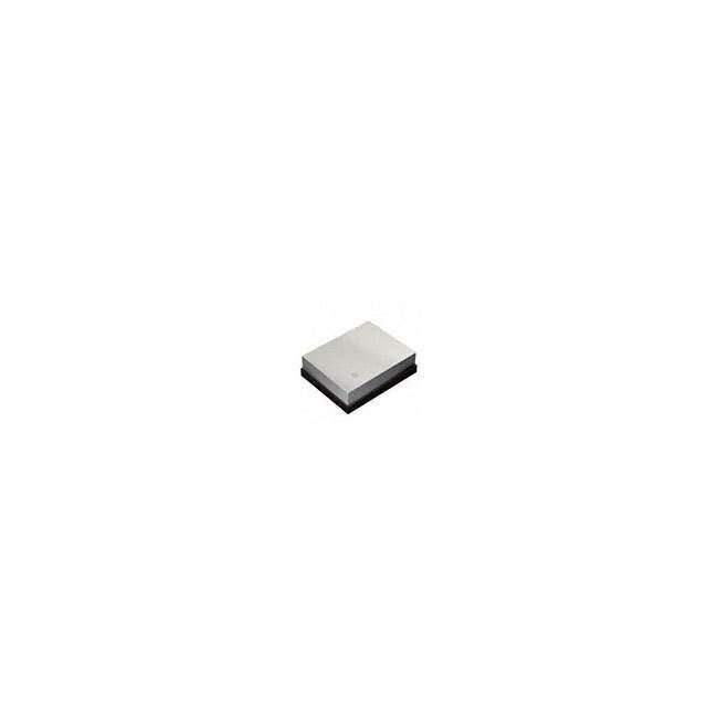
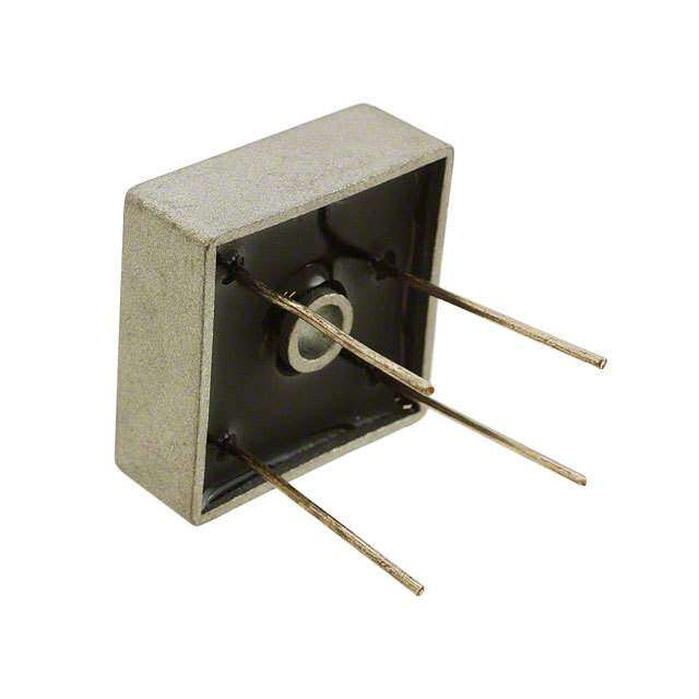
| 产品图片 |
|
| rohs | 符合RoHS无铅 / 符合限制有害物质指令(RoHS)规范要求 |
| 产品系列 | Taiyo Yuden FAR-F6KA-1G9500-D4DG-ZF6 |
| 数据手册 | |
| 产品型号 | FAR-F6KA-1G9500-D4DG-Z |
| 产品 | SAW Filters |
| 产品种类 | 信号调节 |
| 介入损耗 | 1.6 dB |
| 其它名称 | 587-2852-6 |
| 包装 | Digi-Reel® |
| 商标 | Taiyo Yuden |
| 大小/尺寸 | 0.055" 长 x 0.039" 宽(1.40mm x 1.00mm) |
| 安装类型 | 表面贴装 |
| 封装 | Reel |
| 封装/外壳 | 5-SMD,无引线 |
| 封装/箱体 | 1.4 mm x 1 mm x 0.5 mm |
| 工作温度范围 | - 40 C to + 85 C |
| 工厂包装数量 | 3000 |
| 带宽 | 60MHz |
| 应用 | 手机,WCDMA |
| 插入损耗 | 1.6dB |
| 标准包装 | 1 |
| 滤波器类型 | 带通 |
| 端接类型 | SMD/SMT |
| 类型 | SAW Filter |
| 系列 | F6 |
| 频率 | 1.95GHz 中心 |
| 频率范围 | 1000 MHz to 5000 MHz |
| 高度(最大值) | 0.020"(0.50mm) |


- 商务部:美国ITC正式对集成电路等产品启动337调查
- 曝三星4nm工艺存在良率问题 高通将骁龙8 Gen1或转产台积电
- 太阳诱电将投资9.5亿元在常州建新厂生产MLCC 预计2023年完工
- 英特尔发布欧洲新工厂建设计划 深化IDM 2.0 战略
- 台积电先进制程称霸业界 有大客户加持明年业绩稳了
- 达到5530亿美元!SIA预计今年全球半导体销售额将创下新高
- 英特尔拟将自动驾驶子公司Mobileye上市 估值或超500亿美元
- 三星加码芯片和SET,合并消费电子和移动部门,撤换高东真等 CEO
- 三星电子宣布重大人事变动 还合并消费电子和移动部门
- 海关总署:前11个月进口集成电路产品价值2.52万亿元 增长14.8%


PDF Datasheet 数据手册内容提取
Notice for TAIYO YUDEN products Please read this notice before using the TAIYO YUDEN products. REMINDERS ■ Product information in this catalog is as of October 2014. All of the contents specified herein are subject to change without notice due to technical improvements, etc. Therefore, please check for the latest information carefully be- fore practical application or usage of the Products. Please note that TAIYO YUDEN CO., LTD. shall not be responsible for any defects in products or equipment incor- porating such products, which are caused under the conditions other than those specified in this catalog or indi- vidual specification. ■ Please contact TAIYO YUDEN CO., LTD. for further details of product specifications as the individual specification is available. ■ Please conduct validation and verification of products in actual condition of mounting and operating environment before commercial shipment of the equipment. ■ All electronic components or functional modules listed in this catalog are developed, designed and intended for use in general electronics equipment.(for AV, office automation, household, office supply, information service, telecommunications, (such as mobile phone or PC) etc.). Before incorporating the components or devices into any equipment in the field such as transportation,( automotive control, train control, ship control), transportation signal, disaster prevention, medical, public information network (telephone exchange, base station) etc. which may have direct influence to harm or injure a human body, please contact TAIYO YUDEN CO., LTD. for more detail in ad- vance. Do not incorporate the products into any equipment in fields such as aerospace, aviation, nuclear control, subma- rine system, military, etc. where higher safety and reliability are especially required. In addition, even electronic components or functional modules that are used for the general electronic equipment, if the equipment or the electric circuit require high safety or reliability function or performances, a sufficient reliabil- ity evaluation check for safety shall be performed before commercial shipment and moreover, due consideration to install a protective circuit is strongly recommended at customer's design stage. ■ The contents of this catalog are applicable to the products which are purchased from our sales offices or distribu- tors (so called“ TAIYO YUDEN’s official sales channel”). It is only applicable to the products purchased from any of TAIYO YUDEN’ s official sales channel. ■ Please note that TAIYO YUDEN CO., LTD. shall have no responsibility for any controversies or disputes that may occur in connection with a third party's intellectual property rights and other related rights arising from your usage of products in this catalog. TAIYO YUDEN CO., LTD. grants no license for such rights. ■ Caution for export Certain items in this catalog may require specific procedures for export according to“ Foreign Exchange and For- eign Trade Control Law” of Japan,“ U.S. Export Administration Regulations”, and other applicable regulations. Should you have any question or inquiry on this matter, please contact our sales staff. 15
SAW/FBAR DEVICES for MOBILE COMMUNICATIONS REFLOW ■ ORDERING CODE (A)Previous Rule (applied to products registered on March 31, 2010 or before.) F A R − D 6 N F − 1 G 9 6 0 0 − P 1 B Z − Z ❶ ❷ ❸ ❹ ❺ ❻ ❼ ❽ ❾ ❿ ⓫ ⓬ ❶Family ❷Common sign ❹Package type ❼❼FFrreeqquueennccyy ❽Common sign ❿Serial Number − Fixation − Fixation ❸Series ❺Product type ❻Common sign ❾Design ⓫Custom, Status Product Frequency Range − Fixation D5 Duplexer 700-1000MHz ⓬Packing D6 Duplexer 1000-5000MHz J5 Dual Duplexers 700-1000MHz F5 Device 700-1000MHz H F6 Device 1000-5000MHz IG G5 Dual Devices 700-1000MHz H G6 Dual Devices 1000-5000MHz F R (B)New Rule (applied to products registered on April 1, 2010 or later.) E Q U D 6 N F 1 G 9 6 0 P 1 B Z − Z E N C ❶ ❷ ❸ ❹ ❺ ❻ ❼ ❽ Y P R ❶Series ❷Package type ❹Frequency ❺Design ❻Serial Number ❽Packing O Product Frequency Range D D5 Duplexer 700-1000MHz U ❸Product type ❼Custom D6 Duplexer 1000-5000MHz C T J5 Dual Duplexers 700-1000MHz S F5 Device 700-1000MHz F6 Device 1000-5000MHz G5 Dual Devices 700-1000MHz G6 Dual Devices 1000-5000MHz *For further details, please contact to TAIYO YUDEN Co.,Ltd. ■ EXTERNAL DIMENSIONS/STANDARD QUANTITY 2.5×2.0×0.6(8pin) 2.5×2.0×0.6(9pin) 2.5×2.0×0.65 2.0×1.6×0.5 2.5±0.1 0.6max 2.5±0.1 0.6max 2.5±0.1 0.65max 2.0±0.1 0.5max 2.0±0.1 2.0±0.1 2.0±0.1 1.6±0.1 index index index index 4-0.9625 4-0.96252-0.3 4-0.96252-0.3 4-0.775 2-0.325 4-0.7375 C0.15 4-0.7375 0.9×0.375 4-0.7375 0.9×0.375 4-0.575 0.60×0.30 C0.15 C0.15 C0.15 8-0.375 8-0.375 8-0.375 8-0.30 8-0.425 Unit:mm 8-0.425 Unit:mm 8-0.425 Unit:mm 8-0.30 Unit:mm 1.4×1.0×0.5 1.1×0.9×0.5 1.8×1.4×0.5 1.5×1.1×0.5 1.80±0.1 0.5max 1.50±0.1 0.5max 1.40±0.1 0.5max 1.10±0.1 0.5max 1.00±0.1 0.90±0.1 1.40±0.1 1.10±0.1 index index index index 0.50 0.50 0.40 0.40 1.41 1.17 0.47 0.39 0.25 0.20 0.60 0.60 0.39 0.49 0.575 0.25 0.325 0.325 0.5 0.25 0.25 0.25 1.000.25 0.25 0.25 0.780.18 0.18 0.21 0.25 Unit:mm 0.2 Unit:mm 0.24 0.23 Unit:mm 0.180.21 Unit:mm ▶ This catalog contains the typical specification only due to the limitation of space. When you consider the purchase of our products, please check our specification. For details of each product (characteristics graph, reliability information, precautions for use, and so on), see our Web site (http://www.ty-top.com/) . 136 15
■ PART NUMBERS ●Duplexers Package Size Insertion Loss System Part number Isolation( dB) Remarks (mm) (dB) D6PE2G140P3AW 2.0×1.6×0.5 1.5/1.6 59/47 9 Pin, B Type Rx : Bal.100ohm W-CDMA Band 1 D6RB2G140E1AJ 1.8×1.4×0.5 1.7/1.8 57/48 8 Pin, B Type Rx : Bal.100ohm FAR-D6NH-1G9600-M1Z9 2.5×2.0×0.65 2.2/3.1 55/50 9 Pin, B Type FAR-D6NH-1G9600-M1Z6 2.5×2.0×0.65 2.3/2.7 55/53 9 Pin, B Type Low Rx IL FAR-D6NF-1G9600-P1BT 2.5×2.0×0.65 2.5/2.8 54/55 9 Pin, B Type 100ohm, Low Rx IL PCS/W-CDMA Band 2 D6NF1G960P1BR 2.5×2.0×0.65 2.5/3.4 58/53 9 Pin, B Type Rx : Bal.100ohm High GPS Att. & Rx Isol. D6HH1G960BH95 2.5×2.0×0.65 2.3/2.5 56/53 9 Pin, B Type 100ohm D6PE1G960P3BY 2.0×1.6×0.57 2.0/3.1 57/53 9 Pin, B Type Rx : Bal.100ohm W-CDMA Band 4 D6PE2G132P3DWB 2.0×1.6×0.5 1.8/1.8 55/50 9 Pin, B Type Rx : Bal.100ohm FAR-D5NG-881M50-M11Z 2.5×2.0×0.6 1.45/1.8 66/52 9 Pin, B Type FAR-D5PF-881M50-M3E9 2.0×1.6×0.5 1.5/1.8 58/51 9 Pin, B Type FAR-D5NE-881M50-P1A9 2.5×2.0×0.6 1.6/1.8 57/51 9 Pin, B Type Rx : Bal.100ohm CDMA/W-CDMA Band 5 FAR-D5NE-881M50-P1A6Q 2.5×2.0×0.6 1.6/1.7 60/53 9 Pin, B Type 100ohm FAR-D5PE-881M50-P3EZ 2.0×1.6×0.5 1.4/1.7 59/52 9 Pin, B Type Rx : Bal.100ohm FAR-D5PE-881M50-P3EY 2.0×1.6×0.5 1.4/1.7 59/52 9 Pin, A Type Rx : Bal.100ohm D5NL881M5P1HY 3.0×2.5×0.7 1.6/2.6 60/51 SV-LTE FAR-D5NH-942M50-M1Y9 2.5×2.0×0.65 1.8/2.3 58/50 9 Pin, B Type FAR-D5NF-942M50-P1GWQ 2.5×2.0×0.65 1.9/2.3 59/54 9 Pin, B Type 100ohm, GPS High Att. W-CDMA Band 8 D5PF942M5M3G9 2.0×1.6×0.5 1.9/2.2 60/52 9 Pin, B Type D5PE942M5P3GT 2.0×1.6×0.5 1.7/2.2 58/54 9 Pin, B Type Rx : Bal.100ohm D5PE782M0M3P9 2.0×1.6×0.5 1.6/2.0 53/64 9 Pin, B Type LTE Band 13 H D5NL782M0P1JZ 3.0×2.5×0.7 1.9/2.2 66/52 SV-LTE IG FAR-D5NE-740M00-P1C9 2.5×2.0×0.6 1.7/2.0 61/58 9 Pin, B Type Rx : Bal.100ohm LTE Band 17 H D5PE740M0P3NZ 2.0×1.6×0.5 1.9/2.0 63/60 9 Pin, B Type Rx : Bal.100ohm F LTE Band 20 D5NE847M0P1K9 2.5×2.0×0.6 2.1/2.3 52/51 9 Pin, B Type Rx : Bal.100ohm R LTE Band 21 D6PE1G503P3KW 2.0×1.6×0.5 1.6/2.0 55/56 9 Pin, B Type Rx : Bal.100ohm E Q LTE Band 26 D5PE876M5P3UZ 2.0×1.6×0.5 2.2/2.6 60/49 9 Pin, B Type Rx : Bal.100ohm U D5PF773M0M3Y6 2.0×1.6×0.5 1.8/2.3 60/53 Block A 9Pin, B Type E LTE Band 28 D5PF788M0M3Y9 2.0x1.6x0.5 1.8/2.4 60/54 Block B 9Pin, B Type N C D5NF878M0P1ET 2.5×2.0×0.65 1.9/2.5 58/50 9 Pin, B Type Rx : Bal.100ohm CDMA BC0+BC10 Y D5PE878M0P3UT 2.0×1.6×0.5 1.9/2.2 59/51 9 Pin, B Type Rx : Bal.100ohm P R ●CDMA/GSM850/Band 5 O D Package Size Insertion Loss System Part number (mm) (dB) Attenuation( dB) Remarks U FAR-F5KB-836M50-B4ER 1.4×1.0×0.5 1.7 44 100ohm input C T CDMA Tx FAR-F5KB-836M50-B4EG 1.4×1.0×0.5 1.6 42 200ohm input S F5QA836M5M2AR 1.1×0.9×0.5 1.9 45 High Att. CDMA/GSM850 Tx FAR-F5KA-836M50-D4DF 1.4×1.0×0.5 1.9 44 High Att. FAR-F5KB-881M50-B4ED 1.4×1.0×0.5 1.5 61 100ohm output FAR-F5KY-881M50-B4UZ 1.4×1.0×0.5 1.5 61 100ohm, High Att. CDMA/W-CDMA Band 5 Rx FAR-F5KB-881M50-B4EJ 1.4×1.0×0.5 1.4 64 200ohm output FAR-F5QB-881M50-P2BG 1.1×0.9×0.5 1.5 60 100ohm output F5QG881M5P2KG 1.1×0.9×0.5 1.5 56 100ohm, High Att., Low Loss FAR-F5KA-881M50-D4DB 1.4×1.0×0.5 1.7 56 High Att. GSM850/CDMA Rx FAR-F5QA-881M50-M2AF 1.1×0.9×0.5 1.6 46 - FAR-F5KB-881M50-B4EA 1.4×1.0×0.5 1.7 53 150ohm output GSM850 Rx FAR-F5QB-881M50-P2BA 1.1×0.9×0.5 1.3 63 150ohm output ●CDMA2000 BC0+BC10 Package Size Insertion Loss System Part number Attenuation( dB) Remarks (mm) (dB) F5KA833M0D4DU 1.4×1.0×0.5 2.3 43 High Att. CDMA2000 BC0+10 Tx F5KA833M0D4MG 1.4×1.0×0.5 1.4 20 Low IL CDMA2000 BC0+10 Rx F5KY878M0B4ND 1.4×1.0×0.5 2.1 53 100ohm output ●GSM/EGSM/Band 8 Package Size Insertion Loss System Part number Attenuation( dB) Remarks (mm) (dB) FAR-F5KA-897M50-D4DC 1.4×1.0×0.5 2.2 16 High Att. EGSM Tx FAR-F5KA-897M50-D4VW 1.4×1.0×0.5 2.6 38 High Att. F5QA897M5M2AC 1.1×0.9×0.5 2.3 18 − FAR-F5KA-942M50-D4DD 1.4×1.0×0.5 2.0 34 High Att. FAR-F5KB-942M50-B4EB 1.4×1.0×0.5 1.6 26 150ohm output EGSM Rx FAR-F5KB-942M50-B4ES 1.4×1.0×0.5 2.4 29 100ohm output FAR-F5QB-942M50-P2BB 1.1×0.9×0.5 1.6 28 150ohm output F5KA942M5D4MYB 1.4×1.0×0.5 1.9 53 High Att. W-CDMA/LTE Band 8 FAR-F5KY-942M50-B4UW 1.4×1.0×0.5 2.0 57 100ohm, High Att. F5QG942M5P2KB 1.1×0.9×0.5 2.2 56 100ohm, High Att. ▶ This catalog contains the typical specification only due to the limitation of space. When you consider the purchase of our products, please check our specification. For details of each product (characteristics graph, reliability information, precautions for use, and so on), see our Web site (http://www.ty-top.com/) . 15 137
■ PART NUMBERS ●DCS/Band 3 Package Size Insertion Loss System Part number Attenuation( dB) Remarks (mm) (dB) FAR-F6KA-1G7475-D4CY 1.4×1.0×0.5 2.5 30 DCS Tx F6QA1G747M2QS 1.1×0.9×0.5 2.1 22 FAR-F6KA-1G8425-D4CK 1.4×1.0×0.5 2.1 20 FAR-F6KB-1G8425-B4GA 1.4×1.0×0.5 1.5 14 150ohm output DCS Rx F6QB1G842P2BM 1.1×0.9×0.5 1.8 15 100ohm F6QB1G842P2BF 1.1×0.9×0.5 1.6 17 150ohm W-CDMA/LTE Band 3 F6KY1G842B4UM 1.4×1.0×0.5 3.0 50 100ohm, High Att. ●PCS/GSM1900/Band 2 Package Size Insertion Loss System Part number Attenuation( dB) Remarks (mm) (dB) FAR-F6KA-1G8800-L4AF 1.4×1.0×0.5 2.4 35 High Att. US-PCS Tx FAR-F6KB-1G8800-B4GS 1.4×1.0×0.5 2.3 28 100ohm input F6QA1G880M2AQ 1.1×0.9×0.5 1.7 20 FAR-F6KA-1G9600-D4MT 1.4×1.0×0.5 3.4 43 High Att. FAR-F6KB-1G9600-B4GP 1.4×1.0×0.5 2.1 23 100ohm output US-PCS Rx FAR-F6KY-1G9600-B4UU 1.4×1.0×0.5 2.9 49 100ohm, High Att. F6KY1G960B4NF 1.4×1.0×0.5 2.8 50 100ohm output F6QG1G960P2KT 1.1×0.9×0.5 2.8 44 100ohm output GSM1900/US-PCS Rx FAR-F6KA-1G9600-D4CR 1.4×1.0×0.5 2.0 18 FAR-F6KB-1G9600-B4GB 1.4×1.0×0.5 1.6 18 150ohm output H GSM1900 Rx F6QB1G960P2BK 1.1×0.9×0.5 1.5 15 150ohm output IG H ●GSM Dual F R System Part number Package Size Insertion Loss Attenuation( dB) Remarks E (mm) (dB) Q GSM850+EGSM Rx FAR-G5QC-942M50-N2FB 1.5×1.1×0.5 1.5/1.8 50/29 GSM850 150ohm output EGSM 150ohm output U GSM850+EGSM Rx FAR-G5KT-942M50-Y4RW 1.8×1.4×0.5 1.9/2.2 50/25 GSM850 150ohm output EGSM 150ohm output E (Common Input) N GSM850+EGSM Rx FAR-G5KW-942M50-Y4YD 1.8×1.4×0.5 2.5/1.8 32/38 EGSM 150ohm output GSM850 150ohm output C (Common Output) Y FAR-G5KC-942M50-Y4YW 1.8×1.4×0.5 1.8/1.4 31/54 EGSM 150ohm output GSM850 150ohm output P EGSM+GSM850 Rx FAR-G5QC-942M50-N2CD 1.5×1.1×0.5 1.7/1.4 29/51 EGSM 150ohm output GSM850 150ohm output R EGSM+GSM850 Rx FAR-G5KT-942M50-Y4RZ 1.8×1.4×0.5 2.2/1.9 25/52 EGSM 150ohm output GSM850 150ohm output O (Common Input) FAR-G5QD-942M50-N2DB 1.5×1.1×0.5 2.5/2.0 25/55 EGSM 150ohm output GSM850 150ohm output D FAR-G6QC-1G9600-N2FA 1.5×1.1×0.5 1.9/1.7 17/13 DCS 150ohm output GSM1900 150ohm output U DCS+GSM1900 Rx G6QJ1G960M2MB 1.5×1.1×0.5 1.9/1.9 19/19 Rx Dual Unbal C DCS+GSM1900 Rx T (Common Input) FAR-G6KT-1G9600-Y4RU 1.8×1.4×0.5 1.8/2.0 18/13 DCS 150ohm output GSM1900 150ohm output S DCS+GSM1900 Rx G6QD1G960N2DY 1.5×1.1×0.5 1.8/1.9 18/14 1 IN 4 OUT 150ohm output (Common Input) FAR-G6KC-1G9600-Y4YY 1.8×1.4×0.5 1.9/1.8 14/16 GSM1900 150ohm output DCS 150ohm output GSM1900+DCS Rx G6QC1G960N2CH 1.5×1.1×0.5 1.6/1.6 13/15 GSM1900 150ohm output DCS 150ohm output GSM1900+DCS Rx FAR-G6KT-1G9600-Y4RY 1.8×1.4×0.5 1.9/1.8 13/18 GSM1900 150ohm output DCS 150ohm output (Common Input) FAR-G6KW-1G9600-Y4YC 1.8×1.4×0.5 2.2/3.1 13/15 170ohm output for IMC GSM1900+DCS Rx G6QE1G960N2EC 1.5×1.1×0.5 2.5/2.5 18/13 GSM1900 150ohm output DCS 150ohm output (Common Output) G6QE1G960N2EE 1.5×1.1×0.5 2.2/2.2 31/14 GSM1900/DCS 150ohm output Low Loss GSM1900+850 Rx G6QF1G960N2GA 1.5×1.1×0.5 1.6/1.4 14/54 GSM1900 150ohm output GSM850 150ohm output ●GPS Package Size Insertion Loss System Part number Attenuation( dB) Remarks (mm) (dB) FAR-F6KA-1G5754-L4AJ 1.4×1.0×0.5 0.9 − Low loss, High Att. F6QA1G575H2JF 1.1×0.9×0.5 0.96 − Low loss, High Att. GPS FAR-F6KB-1G5754-B4GE 1.4×1.0×0.5 1.1 − 100ohm, Low loss FAR-F6KB-1G5754-B4GU 1.4×1.0×0.5 1.2 − 100ohm, High Att. FAR-F6KA-1G5859-D4MS 1.4×1.0×0.5 1.0/1.2 − − F6QA1G585M2AT 1.1×0.9×0.5 1.1/1.4 − − GPS/GNSS FAR-F6KB-1G5859-B4HR 1.4×1.0×0.5 1.1/1.4 − 100ohm output F6QB1G585P2BQ 1.1×0.9×0.5 1.5/1.7 − 100ohm output GPS+GLONASS+Galileo F6KA1G581D4JR 1.4×1.0×0.5 1.6 − +Compass F6QA1G581M2QZ 1.1×0.9×0.5 1.1/1.4 − ▶ This catalog contains the typical specification only due to the limitation of space. When you consider the purchase of our products, please check our specification. For details of each product (characteristics graph, reliability information, precautions for use, and so on), see our Web site (http://www.ty-top.com/) . 138 15
■ PART NUMBERS ●W-CDMA Package Size Insertion Loss System Part number Attenuation( dB) Remarks (mm) (dB) FAR-F6KA-1G9500-D4DG 1.4×1.0×0.5 1.6 38 Low loss, High Att. W-CDMA Band 1 Tx FAR-F6KB-1G9500-B4GJ 1.4×1.0×0.5 2.1 34 100ohm output F6QA1G950M2AA 1.1×0.9×0.5 1.8 38 Low loss, High Att. FAR-F6KA-2G1400-D4CG 1.4×1.0×0.5 1.9 39 FAR-F6KB-2G1400-B4GC 1.4×1.0×0.5 1.7 39 100ohm output W-CDMA Band 1 Rx FAR-F6KA-2G1400-D4DW 1.4×1.0×0.5 1.9 48 High Att. FAR-F6KY-2G1400-B4UY 1.4×1.0×0.5 1.8 64 100ohm, High Att. F6QG2G140P2KA 1.1×0.9×0.5 1.7 55 100ohm, High Att. W-CDMA Band 1+2 Rx G6QL2G140M2PA 1.5×1.1×0.5 1.9/3.0 48/41 W-CDMA Band 2+1 Rx G6QH2G140N2LP 1.5×1.1×0.5 3.2/2.3 53/54 2 (1.9G)100ohm out 1 (2G)100ohm out W-CDMA Band 4 Tx FAR-F6KA-1G7400-D4DE 1.4×1.0×0.5 1.5 44 W-CDMA Band 5+8 Rx G5QH942M5N2LN 1.5×1.1×0.5 1.6/20 56/50 100ohm output W-CDMA Band 8+5 Rx G5QT942M5N2VA 1.5×1.1×0.5 2.3/2.0 48/48 100ohm output (Common Output) W-CDMA Band 7 Tx F6KA2G535L4AM 1.4×1.0×0.5 1.6 30 FAR-F6KY-2G6550-B4UN 1.4×1.0×0.5 2.8 54 100ohm. High Att. W-CDMA/LTE Band 7 Rx F6QG2G655P2KE 1.1×0.9×0.5 2.5 52 100ohm. High Att. W-CDMA Band 9 Tx FAR-F6KA-1G7675-D4CT 1.4×1.0×0.5 1.8 31 Unbal. W-CDMA Band 9 Rx FAR-F6KB-1G8625-B4GT 1.4×1.0×0.5 2.1 40 100ohm output LTE Band 12 Tx F5KA707M5D4JW 1.4×1.0×0.5 1.6 23 Unbal. LTE Band 12 Rx F5KY737M0B4NN 1.4×1.0×0.5 1.4 57 100ohm output FAR-F5KA-782M00-D4VP 1.4×1.0×0.5 1.5 55 H LTE Band 13 Tx F5QA782M0M2AZ 1.1×0.9×0.5 1.5 56 Unbal. IG LTE Band 13 Rx FAR-F5KY-751M00-B4UQ 1.4×1.0×0.5 1.6 50 100ohm output H F5QA751M0M2QM 1.1×0.9×0.5 1.9 50 Unbal. F LTE Band 17 Tx FAR-F5KA-710M00-D4VQ 1.4×1.0×0.5 1.2 32 R F5QA710M0M2AY 1.1×0.9×0.5 1.3 33 Unbal. E FAR-F5KY-740M00-B4UR 1.4×1.0×0.5 1.4 60 100ohm output Q LTE Band 17 Rx F5QG740M0P2KH 1.1×0.9×0.5 1.4 65 100ohm output U LTE Band 18 Tx F5KA822M5D4VR 1.1×0.9×0.5 1.6 40 Unbal. E N LTE Band 18+5 (BC0) Tx F5KA832M0D4JS 1.4×1.0×0.5 1.5 19 Unbal. C LTE Band 20 Tx F5KA847M0D4ML 1.4×1.0×0.5 1.7 52 Y F5KY806M0B4NE 1.4×1.0×0.5 2.5 45 100ohm output LTE Band 20 Rx P F5QA806M0M2QE 1.1×0.9×0.5 2.7 41 Unbal. R F6KY1G503B4NS 1.4×1.0×0.5 1.4 47 100ohm output Low loss O LTE Band 21 Rx F6QA1G503M2QF 1.1×0.9×0.5 2.0 52 Unbal. D LTE Band 25 Tx F6QA1G882M2AS 1.1×0.9×0.5 1.8 23 Unbal. U LTE Band 26 Rx F5QG876M5P2KQ 1.1×0.9×0.5 2.2 59 100ohm output C F5QA773M0M2QC 1.1×0.9×0.5 2.1 52 Block A T LTE Band 28 Rx S F5QA788M0M2QB 1.1×0.9×0.5 2.0 52 Block B LTE Band 29 Rx F5BA722M5M6UW 1.1×0.9×0.5 1.6 38 Unbal. TD LTE Bnad 38 Rx F6KB2G595B4HS 1.4×1.0×0.5 2.6 − 150ohm output TD LTE Band 38+40 G6QE2G595N2EJ 1.5×1.1×0.5 2.9/2.8 − Balanced 100ohm (Common output) F6KB2G350B4HT 1.4×1.0×0.5 2.7 − 150ohm output TD LTE Band 40 Rx F6KB2G350B4HTB 1.4×1.0×0.5 2.5 − Balanced 100ohm ●Other Package Size Insertion Loss System Part number Attenuation( dB) Remarks (mm) (dB) ISM900 (B.W.26MHz) FAR-F5QA-915M00-M2AK 1.1×0.9×0.5 1.8 − TD-SCDMA/TD-LTE Band 34 FAR-F6KA-2G0175-D4DR 1.4×1.0×0.5 1.8 − High Att TD-SCDMA/TD-LTE Band 39 FAR-F6KA-1G9000-D4DS 1.4×1.0×0.5 1.6 − G6QJ2G017M2MD 1.5×1.1×0.5 1.3/1.4 − 2 IN/2 OUT TD-SCDMA Band 34+39 G6QJ2G017M2RD 1.5×1.1×0.5 1.6/2.0 − 1 IN/2 OUT TD-SCDMA Band 39+34 G6QD2G017N2DU 1.5×1.1×0.5 1.7/2.0 − Balanced 100ohm (Common input) TD-SCDMA Band 34+39 G6QD2G017N2DC 1.5×1.1×0.5 2.2/1.8 − Balanced 200ohm (Common input) FAR-F6KA-2G4418-D4CU 1.4×1.0×0.5 2.6 − +10dBm FAR-F6KA-2G4418-A4VA 1.4×1.0×0.5 3.0 − +23dBm Wireless LAN FAR-F6KA-2G4500-A4VD 1.4×1.0×0.5 1.9 − Low IL,+19dBm F6KA2G436A4VE 1.4×1.0×0.5 2.5 − BW=72MHz,+24dBm F6KA2G466A4VJ 1.4×1.0×0.5 2.8 − BW=68MHz,+24dBm ▶ This catalog contains the typical specification only due to the limitation of space. When you consider the purchase of our products, please check our specification. For details of each product (characteristics graph, reliability information, precautions for use, and so on), see our Web site (http://www.ty-top.com/) . 15 139
SAW/FBAR DEVICES (FILTER / DUPLEXERS) ■PACKAGING ①Minimum Quantity Type Size(mm) Code & Quantity(Pieces) 3.0×2.5 Z 3000 U 10000 Duplexer 2.5×2.0 Z 3000 U 10000 2.0×1.6 Z 3000 Y 15000 2.0×1.6 Z 3000 Y 15000 Single Filter 1.4×1.0 Z 3000 Y 15000 1.1×0.9 J 5000 Y 15000 2.0×1.6 Z 3000 Y 15000 Dual Filter 1.8×1.4 Z 3000 Y 15000 1.5×1.1 J 5000 Y 15000 ②Tape material ●Taping dimensions Type Size(mm) a b c d e f 3.0×2.5 3.4±0.1 2.85±0.1 1.05±0.05 1.55±0.05 1.0±0.1 0.25±0.05 Duplexer 2.5×2.0 2.8±0.1 2.3±0.1 1.5+0.1/-0 1.5+0.1/-0 1.0+0.1/-0.0 0.25±0.05 2.0×1.6 2.4±0.1 2.0±0.1 1.05±0.05 1.5+0.1/-0 0.90-0.05 0.25±0.05 2.0×1.6 2.4±0.1 2.0±0.1 1.05±0.05 1.5+0.1/-0 0.90-0.05 0.25±0.05 Single Filter 1.4×1.0 1.7±0.1 1.3±0.1 0.5±0.05 1.5+0.1/-0 0.63±0.05 0.20±0.05 1.1×0.9 1.3±0.1 1.1±0.1 0.5±0.05 1.55±0.05 0.63±0.05 0.20±0.05 2.0×1.6 2.4±0.1 2.0 1.05±0.05 1.5+0.1/-0 0.90-0.05 0.25±0.05 Dual Filter 1.8×1.4 2.2±0.1 1.8 0.5±0.05 1.55±0.05 0.8±0.1 0.30±0.05 1.5×1.1 1.8±0.1 1.4 0.5±0.05 1.5+0.1/-0 0.7±0.1 0.25±0.05 Unit:mm ●Material of Tape(Conductive) Tape : Polystyrene Top cover tape : Polyethylene terephthalate(PET)and Polyethylene ③Top Tape Strength The top tape requires a peel-off force of 0.1 to 1.0N in the direction of the arrow as illustrated below. ▶ This catalog contains the typical specification only due to the limitation of space. When you consider the purchase of our products, please check our specification. For details of each product (characteristics graph, reliability information, precautions for use, and so on), see our Web site (http://www.ty-top.com/) . sawfilter_pack_e-E02R01
④Reel size ●Material of Reel Material : Polystyrene+Carbon Characteristics : Conform to EIAJ-ET-7200A Color : Black Surface resistance(reference value) :109Ω/sq Max. Code Quantity A B C W1 W2 Z 3,000 pcs φ180.0 +0.0/-1.5 φ66.0 ±0.5 φ13.0 ±0.2 9.0 +1.0/-0.0 11.4 ±1.0 J 5,000 pcs φ180.0 +0.0/-1.5 φ66.0 ±0.5 φ13.0 ±0.2 9.0 +1.0/-0.0 11.4 ±1.0 U 10,000 pcs φ330.0 ±2.0 φ100.0 ±1.0 φ13.0 ±0.2 9.4 ±1.0 13.4 ±1.0 Y 15,000 pcs φ330.0 ±2.0 φ100.0 ±1.0 φ13.0 ±0.2 9.4 ±1.0 13.4 ±1.0 Unit:mm ⑤Reel label and Reel C-Label sticking and Winding method ●Surface ▶ This catalog contains the typical specification only due to the limitation of space. When you consider the purchase of our products, please check our specification. For details of each product (characteristics graph, reliability information, precautions for use, and so on), see our Web site (http://www.ty-top.com/) . sawfilter_pack_e-E02R01
Filter ■RELIABILITY DATA 1. Terminal stregth Specified Value No damage to be found. Bending Test. according to IEC60068-2-21(JISC60068-2-21) Test Methods and Remarks 2. Mechanical shock Specified Value After testing, meet the specified characteristics at a room temperature. Test Methods and Apply 14700m/s2 for 0.5ms 5 times for each of 6 directions. Remarks according to IEC68-2-27(JISC60068-2-27). 3. Vibration Specified Value After testing, meet the specified characteristics at a room temperature. Test Methods and With 1.5 mm of whole amplitude at 10 to 55 Hz of frequency, and 98m/s2 of acceleration at 55 to 500Hz, apply a Remarks vibration for 2 hours for each of 3 directions, period is 15 minutes(10 to 500 to 10Hz) 4. Drop 1 Specified Value After testing, meet the specified characteristics at a room temperature. Test Methods and Drop 3 times onto concrete floor from the height of 1.0m. Remarks 5. Drop 2 Specified Value After testing, meet the specified characteristics at a room temperature. Test Methods and Drop with 150g weight 3 times in each 6 direction onto concrete floor from the height of 1.8m. Remarks 6. Temperature cycling Specified Value After testing, meet the specified characteristics at a room temperature. Test Methods and Temp. range -40 to +100℃. 500cycle. Remarks 7. Static humidity Specified Value After testing, meet the specified characteristics at a room temperature. Test Methods and +85℃, 90% to 95%RH, apply DC5V, 1000hours. Remarks 8. High temperature storage life Specified Value After testing, meet the specified characteristics at a room temperature. Test Methods and +100℃, 1000hours. Remarks 9. Low temperature storage life Specified Value After testing, meet the specified characteristics at a room temperature. Test Methods and -40℃, 1000hours. Remarks ▶ This catalog contains the typical specification only due to the limitation of space. When you consider the purchase of our products, please check our specification. For details of each product (characteristics graph, reliability information, precautions for use, and so on), see our Web site (http://www.ty-top.com/) . sawfilter_reli_e-E02R01
10. Solderbility 1 More than 90% of area of terminals to be covered with the solder. Specified Value A change of the remarkable appearance do not have it. Test Methods and Lead-free Solder paste, Reflow;Peak temperature 245℃ Remarks 11. Solderbility 2 More than 90% of area of terminals to be covered with the solder. Specified Value A change of the remarkable appearance do not have it. Test Methods and Sn-Pb Solder paste, Reflow;Peak temperature 235℃ Remarks 12. Solder heat resistance After testing, meet the specified characteristics at a room temperature. Specified Value A change of the remarkable appearance do not have it. ◆Recommended temperature profile of reflow soldering Figure shows recommended temperature profile of reflow soldering in the case of lead-free solder alloy Sn3.0Ag0.5Cu. Suitable condition for solder heating is differed depending on composition and manufacturing method. Please contact to solder manufacturer for the details. Test Methods and Remarks ▶ This catalog contains the typical specification only due to the limitation of space. When you consider the purchase of our products, please check our specification. For details of each product (characteristics graph, reliability information, precautions for use, and so on), see our Web site (http://www.ty-top.com/) . sawfilter_reli_e-E02R01
Duplexer ■RELIABILITY DATA 1. Terminal stregth Specified Value No damage to be found. Bend width 4mm, hold for 5±1 sec. according to IEC60068-2-21(JISC60068-2-21) Test Methods and Remarks 2. Mechanical shock Specified Value After testing, meet the specified characteristics at a room temperature. Test Methods and Apply 14700m/s2 for 0.5ms 5 times for each of 6 directions. Remarks according to IEC68-2-27(JISC60068-2-27). 3. Vibration Specified Value After testing, meet the specified characteristics at a room temperature. Test Methods and With 1.5 mm of whole amplitude at 10 to 55 Hz of frequency, and 98m/s2 of acceleration at 55 to 500Hz, apply a Remarks vibration for 2 hours for each of 3 directions, period is 15 minutes(10 to 500 to 10Hz) 4. Drop 1 Specified Value After testing, meet the specified characteristics at a room temperature. Test Methods and Drop 3 times onto concrete floor from the height of 1.0m. Remarks 5. Drop 2 Specified Value After testing, meet the specified characteristics at a room temperature. Test Methods and Drop with 150g weight 3 times in each 6 direction onto concrete floor from the height of 1.8m. Remarks 6. Temperature cycling Specified Value After testing, meet the specified characteristics at a room temperature. Test Methods and Temp. range -40 to +100℃. 500cycle. Remarks 7. Static humidity Specified Value After testing, meet the specified characteristics at a room temperature. Test Methods and +85℃, 90% to 95%RH, apply DC5V, 1000hours. Remarks 8. High temperature storage life Specified Value After testing, meet the specified characteristics at a room temperature. Test Methods and +100℃, 1000hours. Remarks 9. Low temperature storage life Specified Value After testing, meet the specified characteristics at a room temperature. Test Methods and -40℃, 1000hours. Remarks ▶ This catalog contains the typical specification only due to the limitation of space. When you consider the purchase of our products, please check our specification. For details of each product (characteristics graph, reliability information, precautions for use, and so on), see our Web site (http://www.ty-top.com/) . sawfilter_reli_e-E02R01
10. High Temperature Bias Specified Value After testing, meet the specified characteristics at a room temperature. Test Methods and +50℃, +29dBm, 50000hours. Remarks 11. Solderbility 1 More than 90% of area of terminals to be covered with the solder. Specified Value A change of the remarkable appearance do not have it. Test Methods and Lead-free Solder paste, Reflow;Peak temperature 245℃ Remarks 12. Solderbility 2 More than 90% of area of terminals to be covered with the solder. Specified Value A change of the remarkable appearance do not have it. Test Methods and Sn-Pb Solder paste, Reflow;Peak temperature 235℃ Remarks 13. Solder heat resistance After testing, meet the specified characteristics at a room temperature. Specified Value A change of the remarkable appearance do not have it. ◆Recommended temperature profile of reflow soldering Figure shows recommended temperature profile of reflow soldering in the case of lead-free solder alloy Sn3.0Ag0.5Cu. Suitable condition for solder heating is differed depending on composition and manufacturing method. Please contact to solder manufacturer for the details. Test Methods and Remarks ▶ This catalog contains the typical specification only due to the limitation of space. When you consider the purchase of our products, please check our specification. For details of each product (characteristics graph, reliability information, precautions for use, and so on), see our Web site (http://www.ty-top.com/) . sawfilter_reli_e-E02R01