ICGOO在线商城 > 集成电路(IC) > PMIC - 栅极驱动器 > FAN73611MX
 Datasheet下载
- 型号: FAN73611MX
- 制造商: Fairchild Semiconductor
- 库位|库存: xxxx|xxxx
- 要求:
| 数量阶梯 | 香港交货 | 国内含税 |
| +xxxx | $xxxx | ¥xxxx |
查看当月历史价格
查看今年历史价格
FAN73611MX产品简介:
ICGOO电子元器件商城为您提供FAN73611MX由Fairchild Semiconductor设计生产,在icgoo商城现货销售,并且可以通过原厂、代理商等渠道进行代购。 FAN73611MX价格参考。Fairchild SemiconductorFAN73611MX封装/规格:PMIC - 栅极驱动器, High-Side Gate Driver IC Non-Inverting 8-SOP。您可以下载FAN73611MX参考资料、Datasheet数据手册功能说明书,资料中有FAN73611MX 详细功能的应用电路图电压和使用方法及教程。
FAN73611MX是由ON Semiconductor(安森美半导体)制造的一款PMIC(电源管理集成电路),具体分类为栅极驱动器。该器件主要用于驱动功率MOSFET或IGBT的栅极,广泛应用于各种电力电子设备中。

 应用场景:

1. 开关电源(SMPS):
   FAN73611MX常用于开关电源的设计中,特别是在高效率、高性能的AC-DC和DC-DC转换器中。它能够提供快速的开关速度和低延迟,确保高效的功率转换。适用于笔记本电脑适配器、手机充电器、LED驱动电源等消费电子产品。

2. 电机驱动:
   在电机驱动应用中,FAN73611MX可以驱动逆变器中的功率MOSFET或IGBT,实现对电机的精确控制。其高电流驱动能力使得它可以处理大功率电机,如电动工具、家用电器中的电机驱动系统。

3. 太阳能逆变器:
   太阳能光伏发电系统中的逆变器需要高效的功率转换和可靠的栅极驱动。FAN73611MX凭借其高可靠性和低功耗特性,成为太阳能逆变器的理想选择,能够提高系统的整体效率和稳定性。

4. 不间断电源(UPS):
   UPS系统需要在市电中断时迅速切换到电池供电模式,确保负载的连续供电。FAN73611MX可以驱动UPS中的功率开关器件,确保快速响应和稳定的输出电压。

5. 工业自动化:
   在工业自动化领域,FAN73611MX可用于驱动PLC(可编程逻辑控制器)、伺服驱动器和其他工业控制设备中的功率器件。其高可靠性有助于提高整个系统的稳定性和耐用性。

6. 汽车电子:
   随着电动汽车和混合动力汽车的发展,FAN73611MX在车载充电器、DC-DC转换器以及电动助力转向系统(EPS)等应用中也得到了广泛应用。其抗干扰能力强,能够在恶劣的汽车环境中稳定工作。

 总结:
FAN73611MX凭借其高效、可靠的性能,在多个领域的电力电子设备中发挥着重要作用。无论是消费电子、工业自动化还是新能源领域,它都能为系统提供强大的栅极驱动支持,确保功率器件的高效运行和系统的稳定性能。
| 参数 | 数值 |
| 产品目录 | 集成电路 (IC)半导体 |
| 描述 | IC GATE DVR HIGH SIDE 1CH 8-SOIC门驱动器 HI-SPEED GATE DRIVER |
| 产品分类 | PMIC - MOSFET,电桥驱动器 - 外部开关集成电路 - IC |
| 品牌 | Fairchild Semiconductor |
| 产品手册 | |
| 产品图片 |
|
| rohs | 符合RoHS无铅 / 符合限制有害物质指令(RoHS)规范要求 |
| 产品系列 | 电源管理 IC,门驱动器,Fairchild Semiconductor FAN73611MX- |
| 数据手册 | |
| 产品型号 | FAN73611MX |
| 上升时间 | 70 ns |
| 下降时间 | 30 ns |
| 产品 | MOSFET Gate Drivers |
| 产品种类 | 门驱动器 |
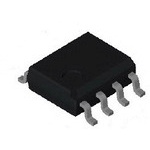
| 供应商器件封装 | 8-SOP |
| 其它名称 | FAN73611MXCT |
| 包装 | 剪切带 (CT) |
| 单位重量 | 143 mg |
| 商标 | Fairchild Semiconductor |
| 安装类型 | 表面贴装 |
| 安装风格 | SMD/SMT |
| 封装 | Reel |
| 封装/外壳 | 8-SOIC(0.154",3.90mm 宽) |
| 封装/箱体 | SOP-8 |
| 工作温度 | -40°C ~ 125°C |
| 工厂包装数量 | 3000 |
| 延迟时间 | 120ns |
| 最大功率耗散 | 0.625 W |
| 最大工作温度 | + 125 C |
| 最小工作温度 | - 40 C |
| 标准包装 | 1 |
| 激励器数量 | 1 |
| 电压-电源 | 10 V ~ 20 V |
| 电流-峰值 | 250mA |
| 电源电压-最大 | 20 V |
| 电源电压-最小 | 10 V |
| 电源电流 | 30 uA |
| 类型 | High Side Driver |
| 系列 | FAN7361 |
| 输入类型 | 非反相 |
| 输出数 | 1 |
| 输出电流 | 0.5 A |
| 配置 | 高端 |
| 配置数 | 1 |
| 高压侧电压-最大值(自举) | 600V |


PDF Datasheet 数据手册内容提取
Is Now Part of To learn more about ON Semiconductor, please visit our website at www.onsemi.com Please note: As part of the Fairchild Semiconductor integration, some of the Fairchild orderable part numbers will need to change in order to meet ON Semiconductor’s system requirements. Since the ON Semiconductor product management systems do not have the ability to manage part nomenclature that utilizes an underscore (_), the underscore (_) in the Fairchild part numbers will be changed to a dash (-). This document may contain device numbers with an underscore (_). Please check the ON Semiconductor website to verify the updated device numbers. The most current and up-to-date ordering information can be found at www.onsemi.com. Please email any questions regarding the system integration to Fairchild_questions@onsemi.com. ON Semiconductor and the ON Semiconductor logo are trademarks of Semiconductor Components Industries, LLC dba ON Semiconductor or its subsidiaries in the United States and/or other countries. ON Semiconductor owns the rights to a number of patents, trademarks, copyrights, trade secrets, and other intellectual property. A listing of ON Semiconductor’s product/patent coverage may be accessed at www.onsemi.com/site/pdf/Patent-Marking.pdf. ON Semiconductor reserves the right to make changes without further notice to any products herein. ON Semiconductor makes no warranty, representation or guarantee regarding the suitability of its products for any particular purpose, nor does ON Semiconductor assume any liability arising out of the application or use of any product or circuit, and specifically disclaims any and all liability, including without limitation special, consequential or incidental damages. Buyer is responsible for its products and applications using ON Semiconductor products, including compliance with all laws, regulations and safety requirements or standards, regardless of any support or applications information provided by ON Semiconductor. “Typical” parameters which may be provided in ON Semiconductor data sheets and/or specifications can and do vary in different applications and actual performance may vary over time. All operating parameters, including “Typicals” must be validated for each customer application by customer’s technical experts. ON Semiconductor does not convey any license under its patent rights nor the rights of others. ON Semiconductor products are not designed, intended, or authorized for use as a critical component in life support systems or any FDA Class 3 medical devices or medical devices with a same or similar classification in a foreign jurisdiction or any devices intended for implantation in the human body. Should Buyer purchase or use ON Semiconductor products for any such unintended or unauthorized application, Buyer shall indemnify and hold ON Semiconductor and its officers, employees, subsidiaries, affiliates, and distributors harmless against all claims, costs, damages, and expenses, and reasonable attorney fees arising out of, directly or indirectly, any claim of personal injury or death associated with such unintended or unauthorized use, even if such claim alleges that ON Semiconductor was negligent regarding the design or manufacture of the part. ON Semiconductor is an Equal Opportunity/Affirmative Action Employer. This literature is subject to all applicable copyright laws and is not for resale in any manner.
F A N 7 3 September 2015 6 1 1 — S i n FAN73611 g l e - Single-Channel High-Side Gate Drive IC C h a n n Features The FAN73611 is a monolithic high-side gate drive IC e Floating Channel for Bootstrap Operation to +600V that can drive MOSFETs and IGBTs operating up to l H +600V. Fairchild’s high-voltage process and common- i 250mA/500mA Sourcing/Sinking Current Driving g mode noise canceling techniques provide stable opera- h Capability tion of the high-side driver under high dv/dt noise circum- - S Common-Mode dv/dt Noise-Canceling Circuit stances. An advanced level-shift circuit offers high-side i d 3.3V and 5V Input Logic Compatible gate driver operation up to VS=-9.8V (typical) for e Output In Phase with Input Signal VBS=15V. The UVLO circuits prevents malfunction when G V or V is lower than the specified threshold voltage. a Under-Voltage Lockout for VDD and VBS DD BS te The output drivers typically source/sink 250mA/500mA; 8-Lead Small Outline Package (SOP) D respectively, which is suitable for Plasma Display Panel r (PDP) application, motor drive inverter, and switching iv mode power supply applications. e I C Applications 8-SOP Electronic Ballast Switching-Mode Power Supply (SMPS) Related Application Notes AN-6076 — Design and Applicaiton Guide of Boostrap Circuit for High-Voltage Gate-Drive IC AN-9052 — Design Guide for Selection of Bootstrap Components AN-8102 — Recommendations to Avoid Short Pulse Width Issues in HVIC Gate Driver Applications Description Ordering Information Part Number Package Operating Temperature Packing Method Description FAN73611MX(1) 8 SOP -40°C ~ 125°C Tape & Reel Lighting Application Note: 1. This device passed wave soldering test by JESD22A-111. © 2010 Fairchild Semiconductor Corporation www.fairchildsemi.com FAN73611 • Rev. 1.3
F A Typical Application Diagrams N 7 3 6 1 1 — 15V VIN S i RBOOT DBOOT ng l e FAN73611 - C h 1 VDD VB 8 a n R1 n PWM 2 IN HO 7 e l CBOOT R2 L1 H C1 3 NC VS 6 ig h - 4 GND NC 5 D1 C2 VOUT S i d e G a FAN73611 Rev.01 t e D Figure 1. Step-Down (Buck) DC-DC Converter Application r i v e I C Internal Block Diagram VDD 1 8 VB nt ver UVLO G UVLO ugh curred gate dri 7 HO IN 2 100K ENERATORPULSE CANNCOEISLELER RS R Q Shoot-throcompensate GND 4 6 V S Pin 3 and 5 are no connection. FAN73611 Rev.02 Figure 2. Functional Block Diagram © 2010 Fairchild Semiconductor Corporation www.fairchildsemi.com FAN73611 • Rev. 1.3 2
F A Pin Configuration N 7 3 6 1 1 VDD 1 8 VB — S IN 2 7 HO i FAN73611 n g NC 3 6 VS le - C GND 4 5 NC h a n n e FAN73611 Rev.01 l H i g h Figure 3. Pin Configuration (Top View) - S i d e G a t e Pin Definitions D r Pin # Name Description iv e 1 VDD Supply Voltage IC 2 IN Logic Input for High-Side Gate Driver Output 3 NC No Connection 4 GND Ground 5 NC No Connection 6 V High-Voltage Floating Supply Return S 7 HO High-Side Driver Output 8 V High-Side Floating Supply B © 2010 Fairchild Semiconductor Corporation www.fairchildsemi.com FAN73611 • Rev. 1.3 3
F A Absolute Maximum Ratings N 7 Stresses exceeding the absolute maximum ratings may damage the device. The device may not function or be opera- 3 6 ble above the recommended operating conditions and stressing the parts to these levels is not recommended. In addi- 1 1 tion, extended exposure to stresses above the recommended operating conditions may affect device reliability. The absolute maximum ratings are stress ratings only. T =25°C unless otherwise specified. — A S Symbol Characteristics Min. Max. Unit i n V High-Side Floating Offset Voltage V -25 V +0.3 V g S B B l e VB High-Side Floating Supply Voltage -0.3 625.0 V -C V High-Side Floating Output Voltage V -0.3 V +0.3 V h HO S B a V Low-Side and Logic Supply Voltage -0.3 25.0 V n DD n V Logic Input Voltage -0.3 V +0.3 V e IN DD l H dV /dt Allowable Offset Voltage Slew Rate ± 50 V/ns S i g P Power Dissipation(2, 3, 4) 0.625 W h D - S Thermal Resistance 200 C/W JA i d T Junction Temperature -55 +150 C e J G T Storage Temperature -55 +150 C STG a t e Notes: D 2. Mounted on 76.2 x 114.3 x 1.6mm PCB (FR-4 glass epoxy material). r i 3. Refer to the following standards: v e JESD51-2: Integrated circuits thermal test method environmental conditions, natural convection, and I JESD51-3: Low effective thermal conductivity test board for leaded surface mount packages. C 4. Do not exceed power dissipation (P ) under any circumstances. D Recommended Operating Conditions The Recommended Operating Conditions table defines the conditions for actual device operation. Recommended operating conditions are specified to ensure optimal performance to the datasheet specifications. Fairchild does not recommend exceeding them or designing to absolute maximum ratings. Symbol Parameter Min. Max. Unit V High-Side Floating Supply Voltage V +10 V +20 V B S S V High-Side Floating Supply Offset Voltage 6-V 600 V S DD V High-Side Output Voltage V V V HO S B V Logic Input Voltage GND V V IN DD V Supply Voltage 10 20 V DD T Operating Ambient Temperature -40 +125 C A © 2010 Fairchild Semiconductor Corporation www.fairchildsemi.com FAN73611 • Rev. 1.3 4
F A Electrical Characteristics N 7 V (V , V ) = 15.0V and T = 25°C unless otherwise specified. The V and I parameters are referenced to 3 BIAS DD BS A IN IN 6 GND. The V and I parameters are relative to V and are applicable to the respective output HO. 1 O O S 1 Symbol Characteristics Test Condition Min. Typ. Max. Unit — S Power Supply Section i n I Quiescent V Supply Current V =0V or 5V, C =1000pF 80 140 A g QDD DD IN LOAD l e I Operating V Supply Current CLOAD=1000pF, fIN=20KHz, 80 160 A -C PDD DD RMS value h a V V and V Supply Under-Voltage Positive n DDUV+ DD BS V =Sweep, V =Sweep 7.8 8.8 9.8 V n VBSUV+ Going Threshold Voltage DD BS e l V V and V Supply Under-Voltage Nega- H DDUV- DD BS V =Sweep, V =Sweep 7.3 8.3 9.3 V i V tive Going Threshold Voltage DD BS g BSUV- h - V V and V Supply Under-Voltage Lockout S VDDHYS HDysDt eresisB VSoltage VDD=Sweep, VBS=Sweep 0.5 V id BSHYS e ILK Offset Supply Leakage Current VB=VS=600V 10 A G a I Quiescent V Supply Current V =0V or 5V, C =1000pF 60 100 A t QBS BS IN LOAD e D C =1000pF, f =20KHz, I Operating V Supply Current LOAD IN 420 600 A r PBS BS RMS Value iv e Input Logic Section I C V Logic “1” Input Voltage 2.5 V IH V Logic “0” Input Voltage 0.8 V IL I Logic Input High Bias Current V =5V 50 75 A IN+ IN I Logic Input Low Bias Current V =0V 2 A IN- IN R Input Pull-Down Resistance 60 100 K IN Gate Driver Output Section V High Level Output Voltage (V - V ) No Load 0.1 V OH BIAS O V Low Level Output Voltage No Load 0.1 V OL I Output High, Short-Circuit Pulsed Current V =0V, V =5V, PW 10µs 200 250 mA O+ HO IN I Output Low, Short-Circuit Pulsed Current V =15V,V =0V, PW 10µs 400 500 mA O- HO IN Allowable Negative V Pin Voltage for IN V S V =15V -9.8 -7.0 V S Signal Propagation to HO BS Dynamic Electrical Characteristics V =V =15V, C =1000pF, and T =25°C, unless otherwise specified. DD BS LOAD A Symbol Parameter Conditions Min. Typ. Max. Unit t Turn-On Propagation Delay Time V =0V 70 120 170 ns on S t Turn-Off Propagation Delay Time V =0V 70 120 170 ns off S t Turn-On Rise Time 70 140 ns r t Turn-Off Fall Time 30 60 ns f . © 2010 Fairchild Semiconductor Corporation www.fairchildsemi.com FAN73611 • Rev. 1.3 5
F A Typical Characteristics N 7 3 6 1 1 170 170 — S 150 150 in g l e t [ns] ON 111300 [ns] OFF 111300 -Cha t n n 90 90 e l H 70 70 ig -40 -20 0 20 40 60 80 100 120 -40 -20 0 20 40 60 80 100 120 h Temperature [°C] Temperature [°C] -S i d e Figure 5. Turn-On Propagation Delay Figure 6. Turn-Off Propagation Delay G vs. Temperature vs. Temperature a t e D 140 60 ri v e 120 50 I C 100 40 t [ns] R 6800 t [ns] F 30 20 40 20 10 0 0 -40 -20 0 20 40 60 80 100 120 -40 -20 0 20 40 60 80 100 120 Temperature [°C] Temperature [°C] Figure 7. Turn-On Rise Time vs. Temperature Figure 8. Turn-Off Fall Time vs. Temperature 140 100 120 80 ] 100 ]A A 60 [ [I QDD 80 I QBS 40 60 20 40 20 0 -40 -20 0 20 40 60 80 100 120 -40 -20 0 20 40 60 80 100 120 Temperature [°C] Temperature [°C] Figure 9. Quiescent V Supply Current Figure 10. Quiescent V Supply Current DD BS vs. Temperature vs. Temperature © 2010 Fairchild Semiconductor Corporation www.fairchildsemi.com FAN73611 • Rev. 1.3 6
F A Typical Characteristics (Continued) N 7 3 6 1 1 160 600 — 140 550 S i n 120 500 g l []I A PDD1068000 []I A PBS440500 e-Chan 40 350 n e 20 300 l H 0 250 ig -40 -20 0 20 40 60 80 100 120 -40 -20 0 20 40 60 80 100 120 h Temperature [°C] Temperature [°C] -S i d e Figure 11. Operating VDD Supply Current Figure 12. Operating VBS Supply Current G vs. Temperature vs. Temperature a t e D 10.0 10.0 riv e 9.5 9.5 I C V] 9.0 V] 9.0 V [DDUV+ 8.5 V [DDUV- 8.5 8.0 8.0 7.5 7.5 7.0 7.0 -40 -20 0 20 40 60 80 100 120 -40 -20 0 20 40 60 80 100 120 Temperature [°C] Temperature [°C] Figure 13. V UVLO+ vs. Temperature Figure 14. V UVLO- vs. Temperature DD DD 10.0 10.0 9.5 9.5 V [V] BSUV+ 89..50 V [V] BSUV- 89..50 8.0 8.0 7.5 7.5 7.0 7.0 -40 -20 0 20 40 60 80 100 120 -40 -20 0 20 40 60 80 100 120 Temperature [°C] Temperature [°C] Figure 15. V UVLO+ vs. Temperature Figure 16. V UVLO- vs. Temperature BS BS © 2010 Fairchild Semiconductor Corporation www.fairchildsemi.com FAN73611 • Rev. 1.3 7
F A Typical Characteristics (Continued) N 7 3 6 1 1 3.0 — 3.0 S i 2.5 2.5 n g l V] V] 2.0 e- V [IH 2.0 V [IL Ch a 1.5 n 1.5 n e 1.0 l H 1.0 0.5 ig -40 -20 0 20 40 60 80 100 120 -40 -20 0 20 40 60 80 100 120 h Temperature [°C] Temperature [°C] -S i d e Figure 17. Logic HIGH Input Voltage Figure 18. Logic LOW Input Voltage G vs. Temperature vs. Temperature a t e D r 75 140 iv e I 65 C 120 ] A 55 ] [ I IN+ 45 [ KN100 RI 80 35 25 60 -40 -20 0 20 40 60 80 100 120 -40 -20 0 20 40 60 80 100 120 Temperature [°C] Temperature [°C] Figure 19. Logic HIGH Input Bias Current Figure 20. Input Pull-Down Resistance vs. Temperature vs. Temperature 100 100 80 80 mV] 60 mV] 60 V [OH 40 V [OL 40 20 20 0 0 -40 -20 0 20 40 60 80 100 120 -40 -20 0 20 40 60 80 100 120 Temperature [°C] Temperature [°C] Figure 21. High-Level Output Voltage Figure 22. Low-Level Output Voltage vs. Temperature vs. Temperature © 2010 Fairchild Semiconductor Corporation www.fairchildsemi.com FAN73611 • Rev. 1.3 8
F A Typical Characteristics (Continued) N 7 3 6 1 1 -7 -4 — S -8 -6 i n g -9 -8 l V [V] S -10 V [V] S-10 e-Ch a -11 -12 n n e -12 -14 l H -13 -16 ig -40 -20 0 20 40 60 80 100 120 10 12 14 16 18 20 h Temperature [°C] Supply Voltage [V] -S i d e Figure 23. Allowable Negative VS Voltage Figure 24. Allowable Negative VS Voltage G vs. Temperature vs. Supply Voltage a t e D r i 170 170 v e I C 150 150 ns] 130 ns] 130 t [ON 110 [OFF 110 t 90 90 70 70 10 12 14 16 18 20 10 12 14 16 18 20 Supply Voltage [V] Supply Voltage [V] Figure 25. Turn-On Propagation Delay Figure 26. Turn-Off Propagation Delay vs. Supply Voltage vs. Supply Voltage 140 60 120 50 100 40 t [ns] R 6800 t [ns] F 30 20 40 20 10 0 0 10 12 14 16 18 20 10 12 14 16 18 20 Supply Voltage [V] Supply Voltage [V] Figure 27. Turn-On Rise Time vs. Supply Voltage Figure 28. Turn-Off Fall Time vs. Supply Voltage © 2010 Fairchild Semiconductor Corporation www.fairchildsemi.com FAN73611 • Rev. 1.3 9
F A Typical Characteristics (Continued) N 7 3 6 1 1 140 100 — S 120 i 80 n g []I A QDD10800 []I A QBS 4600 le-Cha 60 n n e 40 20 l H 20 0 ig 10 12 14 16 18 20 10 12 14 16 18 20 h Supply Voltage [V] Supply Voltage [V] -S i d e Figure 29. Quiescent VDD Supply Current Figure 30. Quiescent VBS Supply Current G vs. Supply Voltage vs. Supply Voltage a t e D r i 160 600 v e 140 550 IC 120 ]A 100 ]A 500 [I PDD 80 [I PBS440500 60 350 40 20 300 0 250 10 12 14 16 18 20 10 12 14 16 18 20 Supply Voltage [V] Supply Voltage [V] Figure 31. Operating V Supply Current Figure 32. Operating V Supply Current DD BS vs. Supply Voltage vs. Supply Voltage © 2010 Fairchild Semiconductor Corporation www.fairchildsemi.com FAN73611 • Rev. 1.3 10
F A Switching Time Definitions N 7 3 6 1 1 15V — 10µF 10µF 0.1µF 50% 50% S IN i 10nF VDD VB 15V ng VS tON tR tOFF tR le GND FAN73611 -C 1nF 90% 90% h a n IN HO n e OUT 10% 10% l H i g FAN73611 Rev.02 FAN73611 Rev.02 h - S i d Figure 33. Switching Time Test Circuit and Waveform Definitions e G a t e D r 15V i v e UF4007 I C 0.1µF 10µF VDD VB 0.1µF GND VS -Vs GND FAN73611 OUTPUT 1000pF MONITOR IN HO FAN73611 Rev.03 Figure 34. Floating Supply Voltage Transient Test © 2010 Fairchild Semiconductor Corporation www.fairchildsemi.com FAN73611 • Rev. 1.3 11
5.12 C A 4.72 0.35 8 5 B 1.75 0.65 6.30 4.15 5.70 3.75 5.60 1.27 1 4 1.27 PIN #1 ID 0.25 M C B A LAND PATTERN RECOMMENDATION TOP VIEW 1.85 1.75 B 0.25 1.35 C 1.25 C 0.15 C 0.51 0.25 (8X) 0.31 OPTION A OPTION B 0.10 BEVEL EDGE NON-BEVEL EDGE 0.10 C SIDE VIEW FRONT VIEW NOTES: UNLESS OTHERWISED SPECIFIED GAGE PLANE BEVEL R0.10 A. THIS PACKAGE CONFORMS TO JEDEC MS-012 VARIATION A EXCEPT WHERE NOTED. 0.25 B. ALL DIMENSIONS ARE IN MILLIMETERS C OUT OF JEDEC STANDARD VALUE 8° 4° D. DIMENSIONS ARE EXCLUSIVE OF BURRS, 0.80 MOLD FLASH AND TIE BAR EXTRUSIONS. SEATING 0.30 E. LAND PATTERN AS PER IPC PLANE 1.04 SOIC127P600X175-8M F. DRAWING FILENAME: MKT-M08Brev2 DETAIL "B" SCALE 2:1
ON Semiconductor and are trademarks of Semiconductor Components Industries, LLC dba ON Semiconductor or its subsidiaries in the United States and/or other countries. ON Semiconductor owns the rights to a number of patents, trademarks, copyrights, trade secrets, and other intellectual property. A listing of ON Semiconductor’s product/patent coverage may be accessed at www.onsemi.com/site/pdf/Patent−Marking.pdf. ON Semiconductor reserves the right to make changes without further notice to any products herein. ON Semiconductor makes no warranty, representation or guarantee regarding the suitability of its products for any particular purpose, nor does ON Semiconductor assume any liability arising out of the application or use of any product or circuit, and specifically disclaims any and all liability, including without limitation special, consequential or incidental damages. Buyer is responsible for its products and applications using ON Semiconductor products, including compliance with all laws, regulations and safety requirements or standards, regardless of any support or applications information provided by ON Semiconductor. “Typical” parameters which may be provided in ON Semiconductor data sheets and/or specifications can and do vary in different applications and actual performance may vary over time. All operating parameters, including “Typicals” must be validated for each customer application by customer’s technical experts. ON Semiconductor does not convey any license under its patent rights nor the rights of others. ON Semiconductor products are not designed, intended, or authorized for use as a critical component in life support systems or any FDA Class 3 medical devices or medical devices with a same or similar classification in a foreign jurisdiction or any devices intended for implantation in the human body. Should Buyer purchase or use ON Semiconductor products for any such unintended or unauthorized application, Buyer shall indemnify and hold ON Semiconductor and its officers, employees, subsidiaries, affiliates, and distributors harmless against all claims, costs, damages, and expenses, and reasonable attorney fees arising out of, directly or indirectly, any claim of personal injury or death associated with such unintended or unauthorized use, even if such claim alleges that ON Semiconductor was negligent regarding the design or manufacture of the part. ON Semiconductor is an Equal Opportunity/Affirmative Action Employer. This literature is subject to all applicable copyright laws and is not for resale in any manner. PUBLICATION ORDERING INFORMATION LITERATURE FULFILLMENT: N. American Technical Support: 800−282−9855 Toll Free ON Semiconductor Website: www.onsemi.com Literature Distribution Center for ON Semiconductor USA/Canada 19521 E. 32nd Pkwy, Aurora, Colorado 80011 USA Europe, Middle East and Africa Technical Support: Order Literature: http://www.onsemi.com/orderlit Phone: 303−675−2175 or 800−344−3860 Toll Free USA/Canada Phone: 421 33 790 2910 Fax: 303−675−2176 or 800−344−3867 Toll Free USA/Canada Japan Customer Focus Center For additional information, please contact your local Email: orderlit@onsemi.com Phone: 81−3−5817−1050 Sales Representative © Semiconductor Components Industries, LLC www.onsemi.com www.onsemi.com 1
Mouser Electronics Authorized Distributor Click to View Pricing, Inventory, Delivery & Lifecycle Information: O N Semiconductor: FAN73611M FAN73611MX