ICGOO在线商城 > 集成电路(IC) > PMIC - 稳压器 - DC DC 开关稳压器 > FAN4860UMP5X

 Datasheet下载
- 型号: FAN4860UMP5X
- 制造商: Fairchild Semiconductor
- 库位|库存: xxxx|xxxx
- 要求:
| 数量阶梯 | 香港交货 | 国内含税 |
| +xxxx | $xxxx | ¥xxxx |
查看当月历史价格
查看今年历史价格
FAN4860UMP5X产品简介:
ICGOO电子元器件商城为您提供FAN4860UMP5X由Fairchild Semiconductor设计生产,在icgoo商城现货销售,并且可以通过原厂、代理商等渠道进行代购。 FAN4860UMP5X价格参考。Fairchild SemiconductorFAN4860UMP5X封装/规格:PMIC - 稳压器 - DC DC 开关稳压器, 固定 升压 开关稳压器 IC 正 5V 1 输出 930mA(开关) 6-UDFN 裸露焊盘。您可以下载FAN4860UMP5X参考资料、Datasheet数据手册功能说明书,资料中有FAN4860UMP5X 详细功能的应用电路图电压和使用方法及教程。
FAN4860UMP5X 是 ON Semiconductor(安森美半导体)的一款 PMIC(电源管理集成电路),属于 DC-DC 开关稳压器类别。其应用场景主要包括以下几个方面:

1. 便携式电子设备:FAN4860UMP5X 适合用于需要高效电源管理的便携式设备,如智能手机、平板电脑和可穿戴设备。它能够提供稳定的电压输出,同时具备低功耗特性,延长电池使用寿命。

2. 通信设备:在无线通信模块、路由器和调制解调器等设备中,该芯片可用于为射频前端、基带处理器和其他关键组件供电,确保信号传输的稳定性。

3. 工业自动化:该稳压器适用于工业控制领域,例如 PLC(可编程逻辑控制器)、传感器接口和数据采集系统。它能承受较宽的工作温度范围,并提供可靠的电源支持。

4. 消费类电子产品:包括数码相机、游戏机和音频设备在内的消费类产品可以利用 FAN4860UMP5X 的高效率转换功能来优化能源使用。

5. 汽车电子:尽管具体规格需确认是否符合汽车级标准,但类似的 DC-DC 转换器常用于车载信息娱乐系统、导航装置以及高级驾驶辅助系统 (ADAS) 中,以满足这些系统对电源稳定性的严格要求。

6. 物联网 (IoT):对于依赖电池运行且需要长时间工作的 IoT 设备,例如智能家居节点或环境监测仪器,这款芯片可通过高效的电能转换减少能耗。

总之,FAN4860UMP5X 凭借其高性能和灵活性,广泛应用于需要高效、紧凑和可靠电源解决方案的各种场景中。
| 参数 | 数值 |
| 产品目录 | 集成电路 (IC)半导体 |
| 描述 | IC REG BOOST SYNC 5V 0.2A 6UMLP稳压器—开关式稳压器 3MHZ 5V TinyBoost |
| 产品分类 | |
| 品牌 | Fairchild Semiconductor |
| 产品手册 | |
| 产品图片 |
|
| rohs | 符合RoHS无铅 / 符合限制有害物质指令(RoHS)规范要求 |
| 产品系列 | 电源管理 IC,稳压器—开关式稳压器,Fairchild Semiconductor FAN4860UMP5XTinyBoost® |
| 数据手册 | |
| 产品型号 | FAN4860UMP5X |
| PCN设计/规格 | |
| PWM类型 | 电流模式 |
| 产品种类 | 稳压器—开关式稳压器 |
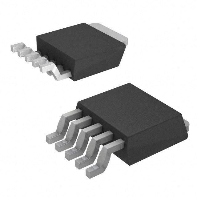
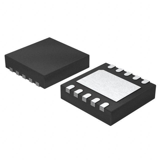
| 供应商器件封装 | 6-UMLP(2x2) |
| 其它名称 | FAN4860UMP5XCT |
| 包装 | 剪切带 (CT) |
| 单位重量 | 40 mg |
| 同步整流器 | 是 |
| 商标 | Fairchild Semiconductor |
| 安装类型 | 表面贴装 |
| 安装风格 | SMD/SMT |
| 封装 | Reel |
| 封装/外壳 | 6-UDFN 裸露焊盘 |
| 封装/箱体 | MLP-6 |
| 工作温度 | -40°C ~ 85°C |
| 工厂包装数量 | 3000 |
| 开关频率 | 3 MHz |
| 最大工作温度 | + 85 C |
| 最大输入电压 | 4.5 V |
| 最小工作温度 | - 40 C |
| 最小输入电压 | 2.3 V |
| 标准包装 | 1 |
| 电压-输入 | 2.3 V ~ 4.5 V |
| 电压-输出 | 5V |
| 电流-输出 | 200mA |
| 类型 | Voltage Converter |
| 系列 | FAN4860 |
| 输出数 | 1 |
| 输出电压 | 5 V |
| 输出电流 | 300 mA |
| 输出端数量 | 1 Output |
| 输出类型 | 固定 |
| 频率-开关 | 3MHz |


- 商务部:美国ITC正式对集成电路等产品启动337调查
- 曝三星4nm工艺存在良率问题 高通将骁龙8 Gen1或转产台积电
- 太阳诱电将投资9.5亿元在常州建新厂生产MLCC 预计2023年完工
- 英特尔发布欧洲新工厂建设计划 深化IDM 2.0 战略
- 台积电先进制程称霸业界 有大客户加持明年业绩稳了
- 达到5530亿美元!SIA预计今年全球半导体销售额将创下新高
- 英特尔拟将自动驾驶子公司Mobileye上市 估值或超500亿美元
- 三星加码芯片和SET,合并消费电子和移动部门,撤换高东真等 CEO
- 三星电子宣布重大人事变动 还合并消费电子和移动部门
- 海关总署:前11个月进口集成电路产品价值2.52万亿元 增长14.8%


PDF Datasheet 数据手册内容提取
Is Now Part of To learn more about ON Semiconductor, please visit our website at www.onsemi.com Please note: As part of the Fairchild Semiconductor integration, some of the Fairchild orderable part numbers will need to change in order to meet ON Semiconductor’s system requirements. Since the ON Semiconductor product management systems do not have the ability to manage part nomenclature that utilizes an underscore (_), the underscore (_) in the Fairchild part numbers will be changed to a dash (-). This document may contain device numbers with an underscore (_). Please check the ON Semiconductor website to verify the updated device numbers. The most current and up-to-date ordering information can be found at www.onsemi.com. Please email any questions regarding the system integration to Fairchild_questions@onsemi.com. ON Semiconductor and the ON Semiconductor logo are trademarks of Semiconductor Components Industries, LLC dba ON Semiconductor or its subsidiaries in the United States and/or other countries. ON Semiconductor owns the rights to a number of patents, trademarks, copyrights, trade secrets, and other intellectual property. A listing of ON Semiconductor’s product/patent coverage may be accessed at www.onsemi.com/site/pdf/Patent-Marking.pdf. ON Semiconductor reserves the right to make changes without further notice to any products herein. ON Semiconductor makes no warranty, representation or guarantee regarding the suitability of its products for any particular purpose, nor does ON Semiconductor assume any liability arising out of the application or use of any product or circuit, and specifically disclaims any and all liability, including without limitation special, consequential or incidental damages. Buyer is responsible for its products and applications using ON Semiconductor products, including compliance with all laws, regulations and safety requirements or standards, regardless of any support or applications information provided by ON Semiconductor. “Typical” parameters which may be provided in ON Semiconductor data sheets and/or specifications can and do vary in different applications and actual performance may vary over time. All operating parameters, including “Typicals” must be validated for each customer application by customer’s technical experts. ON Semiconductor does not convey any license under its patent rights nor the rights of others. ON Semiconductor products are not designed, intended, or authorized for use as a critical component in life support systems or any FDA Class 3 medical devices or medical devices with a same or similar classification in a foreign jurisdiction or any devices intended for implantation in the human body. Should Buyer purchase or use ON Semiconductor products for any such unintended or unauthorized application, Buyer shall indemnify and hold ON Semiconductor and its officers, employees, subsidiaries, affiliates, and distributors harmless against all claims, costs, damages, and expenses, and reasonable attorney fees arising out of, directly or indirectly, any claim of personal injury or death associated with such unintended or unauthorized use, even if such claim alleges that ON Semiconductor was negligent regarding the design or manufacture of the part. ON Semiconductor is an Equal Opportunity/Affirmative Action Employer. This literature is subject to all applicable copyright laws and is not for resale in any manner.
F A N 4 8 6 February 2014 0 — 3 M H z , FAN4860 S y n 3 MHz, Synchronous TinyBoost™ Regulator c h r o n Features Description o u Operates with Few External Components: 1 H Inductor The FAN4860 is a low-power boost regulator designed to s T and 0402 Case Size Input and Output Capacitors provide a regulated 3.3 V, 5.0 V or 5.4 V output from a single i n Input Voltage Range from 2.3 V to 5.4 V cell Lithium or Li-Ion battery. Output voltage options are fixed y at 3.3 V, 5.0 V, or 5.4 V with a guaranteed maximum load B Fixed 3.3 V, 5.0 V, or 5.4 V Output Voltage Options current of 200 mA at V =2.3 V and 300 mA at V =3.3 V. o IN IN o Maximum Load Current >150 mA at VIN=2.3 V Imnpauxitm cizuerrse bnat titne ryS hlifuet.d own Mode is less than 1 µA, which st™ Maximum Load Current 300 mA at VIN=3.3 V, VOUT=5.4 V Light-load PFM operation is automatic and “glitch-free”. The R Maximum Load Current 300 mA at VIN=3.3 V, VOUT=5.0 V regulator maintains output regulation at no-load with as low eg Maximum Load Current 300 mA at V =2.7 V, V =3.3 V as 37 µA quiescent current. u IN OUT l a Up to 92% Efficient The combination of built-in power transistors, synchronous to rectification, and low supply current make the FAN4860 ideal r Low Operating Quiescent Current for battery powered applications. True Load Disconnect During Shutdown The FAN4860 is available in 6-bump 0.4 mm pitch Wafer- Variable On-time Pulse Frequency Modulation (PFM) with Level Chip Scale Package (WLCSP) and a 6-lead 2x2 mm ultra-thin MLP package. Light-Load Power-Saving Mode Internal Synchronous Rectifier (No External Diode Needed) Thermal Shutdown and Overload Protection 6-Pin 2 x 2 mm UMLP 6-Bump WLCSP, 0.4 mm Pitch Applications USB “On the Go” 5 V Supply 5 V Supply – HDMI, H-Bridge Motor Drivers Figure 1. Typical Application Powering 3.3 V Core Rails PDAs, Portable Media Players Cell Phones, Smart Phones, Portable Instruments Ordering Information Part Number Operating Temperature Range Package Packing Method FAN4860UC5X -40°C to 85°C WLCSP, 0.4 mm Pitch Tape and Reel FAN4860UMP5X -40°C to 85°C UMLP-6, 2 x 2 mm Tape and Reel FAN4860UC33X -40°C to 85°C WLCSP, 0.4 mm Pitch Tape and Reel FAN4860UC54X -40°C to 85°C WLCSP, 0.4 mm Pitch Tape and Reel © 2010 Fairchild Semiconductor Corporation www.fairchildsemi.com FAN4860 • Rev. 1.1.1
F A Block Diagrams N 4 8 6 0 — 3 M H z , S y n c h r o n o u s T i n y B o o s t Figure 2. IC Block Diagram ™ R e g Pin Configurations u l a t o r Figure 3. WLCSP (Top View) Figure 4. WLCSP (Bottom View) Figure 5. 2x2 mm UMLP (Top View) Pin Definitions Pin # Name Description WLCSP UMLP A1 6 VIN Input Voltage. Connect to Li-Ion battery input power source and input capacitor (C ). IN B1 5 SW Switching Node. Connect to inductor. C1 4 EN Enable. When this pin is HIGH, the circuit is enabled. This pin should not be left floating. C2 3 FB Feedback. Output voltage sense point for V . Connect to output capacitor (C ). OUT OUT B2 2 VOUT Output Voltage. This pin is both the output voltage terminal as well as an IC bias supply. Ground. Power and signal ground reference for the IC. All voltages are measured with A2 1, P1 GND respect to this pin. © 2010 Fairchild Semiconductor Corporation www.fairchildsemi.com FAN4860 • Rev. 1.1.1 2
F A N Absolute Maximum Ratings 4 8 6 Stresses exceeding the absolute maximum ratings may damage the device. The device may not function or be operable 0 above the recommended operating conditions and stressing the parts to these levels is not recommended. In addition, — extended exposure to stresses above the recommended operating conditions may affect device reliability. The absolute 3 maximum ratings are stress ratings only. M H Symbol Parameter Min. Max. Units z , S V VIN Pin -0.3 5.5 V IN y n V VOUT Pin –2 6 V OUT c h VFB FB Pin –2 6 V r o DC -0.3 5.5 n V SW Node V o SW Transient: 10 ns, 3 MHz -1.0 6.5 u s VEN EN Pin -0.3 5.5 V T i Electrostatic Discharge Human Body Model per JESD22-A114 2 n ESD kV y Protection Level Charged Device Model per JESD22-C101 1 B o T Junction Temperature –40 +150 °C o J s TSTG Storage Temperature –65 +150 °C t™ TL Lead Soldering Temperature, 10 Seconds +260 °C R e g u l a Recommended Operating Conditions t o r The Recommended Operating Conditions table defines the conditions for actual device operation. Recommended operating conditions are specified to ensure optimal performance to the datasheet specifications. Fairchild does not recommend exceeding them or designing to absolute maximum ratings. Symbol Parameter Min. Max. Units 5.4 V 2.3 4.5 OUT V Supply Voltage 5.0 V 2.3 4.5 V IN OUT 3.3 V 2.3 3.2 OUT I Output Current 200 mA OUT T Ambient Temperature –40 +85 °C A T Junction Temperature –40 +125 °C J Thermal Properties Junction-to-ambient thermal resistance is a function of application and board layout. This data is measured with four-layer 2s2p boards in accordance to JEDEC standard JESD51. Special attention must be paid not to exceed junction temperature T at a given ambient temperate T . J(max) A Symbol Parameter Typical Units WLCSP 130 °C/W Junction-to-Ambient Thermal Resistance JA UMLP 57 °C/W © 2010 Fairchild Semiconductor Corporation www.fairchildsemi.com FAN4860 • Rev. 1.1.1 3
F A N Electrical Specifications 4 8 6 Minimum and maximum values are at VIN=VEN=2.3 V to 4.5 V (2.5 to 3.2 VIN for 3.3 VOUT option), TA=-40°C to +85°C; 0 circuit of Figure 1, unless otherwise noted. Typical values are at TA=25°C, VIN=VEN=3.6 V for VOUT=5.0 V / 5.4 V, and — VIN=VEN=2.7 V for VOUT=3.3 V. 3 M Symbol Parameter Conditions Min. Typ. Max. Units H Quiescent: V =3.6 V, I =0, EN=V 37 45 z IN OUT IN , 5.4 V OUT S Shutdown: EN=0, V =3.6 V 0.5 1.5 IN y n Quiescent: V =3.6 V, I =0, EN=V 37 45 I V Input Current 5.0 V IN OUT IN A c IN IN OUT h Shutdown: EN=0, V =3.6 V 0.5 1.5 IN r o Quiescent: VIN=2.7 V, IOUT=0, EN=VIN 50 65 n 3.3 VOUT o Shutdown: EN=0, VIN=2.7 V 0.5 1.5 u s ILK_OUT VOUT Leakage Current VOUT=0, EN=0, VIN≥3 V 10 nA T VOUT=5.4 V, VIN=3.6 V, EN=0 in y ILK_RVSR VOUT to VIN Reverse Leakage VOUT=5.0 V, VIN=3.6 V, EN=0 2.5 A B V =3.3 V, V =3.0 V, EN=0 o OUT IN o V Under-Voltage Lockout V Rising 2.2 2.3 V s UVLO IN t ™ V UVLO_HY Under-Voltage Lockout Hysteresis 190 mV R S e VENH Enable HIGH Voltage 1.05 V g u VENL Enable LOW Voltage 0.4 V la ILK_EN Enable Input Leakage Current 0.01 1.00 A to r V from 2.3 V to 4.5 V, I ≤200 mA 5.15 5.40 5.50 IN OUT 5.4 V V from 2.7 V to 4.5 V, I ≤200 mA 5.20 5.40 5.50 OUT IN OUT V from 3.3 V to 4.5 V, I ≤300 mA 5.15 5.40 5.50 IN OUT Output Voltage V V from 2.3 V to 4.5 V, I ≤200 mA 4.80 5.05 5.15 V OUT Accuracy(1) IN OUT 5.0 V V from 2.7 V to 4.5 V, I ≤200 mA 4.85 5.05 5.15 OUT IN OUT V from 3.3 V to 4.5 V, I ≤300 mA 4.85 5.05 5.15 IN OUT 3.3 V V from 2.5 V to 3.2 V, I ≤200 mA 3.17 3.33 3.41 OUT IN OUT Referred to V =5.4 V 5.325 5.400 5.475 OUT V Reference Accuracy Referred to V =5.0 V 4.975 5.050 5.125 V REF OUT Referred to V =3.3 V 3.280 3.330 3.380 OUT V =3.6 V, V =5.4 V, I =200 mA 185 230 255 IN OUT OUT t Off Time V =3.6 V, V =5.0 V, I =200 mA 195 240 265 ns OFF IN OUT OUT V =2.7 V, V =3.3 V, I =200 mA 240 290 350 IN OUT OUT V =2.3 V 200 IN 5.4 V V =3.3 V 300 OUT IN V =3.6 V 400 IN Maximum Output VIN=2.3 V 200 I mA OUT Current(1) 5.0 V V =3.3 V 300 OUT IN V =3.6 V 400 IN V =2.5 V 250 IN 3.3 V OUT V =2.7 V 300 IN 5.4 V V =3.6 V, V >V 1000 1400 1500 OUT IN OUT IN SW Peak Current I 5.0 V V =3.6 V, V >V 930 1100 1320 mA SW Limit OUT IN OUT IN 3.3 V V =2.7 V, V >V 650 800 950 OUT IN OUT IN Continued on the following page… © 2010 Fairchild Semiconductor Corporation www.fairchildsemi.com FAN4860 • Rev. 1.1.1 4
F A N Electrical Specifications 4 8 6 Minimum and maximum values are at VIN=VEN=2.3 V to 4.5 V (2.5 to 3.2 VIN for 3.3 VOUT option), TA=-40°C to +85°C; 0 circuit of Figure 1, unless otherwise noted. Typical values are at TA=25°C, VIN=VEN=3.6 V for VOUT=5.0 V / 5.4 V, and — VIN=VEN=2.7 V for VOUT=3.3 V. 3 M Symbol Parameter Conditions Min. Typ. Max. Units H 5.4 V V =3.6 V, V < V 900 z OUT IN OUT IN , Soft-Start Input Peak S I 5.0 V V =3.6 V, V < V 850 mA SS Current Limit(2) OUT IN OUT IN y n 3.3 V V =2.7 V, V < V 700 OUT IN OUT IN c 5.4 V V =3.6 V, I =200 mA 270 400 h OUT IN OUT r tSS Soft-Start Time(3) 5.0 VOUT VIN=3.6 V, IOUT=200 mA 100 300 s on o 3.3 VOUT VIN=2.7 V, IOUT=200 mA 250 750 u s N-Channel Boost Switch V =3.6 V 300 R IN mΩ T DS(ON) P-Channel Sync Rectifier VIN=3.6 V 400 in y T Thermal Shutdown I =10 mA 150 °C TSD LOAD B T Thermal Shutdown Hysteresis 30 °C o TSD_HYS o Notes: s t 1. I from 0 to I ; also includes load transient response. V measured from mid-point of output voltage ripple. ™ LOAD OUT OUT Effective capacitance of COUT > 1.5 F. R 2. Guaranteed by design and characterization; not tested in production. e 3. Elapsed time from rising EN until regulated V g OUT. u l a to r © 2010 Fairchild Semiconductor Corporation www.fairchildsemi.com FAN4860 • Rev. 1.1.1 5
F A N 4 5.4 V Typical Characteristics 8 OUT 6 0 Unless otherwise specified; circuit per Figure 1, 3.6 VIN, and TA=25°C. — 3 M 94.00% H 96.00% z 92.00% , 94.00% S y 92.00% 90.00% n Efficiency (%) 889680...000000%%% Efficiency (%) 8868..0000%% +25(cid:1320) chronous 84.00% 43..56VViinn 84.00% ‐+4805(cid:1320)(cid:1320) T 82.00% 3.2Vin in 2.5Vin 82.00% y B 80.00% 0 50 100 150 200 250 300 0 50 100 150 200 250 300 Load Current (mA) o Load Current (mA) o s t ™ Figure 6. Efficiency vs. V Figure 7. Efficiency vs. Temperature, 3.6 V IN IN R e g 5.44 100 u l 5.42 90 a t 5.4 μA) 80 ‐40(cid:1320) or Vout(V) 5555....33332468 (escent current 567000 2855(cid:1320)(cid:1320) 5.3 Iout (mA) @Vin=4.5V ui 40 Q 5.28 Iout (mA) @Vin=3.6V 30 Iout (mA) @Vin=3.2V 5.26 Iout (mA) @ Vin=2.5V 20 5.24 2 2.5 3 3.5 4 4.5 5 0 50 100 150 200 250 300 Input voltage (V) Iload(mA) Figure 8. Line and Load Regulation Figure 9. Quiescent Current 1000 1800 900 1700 mA) 800 mA) 1600 d Current, max, ( 567000000 8‐24550(cid:1320)(cid:1320)(cid:1320) Peak Inductor Current ( 1111234500000000 a o 400 L 1100 25(cid:1320) 300 1000 2 2.5 3 3.5 4 4.5 200 2 2.5 3 3.5 4 4.5 Input Voltage (V) Input voltage (V) Figure 10. Maximum DC Load Current Figure 11. Peak Inductor Current © 2010 Fairchild Semiconductor Corporation www.fairchildsemi.com FAN4860 • Rev. 1.1.1 6
F A N 5.4 V Typical Characteristics 4 OUT 8 6 Unless otherwise specified; circuit per Figure 1, 3.6 VIN, and TA=25°C. 0 — 3 M H z , S y n c h r o n o u s T i n y B o Figure 12. 0-50 mA Load Transient, 100 ns Step Figure 13. 50-200 mA Load Transient, 100 ns Step o s t ™ R e g u l a t o r Figure 14. Line Transient, 5 mA Load, 10 µs Step Figure 15. Line Transient, 200 mA Load, 10 µs Step 5.0 V Typical Characteristics OUT Unless otherwise specified; circuit per Figure 1, 3.6 V , and T =25°C. IN A 100 95 95 92 %) Efficiency (%) 8950 Efficiency ( 8869 80 23..53 VViinn 83 -40C 3.6 Vin +25C 4.5 Vin +85C 75 80 0 50 100 150 200 250 300 0 50 100 150 200 250 300 Load Current (mA) Load Current (mA) Figure 16. Efficiency vs. V Figure 17. Efficiency vs. Temperature, 3.6 V IN IN © 2010 Fairchild Semiconductor Corporation www.fairchildsemi.com FAN4860 • Rev. 1.1.1 7
F A N 4 5.0 V Typical Characteristics 8 OUT 6 0 Unless otherwise specified; circuit per Figure 1, 3.6 VIN, and TA=25°C. — 3 50 50 M 2.5 Vin -40C H 3.3 Vin +25C z 25 3.6 Vin 25 +85C , 4.5 Vin S y V) 0 V) 0 n m m UT -5.05V ( -25 UT -5.05V ( -25 chron VO -50 VO -50 o u s -75 -75 T i n -100 -100 y B 0 50 100 150 200 250 300 0 50 100 150 200 250 300 o Load Current (mA) Load Current (mA) o s Figure 18. Line and Load Regulation Figure 19. Load Regulation vs. Temperature, 3.6 VIN t™ R 4000 e 50 g -40C u +25C la 3200 45 +85C t o Frequency (KHz) 12640000 uiescent Current (uA) 3450 r Q 30 800 2.5 Vin 3.6 Vin 4.5 Vin 25 0 2.0 2.5 3.0 3.5 4.0 4.5 5.0 0 50 100 150 200 250 300 Input Voltage(V) Load Current (mA) Figure 20. Switching Frequency Figure 21. Quiescent Current Figure 22. Maximum DC Load Current Figure 23. Peak Inductor Current © 2010 Fairchild Semiconductor Corporation www.fairchildsemi.com FAN4860 • Rev. 1.1.1 8
F A N 4 5.0 V Typical Characteristics 8 OUT 6 0 Unless otherwise specified; circuit per Figure 1, 3.6 VIN, and TA=25°C. — 3 M H z , S y n c h r o n o u s T i n y B o o s Figure 24. Output Ripple, 10 mA PFM Load Figure 25. Output Ripple, 200 mA PWM Load t ™ R e g u l a t o r Figure 26. 0-50 mA Load Transient, 100 ns Step Figure 27. 50-200 mA Load Transient, 100 ns Step Figure 28. Line Transient, 5 mA Load, 10 µs Step Figure 29. Line Transient, 200 mA Load, 10 µs Step © 2010 Fairchild Semiconductor Corporation www.fairchildsemi.com FAN4860 • Rev. 1.1.1 9
F A N 4 5.0 V Typical Characteristics 8 OUT 6 0 Unless otherwise specified; circuit per Figure 1, 3.6 VIN, and TA=25°C. — 3 M H z , S y n c h r o n o u s T i n y B o o s Figure 30. Startup, No Load Figure 31. Startup, 33 Load t ™ R e g u l a t o r Figure 32. Shutdown, 1 k Load Figure 33. Shutdown, 33 Load Figure 34. Overload Protection Figure 35. Short-Circuit Response © 2010 Fairchild Semiconductor Corporation www.fairchildsemi.com FAN4860 • Rev. 1.1.1 10
F A N 4 3.3 V Typical Characteristics 8 OUT 6 0 Unless otherwise specified; circuit per Figure 1, 3.0 VIN, and TA=25°C. — 3 M 100 98 H z , 95 95 S y n %) 90 92 c Efficiency ( 85 Efficiency (%) 89 hrono u 80 22..57 VViinn 86 -40C s 3.0 Vin +25C T 3.2 Vin +85C in 75 83 y 0 50 100 150 200 250 300 0 50 100 150 200 250 300 B Load Current (mA) Load Current (mA) o o s Figure 36. Efficiency vs. VIN Figure 37. Efficiency vs. Temperature, 3.0 VIN t™ R e 40 40 g 2.5 Vin -40C u 20 23..70 VViinn 20 ++2855CC lat 3.2 Vin o mV) 0 mV) 0 r V ( V ( 3.33 -20 3.33 -20 T - T - U U VO -40 VO -40 -60 -60 -80 -80 0 50 100 150 200 250 300 0 50 100 150 200 250 300 Load Current (mA) Load Current (mA) Figure 38. Line and Load Regulation Figure 39. Load Regulation vs. Temperature, 3.0 V IN 55 700 50 mA) 600 nt Current (uA) 4405 DC Load Current ( 450000 Quiesce 35 -40C Maximum 300 -40C +25C +25C +85C +85C 30 200 2.0 2.3 2.6 2.9 3.2 3.5 2.0 2.3 2.6 2.9 3.2 3.5 Input Voltage(V) Input Voltage(V) Figure 40. Quiescent Current Figure 41. Maximum DC Load Current © 2010 Fairchild Semiconductor Corporation www.fairchildsemi.com FAN4860 • Rev. 1.1.1 11
F A N 4 3.3 V Typical Characteristics 8 OUT 6 0 Unless otherwise specified; circuit per Figure 1, 3.0 VIN, and TA=25°C. — 3 M H z , S y n c h r o n o u s T i n y B o o s Figure 42. Output Ripple, 10 mA PFM Load Figure 43. Output Ripple, 200 mA PWM Load t ™ R e g u l a t o r Figure 44. Startup, No Load Figure 45. Startup, 22 Load © 2010 Fairchild Semiconductor Corporation www.fairchildsemi.com FAN4860 • Rev. 1.1.1 12
F A N 4 Functional Description 8 6 0 Circuit Description PFM Mode — 3 The FAN4860 is a synchronous boost regulator, typically If VOUT > VREF when the minimum off-time has ended, the M operating at 3 MHz in Continuous Conduction Mode regulator enters PFM Mode. Boost pulses are inhibited until H (CCM), which occurs at moderate to heavy load current VOUT < VREF. The minimum on-time is increased to enable z , and low VIN voltages. the output to pump up sufficiently with each PFM boost S pulse. Therefore, the regulator behaves like a constant on- y At light-load currents, the converter switches automatically to n time regulator, with the bottom of its output voltage ripple at power-saving PFM Mode. The regulator automatically and c 5.05 V in PFM Mode. h smoothly transitions between quasi-fixed-frequency r o continuous conduction PWM Mode and variable-frequency Table 1. Operating States n PFM Mode to maintain the highest possible efficiency over o the full range of load current and input voltage. Mode Description Invoked When: u s PWM Mode Regulation LIN Linear Startup VIN > VOUT T i SS Boost Soft-Start V < V n The FAN4860 uses a minimum on-time and computed OUT REG y B minimum off-time to regulate VOUT. The regulator achieves BST Boost Operating Mode VOUT=VREG o excellent transient response by employing current mode o Shutdown and Startup s modulation. This technique causes the regulator output to t exhibit a load line. During PWM Mode, the output voltage If EN is LOW, all bias circuits are off and the regulator is in ™ drops slightly as the input current rises. With a constant VIN, Shutdown Mode. During shutdown, true load disconnect R this appears as a constant output resistance. between battery and load prevents current flow from VIN to e V , as well as reverse flow from V to V . g The “droop” caused by the output resistance when a load is OUT OUT IN u l applied allows the regulator to respond smoothly to load LIN State a t transients with negligible overshoot. When EN rises, if V > UVLO, the regulator first attempts to o IN r bring V within about 1V of V by using the internal fixed 700 OUT IN 3.3 Vout current source from VIN (ILIN1). The current is limited to about 630 mA during LIN1 Mode. 5.0 Vout 600 If V reaches V -1V during LIN1 Mode, the SS state is m) 500 initiaOtUeTd. OtherwiseIN, LIN1 times out after 16 clock counts and e ( the LIN2 Mode is entered. c n a sist 400 In LIN2 Mode, the current source is incremented to 850 mA. Re If V fails to reach V -1 V after 64 clock counts, a fault ut OUT IN utp 300 condition is declared. O SS State 200 Upon the successful completion of the LIN state (V >V - OUT IN 1 V), the regulator begins switching with boost pulses current 100 limited to about 50% of nominal level, incrementing to full 2.0 2.5 3.0 3.5 4.0 4.5 5.0 scale over a period of 32 clock counts. Input Voltage (V) Figure 46. Output Resistance (ROUT) If the output fails to achieve 90% of its set point within 96 clock counts at full-scale current limit, a fault condition is declared. When the regulator is in PWM CCM Mode and the target VOUT = 5.05 V, VOUT is a function of ILOAD and can be BST State computed as: This is the normal operating mode of the regulator. The regulator uses a minimum t -minimum t modulation VOUT 5.05ROUTILOAD (1) OFF VIN ON scheme. Minimum tOFF is proportional to VOUT, which keeps For example, at VIN=3.3 V, and ILOAD=200 mA, VOUT drops to: the regulator’s switching frequency reasonably constant in CCM. t is proportional to V and is higher if the inductor VOUT 5.050.380.24.974V (1A) current OrNe(aMcINh)es 0 before t IdNuring the prior cycle. OFF(MIN) At VIN=2.3 V, and ILOAD=200 mA, VOUT drops to: To ensure that VOUT does not pump significantly above the regulation point, the boost switch remains off as long as VOUT 5.050.680.24.914V (1B) FB > VREF. © 2010 Fairchild Semiconductor Corporation www.fairchildsemi.com FAN4860 • Rev. 1.1.1 13
F A Fault State The V -dependent LIN Mode charging current is illustrated N IN 4 in Figure 49. 8 The regulator enters the FAULT state under any of the 6 following conditions: 0 — V fails to achieve the voltage required to advance from OUT LIN state to SS state. 3 M V fails to achieve the voltage required to advance from H OUT z SS state to BST state. , S Sustained (32 CLK counts) pulse-by-pulse current limit y during the BST state. n c The regulator moves from BST to LIN state due to a short h r circuit or output overload (V < V -1 V). o OUT IN n Once a fault is triggered, the regulator stops switching and o u presents a high-impedance path between V and V . After IN OUT s waiting 480 CLK counts, a restart is attempted. T i Figure 49. LIN Mode Current vs. VIN ny B Soft-Start and Fault Timing o o s The soft-start timing for each state, and the fault times, are Over-Temperature Protection (OTP) t ™ determined by the fault clock, whose period is inversely proportional to V . This allows the regulator more time to The regulator shuts down when the thermal shutdown R IN charge larger values of C when V is lower. With higher threshold is reached. Restart, with soft-start, occurs when e OUT IN g VIN, this also reduces power delivered to VOUT during each the IC has cooled by about 30°C. u cycle in current limit. la t o The number of clock counts for each state is illustrated in Over-Current Protection (OCP) r Figure 47. During Boost Mode, the FAN4860 employs a cycle-by-cycle peak current limit to protect switching elements. Sustained current limit, for 32 consecutive fault clock counts, initiates a fault condition. During an overload condition, as V collapses to OUT approximately V -1 V, the synchronous rectifier is IN immediately switched off and a fault condition is declared. Automatic restart occurs once the overload/short is removed and the fault timer completes counting. Figure 47. Fault Response into Short Circuit The fault clock period as a function of V is shown in Figure 48. IN Figure 48. Fault Clock Period vs. V IN © 2010 Fairchild Semiconductor Corporation www.fairchildsemi.com FAN4860 • Rev. 1.1.1 14
F A Application Information N 4 8 External Component Selection CEFF varies with manufacturer, dielectric material, case size, 6 0 and temperature. Some manufacturers may be able to Table 2 shows the recommended external components for provide an X5R capacitor in 0402 case size that retains C — EFF the FAN4860: >1.5 F with 5V bias; others may not. If this CEFF cannot be 3 economically obtained and 0402 case size is required, the IC M Table 2. External Components H can work with the 0402 capacitor as long as the minimum z REF Description Manufacturer VIN is restricted to >2.7 V. , S 1.0 µH, 0.8 A, Murata LQM21PN1R0MC0, For best performance, a 10 V-rated 0603 output capacitor is y L1 recommended (Kemet C0603C475K8PAC, or equivalent). n 190 m, 0805 or equivalent c Since it retains greater CEFF under bias and over h 2.2 µF, 6.3 V, X5R, Murata GRM155R60J225M temperature, output ripple can is reduced and transient r C o IN 0402 TDK C1005X5R0J225M capability enhanced. n o C 4.7 µF, 10 V, X5R, Kemet C0603C475K8PAC Output Voltage Ripple us OUT 0603(4) TDK C1608X5R1A475K Output voltage ripple is inversely proportional to C . T OUT i Note: During tON, when the boost switch is on, all load current is ny 4. A 6.3 V-rated 0603 capacitor may be used for COUT, supplied by COUT. B such as Murata GRM188R60J225M. All datasheet I o parameters are valid with the 6.3 V-rated capacitor. VRIPPLE(PP) tONCLOAD (2) os Due to DC bias effects, the 10 V capacitor offers a OUT t ™ performance enhancement; particularly output ripple and and transient response, without any size increase. R t t Dt 1 VIN e ON SW SW VOUT (3) gu Output Capacitance (COUT) Therefore: la t SThtaeb ieliftfeyc tive capacitance (CEFF) of small, high-value, VRIPPLE(PP) tSW 1 VVOIUNT CILOOAUDT (4) or ceramic capacitors decrease as their bias voltage increases, as shown in Figure 50. where: tSW 1f (5) SW As can be seen from Equation 4, the maximum V RIPPLE occurs when V is minimum and I is maximum. IN LOAD Startup Input current limiting is in effect during soft-start, which limits the current available to charge C . If the output fails to OUT achieve regulation within the time period described in the soft-start section above; a FAULT occurs, causing the circuit to shut down, then restart after a significant time period. If C is a very high value, the circuit may not start on the first OUT attempt, but eventually achieves regulation if no load is present. If a high-current load and high capacitance are both present during soft-start, the circuit may fail to achieve Figure 50. CEFF for 4.7 F, 0603, X5R, 6.3 V regulation and continually attempt soft-start, only to have (Murata GRM188R60J475K) C discharged by the load when in the FAULT state. OUT The circuit can start with higher values of C under full OUT FAN4860 is guaranteed for stable operation with the load if V is higher, since: IN minimum value of C (C ) outlined in Table 3. EFF EFF(MIN) I V Table 3. Minimum C Required for Stability IOUT ILIM(PK) RIPPLE IN (6) EFF 2 VOUT Operating Conditions C (F) EFF(MIN) Generally, the limitation occurs in BST Mode. V (V) I (mA) IN LOAD 2.3 to 4.5 0 to 200 1.5 2.7 to 4.5 0 to 200 1.0 2.3 to 4.5 0 to 150 1.0 © 2010 Fairchild Semiconductor Corporation www.fairchildsemi.com FAN4860 • Rev. 1.1.1 15
F A The FAN4860 starts on the first pass (without triggering a Layout Guideline N 4 FAULT) under the following conditions for C : EFF(MAX) 8 6 Table 4. Maximum C for First-Pass Startup 0 EFF — Operating Conditions 3 R (Ω) C (F) M V (V) LOAD(MIN) EFF(MAX) H IN 5.4 V 5.0 V 3.3 V z OUT OUT OUT , S > 2.3 27 25 16 10 y n > 2.7 27 25 16 15 c h > 2.7 37 33 20 22 r o C values shown in Table 4 typically apply to the lowest n EFF o V . The presence of higher V enhances ability to start into IN IN u larger CEFF at full load. s T i n Transient Protection y Figure 52. WLCSP Suggested Layout (Top View) B o To protect against external voltage transients caused by o ESD discharge events, or improper external connections, s some applications employ an external transient voltage t™ suppressor (TVS) and Schottky diode (D1 in Figure 51). R e g u l a t o r S V T Figure 51. FAN4860 with External Transient Protection The TVS is designed to clamp the FB line (system V ) to OUT +10 V or –2 V during external transient events. The Schottky Figure 53. UMLP Suggested Layout (Top View) diode protects the output devices from the positive excursion. The FB pin can tolerate up to 14 V of positive excursion, while both the FB and VOUT pins can tolerate negative voltages. The FAN4860 includes a circuit to detect a missing or defective D1 by comparing V to FB. If V – FB > about OUT OUT 0.7 V, the IC shuts down. The IC remains shut down until V < UVLO and V < UVLO+0.7 or EN is toggled. OUT IN C may be necessary to preserve load transient response OUT2 when the Schottky is used. When a load is applied at the FB pin, the forward voltage of the D1 rapidly increases before the regulator can respond or the inductor current can change. This causes an immediate drop of up to 300 mV, depending on D1’s characteristics if C is absent. C OUT2 OUT2 supplies instantaneous current to the load while the regulator adjusts the inductor current. A value of at least half of the minimum value of C should be used for C . C OUT OUT2 OUT2 needs to withstand the maximum voltage at the FB pin as the TVS is clamping. The maximum DC output current available is reduced with this circuit, due to the additional dissipation of D1. © 2010 Fairchild Semiconductor Corporation www.fairchildsemi.com FAN4860 • Rev. 1.1.1 16
F A Physical Dimensions N 4 8 6 F 0 0.03 C — 2X E A 3 B 0.40 M BALL A1 A1 H (Ø0.20) INDEX AREA Cu Pad z, S 0.40 D F y (Ø0.30) n Solder Mask c 0.03 C Opening hr 2X o n o TOP VIEW RECOMMENDED LAND PATTERN u s (NSMD PAD TYPE) T i n 0.06 C y 0.378±0.018 B 0.625 0.05 C 0.547 E 0.208±0.021 oo s t ™ C SEATING PLANE R D e g u SIDE VIEWS l a t o r Ø0.260±0.010 NOTES: 6X 0.40 0.005 C A B A. NO JEDEC REGISTRATION APPLIES. B. DIMENSIONS ARE IN MILLIMETERS. C B (Y) +/-0.018 C. DIMENSIONS AND TOLERANCES PER 0.40 ASMEY14.5M, 1994. A D. DATUM C, THE SEATING PLANE IS DEFINED 1 2 F BY THE SPHERICAL CROWNS OF THE BALLS. (X) +/-0.018 E. PACKAGE TYPICAL HEIGHT IS 586 MICRONS BOTTOM VIEW ±39 MICRONS (547-625 MICRONS). F. FOR DIMENSIONS D, E, X, AND Y SEE PRODUCT DATASHEET. G. DRAWING FILENAME: UC006ACrev4. Figure 54. 6-Lead, 0.4 mm Pitch, WLCSP Package Product-Specific Dimensions Product D E X Y FAN4860UC5X 1.230mm ±0.030 mm 0.880 mm ±0.030 mm 0.240 mm 0.215 mm FAN4860UC33X Package drawings are provided as a service to customers considering Fairchild components. Drawings may change in any manner without notice. Please note the revision and/or date on the drawing and contact a Fairchild Semiconductor representative to verify or obtain the most recent revision. Package specifications do not expand the terms of Fairchild’s worldwide terms and conditions, specifically the warranty therein, which covers Fairchild products. Always visit Fairchild Semiconductor’s online packaging area for the most recent package drawings: http://www.fairchildsemi.com/dwg/UC/UC006AC.pdf. © 2010 Fairchild Semiconductor Corporation www.fairchildsemi.com FAN4860 • Rev. 1.1.1 17
F A N Physical Dimensions 4 8 6 0 — 0.10 C 2.0 A 3 2X M H B z , S y 1.45 n c 2.0 h (0.25) r o n o PIN1 u IDENT 0.10 C 0.80 1.80 s 2X T i n 6X 0.50 TOP VIEW y B 0.65 o 6X 0.35 o s 0.55 MAX A t™ 0.10 C (0.15) RECOMMENDED LAND PATTERN R e g 0.08 C u l 0.05 C a 0.00 to r SEATING PLANE SIDE VIEW NOTES: 1.35 A. PACKAGE CONFORMS TO JEDEC MO-229 1.45 EXCEPT WHERE NOTED. PIN1 1 3 B. DIMENSIONS ARE IN MILLIMETERS. IDENT C. DIMENSIONS AND TOLERANCES PER 0.70 ASME Y14.5M, 1994. 6X0.35 0.80 D. LANDPATTERN RECOMMENDATION IS BASED 0.25 ON FSC DESIGN ONLY. 0.10 C A B 6 4 E. DRAWING FILENAME: MKT-UMLP06Erev2. 0.05 C 0.35 0.65 6X 0.25 BOTTOM VIEW Figure 55. 6-Lead, UMLP Package Package drawings are provided as a service to customers considering Fairchild components. Drawings may change in any manner without notice. Please note the revision and/or date on the drawing and contact a Fairchild Semiconductor representative to verify or obtain the most recent revision. Package specifications do not expand the terms of Fairchild’s worldwide terms and conditions, specifically the warranty therein, which covers Fairchild products. Always visit Fairchild Semiconductor’s online packaging area for the most recent package drawings: http://www.fairchildsemi.com/dwg/UM/UMLP06E.pdf. © 2010 Fairchild Semiconductor Corporation www.fairchildsemi.com FAN4860 • Rev. 1.1.1 18
F A N 4 8 6 0 — 3 M H z , S y n c h r o n o u s T i n y B o o s t ™ R e g u l a t o r © 2010 Fairchild Semiconductor Corporation www.fairchildsemi.com FAN4860 • Rev. 1.1.1 19
ON Semiconductor and are trademarks of Semiconductor Components Industries, LLC dba ON Semiconductor or its subsidiaries in the United States and/or other countries. ON Semiconductor owns the rights to a number of patents, trademarks, copyrights, trade secrets, and other intellectual property. A listing of ON Semiconductor’s product/patent coverage may be accessed at www.onsemi.com/site/pdf/Patent−Marking.pdf. ON Semiconductor reserves the right to make changes without further notice to any products herein. ON Semiconductor makes no warranty, representation or guarantee regarding the suitability of its products for any particular purpose, nor does ON Semiconductor assume any liability arising out of the application or use of any product or circuit, and specifically disclaims any and all liability, including without limitation special, consequential or incidental damages. Buyer is responsible for its products and applications using ON Semiconductor products, including compliance with all laws, regulations and safety requirements or standards, regardless of any support or applications information provided by ON Semiconductor. “Typical” parameters which may be provided in ON Semiconductor data sheets and/or specifications can and do vary in different applications and actual performance may vary over time. All operating parameters, including “Typicals” must be validated for each customer application by customer’s technical experts. ON Semiconductor does not convey any license under its patent rights nor the rights of others. ON Semiconductor products are not designed, intended, or authorized for use as a critical component in life support systems or any FDA Class 3 medical devices or medical devices with a same or similar classification in a foreign jurisdiction or any devices intended for implantation in the human body. Should Buyer purchase or use ON Semiconductor products for any such unintended or unauthorized application, Buyer shall indemnify and hold ON Semiconductor and its officers, employees, subsidiaries, affiliates, and distributors harmless against all claims, costs, damages, and expenses, and reasonable attorney fees arising out of, directly or indirectly, any claim of personal injury or death associated with such unintended or unauthorized use, even if such claim alleges that ON Semiconductor was negligent regarding the design or manufacture of the part. ON Semiconductor is an Equal Opportunity/Affirmative Action Employer. This literature is subject to all applicable copyright laws and is not for resale in any manner. PUBLICATION ORDERING INFORMATION LITERATURE FULFILLMENT: N. American Technical Support: 800−282−9855 Toll Free ON Semiconductor Website: www.onsemi.com Literature Distribution Center for ON Semiconductor USA/Canada 19521 E. 32nd Pkwy, Aurora, Colorado 80011 USA Europe, Middle East and Africa Technical Support: Order Literature: http://www.onsemi.com/orderlit Phone: 303−675−2175 or 800−344−3860 Toll Free USA/Canada Phone: 421 33 790 2910 Fax: 303−675−2176 or 800−344−3867 Toll Free USA/Canada Japan Customer Focus Center For additional information, please contact your local Email: orderlit@onsemi.com Phone: 81−3−5817−1050 Sales Representative © Semiconductor Components Industries, LLC www.onsemi.com www.onsemi.com 1
Mouser Electronics Authorized Distributor Click to View Pricing, Inventory, Delivery & Lifecycle Information: O N Semiconductor: FAN4860UC54X FAN4860UC5X FAN4860UMP5X FAN4860UC33X