ICGOO在线商城 > 集成电路(IC) > PMIC - 稳压器 - DC DC 开关稳压器 > TPS62085RLTT
 Datasheet下载
- 型号: TPS62085RLTT
- 制造商: Texas Instruments
- 库位|库存: xxxx|xxxx
- 要求:
| 数量阶梯 | 香港交货 | 国内含税 |
| +xxxx | $xxxx | ¥xxxx |
查看当月历史价格
查看今年历史价格
TPS62085RLTT产品简介:
ICGOO电子元器件商城为您提供TPS62085RLTT由Texas Instruments设计生产,在icgoo商城现货销售,并且可以通过原厂、代理商等渠道进行代购。 TPS62085RLTT价格参考。Texas InstrumentsTPS62085RLTT封装/规格:PMIC - 稳压器 - DC DC 开关稳压器, Buck Switching Regulator IC Positive Adjustable 0.8V 1 Output 3A 7-VFDFN。您可以下载TPS62085RLTT参考资料、Datasheet数据手册功能说明书,资料中有TPS62085RLTT 详细功能的应用电路图电压和使用方法及教程。
TPS62085RLTT是Texas Instruments(德州仪器)推出的一款高效、同步降压型DC-DC开关稳压器,适用于需要高效率和小尺寸电源解决方案的便携式及高性能电子设备。其主要应用场景包括:

1. 便携式设备:如智能手机、平板电脑、可穿戴设备等,得益于其高达2MHz的开关频率和小型化封装(3mm×3mm QFN),可在有限空间内实现高效的电源管理。

2. 电池供电系统:该器件支持宽输入电压范围(2.95V至6V),适合单节锂电池供电的应用,能够延长电池续航时间。

3. FPGA、ASIC 和 DSP 供电:TPS62085RLTT可提供最高1.5A输出电流,输出电压可调(0.6V至5.5V),满足低电压、高精度核心电源需求,广泛用于复杂数字系统的多路电源设计中。

4. 工业与消费类电子产品:如传感器模块、小型工控设备、Wi-Fi/蓝牙模块等,对电源效率和热性能要求较高的场合。

5. 分布式电源架构:在多级电源系统中作为次级稳压器,为特定功能模块提供稳定低压电源。

该芯片具备轻载高效模式(PFM),在低负载时自动切换以提升能效,同时具有过温保护、过流保护等安全功能,确保系统稳定运行。综合其高集成度、高效率和小封装优势,TPS62085RLTT非常适合对空间和功耗敏感的现代电子应用。
| 参数 | 数值 |
| 产品目录 | 集成电路 (IC)半导体 |
| 描述 | IC REG BUCK SYNC ADJ 3A 7VQFN稳压器—开关式稳压器 3A SD Cnvtr w/ DCS-Control |
| DevelopmentKit | TPS62085EVM-169 |
| 产品分类 | |
| 品牌 | Texas Instruments |
| 产品手册 | |
| 产品图片 |
|
| rohs | 符合RoHS无铅 / 符合限制有害物质指令(RoHS)规范要求 |
| 产品系列 | 电源管理 IC,稳压器—开关式稳压器,Texas Instruments TPS62085RLTTDCS-Control™ |
| 数据手册 | |
| 产品型号 | TPS62085RLTT |
| PWM类型 | 混合物 |
| 产品种类 | 稳压器—开关式稳压器 |
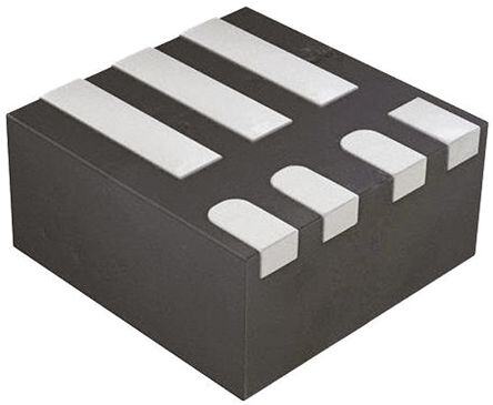
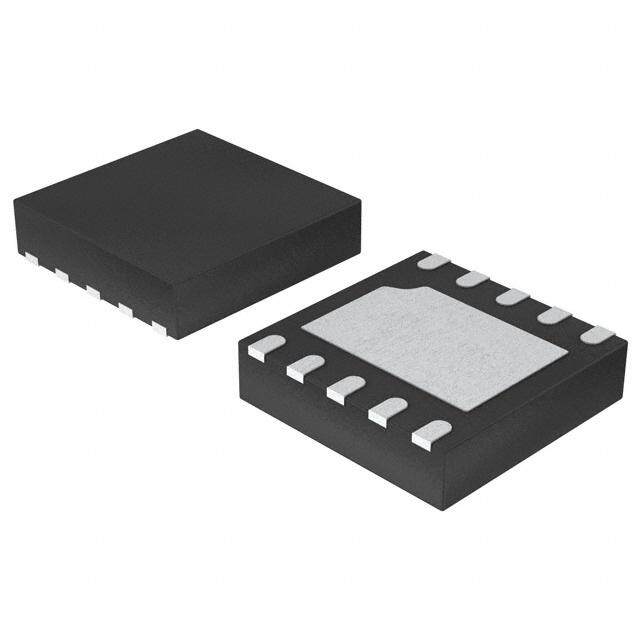
| 供应商器件封装 | 7-VQFN (2x2) |
| 关闭 | Shutdown |
| 其它名称 | 296-37085-1 |
| 制造商产品页 | http://www.ti.com/general/docs/suppproductinfo.tsp?distId=10&orderablePartNumber=TPS62085RLTT |
| 包装 | 剪切带 (CT) |
| 参考设计库 | http://designs.digikey.com/library/4294959904/4294959903/1340 |
| 同步整流器 | 是 |
| 商标 | Texas Instruments |
| 安装类型 | 表面贴装 |
| 安装风格 | SMD/SMT |
| 封装 | Reel |
| 封装/外壳 | 7-VFDFN |
| 封装/箱体 | VQFN-7 |
| 工作温度 | -40°C ~ 125°C |
| 工作温度范围 | - 40 C to + 85 C |
| 工厂包装数量 | 250 |
| 开关频率 | 2.4 MHz |
| 拓扑结构 | Buck |
| 最大工作温度 | + 85 C |
| 最大输入电压 | 6 V |
| 最小工作温度 | - 40 C |
| 最小输入电压 | 2.5 V |
| 标准包装 | 1 |
| 特色产品 | http://www.digikey.cn/product-highlights/zh/tps620858687-stepdown-converter/51349 |
| 电压-输入 | 2.5 V ~ 6 V |
| 电压-输出 | 0.8 V ~ 6 V |
| 电流-输出 | 3A |
| 电源电压-最小 | 2.5 V |
| 电源电流 | 17 uA |
| 类型 | Voltage Converter |
| 系列 | TPS62085 |
| 输出数 | 1 |
| 输出电压 | 800 mV to 6 V |
| 输出电流 | 3 A |
| 输出端数量 | 1 Output |
| 输出类型 | 可调式 |
| 频率-开关 | 2.4MHz |


- 商务部:美国ITC正式对集成电路等产品启动337调查
- 曝三星4nm工艺存在良率问题 高通将骁龙8 Gen1或转产台积电
- 太阳诱电将投资9.5亿元在常州建新厂生产MLCC 预计2023年完工
- 英特尔发布欧洲新工厂建设计划 深化IDM 2.0 战略
- 台积电先进制程称霸业界 有大客户加持明年业绩稳了
- 达到5530亿美元!SIA预计今年全球半导体销售额将创下新高
- 英特尔拟将自动驾驶子公司Mobileye上市 估值或超500亿美元
- 三星加码芯片和SET,合并消费电子和移动部门,撤换高东真等 CEO
- 三星电子宣布重大人事变动 还合并消费电子和移动部门
- 海关总署:前11个月进口集成电路产品价值2.52万亿元 增长14.8%


PDF Datasheet 数据手册内容提取
Product Order Technical Tools & Support & Folder Now Documents Software Community TPS62085,TPS62086,TPS62087 SLVSB70B–OCTOBER2013–REVISEDJULY2018 TPS6208x, 3-A Step-Down Converter With Hiccup Short-Circuit Protection In 2-mm × 2- mm VSON Package 1 Features 3 Description • DCS-Control™Topology The TPS62085, TPS62086, and TPS62087 devices 1 are high-frequency synchronous step-down • Upto95%Efficiency converters optimized for small solution size and high • HiccupShort-CircuitProtection efficiency. With an input voltage range of 2.5 V to • PowerSaveModeforLightLoadEfficiency 6.0 V, common battery technologies are supported. The devices focus on high-efficiency step-down • 100%DutyCycleforLowestDropout conversion over a wide output current range. At • 2.5-Vto6.0-VInputVoltageRange medium to heavy loads, the converter operates in • 17-μAOperatingQuiescentCurrent PWM mode and automatically enters Power Save Mode operation at light load to maintain high • 0.8-VtoV AdjustableOutputVoltage IN efficiencyovertheentireloadcurrentrange. • 1.8-Vand3.3-VFixedOutputVoltage To address the requirements of system power rails, • OutputDischarge the internal compensation circuit allows a large • PowerGoodOutput selection of external output capacitor values ranging • ThermalShutdownProtection from 10 µF to 150 µF. Together with its DCS-Control • Availablein2-mm ×2-mmVSONPackage architecture,excellentloadtransientperformanceand output voltage regulation accuracy are achieved. The • CreateaCustomDesignUsingthe: devices are available in a 2-mm × 2-mm VSON – TPS62085WEBENCH® PowerDesigner package. – TPS62086WEBENCH® PowerDesigner DeviceInformation(1) – TPS62087WEBENCH® PowerDesigner PARTNUMBER PACKAGE BODYSIZE(NOM) 2 Applications TPS62085 TPS62086 VSON(7) 2.00mm×2.00mm • Battery-PoweredApplications TPS62087 • Point-of-Load (1) For all available packages, see the orderable addendum at • ProcessorSupplies theendofthedatasheet. • HardDiskDrives 4 Typical Application Schematic TPS62087 L1 V 0.47µH V TypicalApplicationEfficiency IN VIN SW OUT 2.5V to 6V C1 C2 1.8V/3A 10µF EN VOS R3 22µF 100 1M FB 90 GND PG POWER GOOD ncy (%) 80 e Effici 70 Vin = 2.5V 60 Vin = 3.3V Vin = 4.2V Vout = 1.8 V Vin = 5.0V 50 0.001 0.010 0.100 1.000 Iout (A) C004 1 An IMPORTANT NOTICE at the end of this data sheet addresses availability, warranty, changes, use in safety-critical applications, intellectualpropertymattersandotherimportantdisclaimers.PRODUCTIONDATA.
TPS62085,TPS62086,TPS62087 SLVSB70B–OCTOBER2013–REVISEDJULY2018 www.ti.com Table of Contents 1 Features.................................................................. 1 9.4 DeviceFunctionalModes..........................................8 2 Applications........................................................... 1 10 ApplicationandImplementation.......................... 9 3 Description............................................................. 1 10.1 ApplicationInformation............................................9 4 TypicalApplicationSchematic............................. 1 10.2 TypicalApplication .................................................9 5 RevisionHistory..................................................... 2 11 PowerSupplyRecommendations..................... 15 6 DeviceOptions....................................................... 3 12 Layout................................................................... 15 12.1 LayoutGuidelines.................................................15 7 PinConfigurationandFunctions......................... 3 12.2 LayoutExample....................................................15 8 Specifications......................................................... 3 12.3 ThermalConsiderations........................................15 8.1 AbsoluteMaximumRatings......................................3 13 DeviceandDocumentationSupport................. 16 8.2 ESDRatings..............................................................4 13.1 DeviceSupport......................................................16 8.3 RecommendedOperatingConditions.......................4 13.2 DocumentationSupport........................................16 8.4 ThermalInformation..................................................4 13.3 RelatedLinks........................................................16 8.5 ElectricalCharacteristics...........................................4 13.4 CommunityResources..........................................16 8.6 TypicalCharacteristics..............................................5 13.5 Trademarks...........................................................17 9 DetailedDescription.............................................. 6 13.6 ElectrostaticDischargeCaution............................17 9.1 Overview...................................................................6 13.7 Glossary................................................................17 9.2 FunctionalBlockDiagram.........................................6 14 Mechanical,Packaging,andOrderable 9.3 FeatureDescription...................................................7 Information........................................................... 17 5 Revision History NOTE:Pagenumbersforpreviousrevisionsmaydifferfrompagenumbersinthecurrentversion. ChangesfromRevisionA(June2015)toRevisionB Page • ChangedpackagenamefromQFNtoVSONintheFeatureslist......................................................................................... 1 • AddedWebenchlinkstothedatasheet ................................................................................................................................ 1 • AddedSWnodeACvalueinAbsoluteMaximumRatingstable ........................................................................................... 3 • Changedf To:f inEquation1 ..................................................................................................................................... 7 PFM PSM • AddedFigure2toPowerSaveModesection........................................................................................................................ 7 • AddedTable1toPowerGoodsection ................................................................................................................................. 8 • ChangedMuratainductorpartnumberinTable5............................................................................................................... 11 ChangesfromOriginal(October2013)toRevisionA Page • AddedESDRatingstable,FeatureDescriptionsection,DeviceFunctionalModes,ApplicationandImplementation section,PowerSupplyRecommendationssection,Layoutsection,DeviceandDocumentationSupportsection,and Mechanical,Packaging,andOrderableInformationsection.................................................................................................. 1 2 SubmitDocumentationFeedback Copyright©2013–2018,TexasInstrumentsIncorporated ProductFolderLinks:TPS62085 TPS62086 TPS62087
TPS62085,TPS62086,TPS62087 www.ti.com SLVSB70B–OCTOBER2013–REVISEDJULY2018 6 Device Options PARTNUMBER(1) OUTPUTVOLTAGE TPS62085RLT Adjustable TPS62086RLT 3.3V TPS62087RLT 1.8V (1) Fordetailedorderinginformation,pleasechecktheMechanical,Packaging,andOrderableInformationsectionattheendofthis datasheet. 7 Pin Configuration and Functions RLTPackage 7-PinVSON TopView EN 1 7 VIN PG 2 6 SW FB 3 5 GND VOS 4 PinFunctions PIN I/O DESCRIPTION NAME NO. EN 1 IN Deviceenablepin.Toenablethedevice,thispinneedstobepulledhigh.Pullingthispinlowdisablesthe device.Thispinhasapulldownresistoroftypically400kΩwhenthedeviceisdisabled. FB 3 IN Feedbackpin.Forthefixedoutputvoltageversionsthispinmustbeconnectedtotheoutputvoltage. GND 5 Groundpin. PG 2 OUT Powergoodopendrainoutputpin.Thepullupresistorcannotbeconnectedtoanyvoltagehigherthan6V.If unused,leaveitfloating. SW 6 PWR Switchpinofthepowerstage. VIN 7 PWR Inputvoltagepin. VOS 4 IN Outputvoltagesensepin.Thispinmustbedirectlyconnectedtotheoutputcapacitor. 8 Specifications 8.1 Absolute Maximum Ratings overoperatingfree-airtemperaturerange(unlessotherwisenoted)(1) MIN MAX UNIT VIN,FB,VOS,EN,PG –0.3 7 VoltageatPins(2) SW(DC) –0.3 V +0.3 V IN SW(AC,lessthan100ns)(3) –3 11 OperatingJunction,T –40 150 °C J Temperature Storage,T –65 150 °C stg (1) StressesbeyondthoselistedunderAbsoluteMaximumRatingsmaycausepermanentdamagetothedevice.Thesearestressratings onlyandfunctionaloperationofthedeviceattheseoranyotherconditionsbeyondthoseindicatedunderRecommendedOperating Conditionsisnotimplied.Exposuretoabsolute–maximum–ratedconditionsforextendedperiodsmayaffectdevicereliability. (2) Allvoltagevaluesarewithrespecttonetworkgroundterminal. (3) Whileswitching. Copyright©2013–2018,TexasInstrumentsIncorporated SubmitDocumentationFeedback 3 ProductFolderLinks:TPS62085 TPS62086 TPS62087
TPS62085,TPS62086,TPS62087 SLVSB70B–OCTOBER2013–REVISEDJULY2018 www.ti.com 8.2 ESD Ratings VALUE UNIT Humanbodymodel(HBM),perANSI/ESDA/JEDECJS-001(1) ±2000 V(ESD) Electrostaticdischarge Chargeddevicemodel(CDM),perJEDECspecificationJESD22- ±500 V C101(2) (1) JEDECdocumentJEP155statesthat500-VHBMallowssafemanufacturingwithastandardESDcontrolprocess. (2) JEDECdocumentJEP157statesthat250-VCDMallowssafemanufacturingwithastandardESDcontrolprocess. 8.3 Recommended Operating Conditions(1) MIN NOM MAX UNIT V Inputvoltagerange 2.5 6 V IN I SinkcurrentatPGpin 1 mA SINK_PG V Pullupresistorvoltage 6 V PG T Operatingjunctiontemperature –40 125 °C J (1) RefertoApplicationandImplementationforfurtherinformation. 8.4 Thermal Information TPS6208x THERMALMETRIC(1) RLT[VSON] UNIT 7PINS R Junction-to-ambientthermalresistance 107.8 °C/W θJA R Junction-to-case(top)thermalresistance 66.2 °C/W θJC(top) R Junction-to-boardthermalresistance 17.1 °C/W θJB ψ Junction-to-topcharacterizationparameter 2.1 °C/W JT ψ Junction-to-boardcharacterizationparameter 17.1 °C/W JB R Junction-to-case(bottom)thermalresistance N/A °C/W θJC(bot) (1) Formoreinformationabouttraditionalandnewthermalmetrics,seetheSemiconductorandICPackageThermalMetricsapplication report(SPRA953). 8.5 Electrical Characteristics T =–40°Cto125°C,andV =3.6V.TypicalvaluesareatT =25°C,unlessotherwisenoted. J IN J PARAMETER TESTCONDITIONS MIN TYP MAX UNIT SUPPLY V Inputvoltagerange 2.5 6 V IN Noload,devicenotswitching I QuiescentcurrentintoVIN 17 25 µA Q T =–40°Cto85°C,V =2.5Vto5.5V J IN EN=Low, I ShutdowncurrentintoVIN 0.7 5 µA SD T =–40°Cto85°C,V =2.5Vto5.5V J IN Undervoltagelockoutthreshold V falling 2.1 2.2 2.3 V IN V UVLO Undervoltagelockouthysteresis V rising 200 mV IN Thermalshutdownthreshold T rising 150 °C J T JSD Thermalshutdownhysteresis T falling 20 °C J LOGICINTERFACEEN V High-levelinputvoltage V =2.5Vto6.0V 1.0 V IH IN V Low-levelinputvoltage V =2.5Vto6.0V 0.4 V IL IN I InputleakagecurrentintoENpin EN=High 0.01 0.16 µA EN,LKG R PulldownresistanceatENpin EN=Low 400 kΩ PD SOFTSTART,POWERGOOD t Soft-starttime TimefromENhighto95%ofV nominal 0.8 ms SS OUT V rising,referencedtoV nominal 93% 95% 98% OUT OUT V Powergoodthreshold PG V falling,referencedtoV nominal 88% 90% 93% OUT OUT 4 SubmitDocumentationFeedback Copyright©2013–2018,TexasInstrumentsIncorporated ProductFolderLinks:TPS62085 TPS62086 TPS62087
TPS62085,TPS62086,TPS62087 www.ti.com SLVSB70B–OCTOBER2013–REVISEDJULY2018 Electrical Characteristics (continued) T =–40°Cto125°C,andV =3.6V.TypicalvaluesareatT =25°C,unlessotherwisenoted. J IN J PARAMETER TESTCONDITIONS MIN TYP MAX UNIT V Low-leveloutputvoltage I =1mA 0.4 V PG,OL sink I InputleakagecurrentintoPGpin V =5.0V 0.01 0.16 µA PG,LKG PG OUTPUT Outputvoltagerange,TPS62085 0.8 V V IN VOUT Outputvoltageaccuracy, IOUT=1A,VIN≥VOUT+1V,PWMmode –1.0% 1.0% TPS62086,TPS62087(1) I =0A,V ≥V +1V,PSMmode –1.0% 2.1% OUT IN OUT I =1A,V ≥V +1V,PWMmode 792 800 808 V Feedbackregulationvoltage(1)(2) OUT IN OUT mV FB I =0A,V ≥V +1V,PSMmode 792 800 817 OUT IN OUT I Feedbackinputleakagecurrent V =1V 0.01 0.1 µA FB,LKG FB R Outputdischargeresistor EN=LOW,V =1.8V 260 Ω DIS OUT Lineregulation I =1A,V =2.5Vto6.0V 0.02 %/V OUT IN Loadregulation I =0.5Ato3A 0.16 %/A OUT POWERSWITCH High-sideFETON-resistance I =500mA 31 56 mΩ SW R DS(on) Low-sideFETON-resistance I =500mA 23 45 mΩ SW I High-sideFETswitchcurrentlimit 3.7 4.6 5.5 A LIM f PWMswitchingfrequency I =1A 2.4 MHz SW OUT (1) Formoreinformation,seePowerSaveMode. (2) Conditions:L=0.47μH,C =22μF OUT 8.6 Typical Characteristics 10M z) H 1M y ( c n e u eq 100k Fr g n hi c Swit 10k Vin = 2.5 V Vin = 3.6 V Vout = 1.2 V Vin = 6.0 V 1000 0.001 0.010 0.100 1.000 Iout (A) C007 Figure1. SwitchingFrequency Copyright©2013–2018,TexasInstrumentsIncorporated SubmitDocumentationFeedback 5 ProductFolderLinks:TPS62085 TPS62086 TPS62087
TPS62085,TPS62086,TPS62087 SLVSB70B–OCTOBER2013–REVISEDJULY2018 www.ti.com 9 Detailed Description 9.1 Overview The TPS62085, TPS62086, and TPS62087 synchronous step-down converters are based on the DCS-Control (Direct Control with Seamless transition into Power Save Mode) topology. This is an advanced regulation topologythatcombinestheadvantagesofhysteretic,voltage,andcurrentmodecontrolschemes. The DCS-Control topology operates in PWM (pulse width modulation) mode for medium to heavy load conditions and in Power Save Mode at light load currents. In PWM mode, the converter operates with its nominal switching frequency of 2.4 MHz, having a controlled frequency variation over the input voltage range. As the load current decreases, the converter enters Power Save Mode, reducing the switching frequency and minimizing the IC quiescent current to achieve high efficiency over the entire load current range. Because DCS-Control supports both operation modes (PWM and PSM) within a single building block, the transition from PWM mode to Power Save Mode is seamless and without effects on the output voltage. Fixed output voltage version provides smallest solution size combined with lowest no load current. The devices offer both excellent DC voltage and superior loadtransientregulation,combinedwithverylowoutputvoltageripple,minimizinginterferencewithRFcircuits. 9.2 Functional Block Diagram PG Hiccup V Counter VIN FB VREF High Side Current Sense Bandgap EN Undervoltage Lockout Thermal Shutdown 400 kΩ(2) MOSFETDriver SW Control Logic GND Ramp Direct Control Comparator and VOS Compensation Timer R1(1) ton FB ErrorAmplifier V REF R2(1) 260Ω DCS - ControlTM EN Output Discharge Logic Note: (1) R1, R2 are implemented in the fixed output voltage versions only. (2) When the device is enabled, the 400 kΩresistor is disconnected. 6 SubmitDocumentationFeedback Copyright©2013–2018,TexasInstrumentsIncorporated ProductFolderLinks:TPS62085 TPS62086 TPS62087
TPS62085,TPS62086,TPS62087 www.ti.com SLVSB70B–OCTOBER2013–REVISEDJULY2018 9.3 Feature Description 9.3.1 PowerSaveMode As the load current decreases, the TPS62085, TPS62086, and TPS62087 enter Power Save Mode (PSM) operation. During Power Save Mode, the converter operates with reduced switching frequency and with a minimum quiescent current maintaining high efficiency. The power save mode occurs when the inductor current becomes discontinuous. Power Save Mode is based on a fixed on-time architecture, as related in Equation 1. TheswitchingfrequencyoverthewholeloadcurrentrangeisalsoshowninFigure1foratypicalapplication. V OUT t =420ns´ ON V IN 2´I OUT f = PSM V V -V t 2 ´ IN ´ IN OUT ON V L OUT (1) In Power Save Mode, the output voltage rises slightly above the nominal output voltage, as shown in Figure 9. Thiseffectisminimizedbyincreasingtheoutputcapacitororinductorvalue.TheoutputvoltageaccuracyinPSM operationisreflectedintheelectricalspecificationtableandgivenfora22-μFoutputcapacitor. During PAUSE period in PSM (shown in Figure 2 ), the device does not change the PG pin state nor does it detect an UVLO event, in order to achieve a minimum quiescent current and maintain high efficiency at light loads. VOUT tPAUSE IINDUCTOR tON Figure2. PowerSaveModeWaveformDiagram 9.3.2 100%DutyCycleLowDropoutOperation The devices offer low input-to-output voltage difference by entering 100% duty cycle mode. In this mode, the high-side MOSFET switch is constantly turned on and the low-side MOSFET is switched off. This is particularly useful in battery powered applications to achieve the longest operation time by taking full advantage of the whole battery voltage range. The minimum input voltage to maintain output regulation, depending on the load current andoutputvoltagecanbecalculatedas: V = V +I ´(R +R ) IN,MIN OUT OUT,MAX DS(on) L with • V =Minimuminputvoltagetomaintainanoutputvoltage IN,MIN • I =Maximumoutputcurrent OUT,MAX • R =High-sideFETON-resistance DS(on) • R =Inductorohmicresistance(DCR) (2) L 9.3.3 SoftStart The TPS62085, TPS62086, and TPS62087 have an internal soft-start circuitry which monotonically ramps up the output voltage and reaches the nominal output voltage during a soft-start time of typically 0.8 ms. This avoids excessive inrush current and creates a smooth output voltage slope. It also prevents excessive voltage drops of primary cells and rechargeable batteries with high internal impedance. The device is able to start into a prebiased output capacitor. The device starts with the applied bias voltage and ramps the output voltage to its nominalvalue. Copyright©2013–2018,TexasInstrumentsIncorporated SubmitDocumentationFeedback 7 ProductFolderLinks:TPS62085 TPS62086 TPS62087
TPS62085,TPS62086,TPS62087 SLVSB70B–OCTOBER2013–REVISEDJULY2018 www.ti.com Feature Description (continued) 9.3.4 SwitchCurrentLimitandHiccupShort-CircuitProtection The switch current limit prevents the devices from high inductor current and from drawing excessive current from the battery or input voltage rail. Excessive current might occur with a shorted or saturated inductor or a heavy load or shorted output circuit condition. If the inductor current reaches the threshold I , the high-side MOSFET LIM is turned off and the low-side MOSFET is turned on to ramp down the inductor current. When this switch current limits is triggered 32 times, the devices stop switching and enable the output discharge. The devices then automatically start a new start-up after a typical delay time of 66 µs has passed. This is named HICCUP short- circuitprotection.Thedevicesrepeatthismodeuntilthehighloadconditiondisappears. 9.3.5 UndervoltageLockout To avoid misoperation of the device at low input voltages, an undervoltage lockout (UVLO) is implemented, whichshutsdownthedevicesatvoltageslowerthanV withahysteresisof200mV. UVLO 9.3.6 ThermalShutdown The device goes into thermal shutdown and stops switching when the junction temperature exceeds T . When JSD thedevicetemperaturefallsbelowthethresholdby20°C,thedevicereturnstonormaloperationautomatically. 9.4 Device Functional Modes 9.4.1 EnableandDisable The devices are enabled by setting the EN pin to a logic HIGH. Accordingly, shutdown mode is forced if the EN pinispulledLOWwithashutdowncurrentoftypically0.7μA. In shutdown mode, the internal power switches as well as the entire control circuitry are turned off. An internal resistor of 260 Ω discharges the output through the VOS pin smoothly. The output discharge function also works whenthermalshutdown,UVLO,orshort-circuitprotectionaretriggered. An internal pulldown resistor of 400 kΩ is connected to the EN pin when the EN pin is LOW. The pulldown resistorisdisconnectedwhentheENpinisHIGH. 9.4.2 PowerGood The TPS62085, TPS62086, and TPS62087 have a power good output. The power good goes high impedance once the output is above 95% of the nominal voltage, and is driven low once the output voltage falls below typically90%ofthenominalvoltage.ThePGpinisanopen-drainoutputandisspecifiedtosinkupto1mA.The power good output requires a pullup resistor connecting to any voltage rail less than 6 V. The PG signal can be used for sequencing of multiple rails by connecting it to the EN pin of other converters. Leave the PG pin unconnectedwhennotused.Table1showsthePGpinlogic. Table1.PGPinLogic LOGICSTATUS DEVICECONDITIONS HIGHZ LOW EN=High,V ≥V √ FB PG Enable EN=High,V <V √ FB PG Shutdown EN=Low √ ThermalShutdown T >T √ J JSD UVLO 0.5V<V <V √ IN UVLO PowerSupply V ≤0.5V √ Removal IN 8 SubmitDocumentationFeedback Copyright©2013–2018,TexasInstrumentsIncorporated ProductFolderLinks:TPS62085 TPS62086 TPS62087
TPS62085,TPS62086,TPS62087 www.ti.com SLVSB70B–OCTOBER2013–REVISEDJULY2018 10 Application and Implementation NOTE Information in the following applications sections is not part of the TI component specification, and TI does not warrant its accuracy or completeness. TI’s customers are responsible for determining suitability of components for their purposes. Customers should validateandtesttheirdesignimplementationtoconfirmsystemfunctionality. 10.1 Application Information The TPS62085 is a synchronous step-down converter in which output voltage is adjusted by component selection. The following section discusses the design of the external components to complete the power supply design for several input and output voltage options by using typical applications as a reference. The TPS62086 andTPS62087devicesprovideafixedoutputvoltagewhichdoesnotneedanexternalresistordivider. 10.2 Typical Application TPS62085 L1 0.47µH V V IN VIN SW OUT 2.5V to 6V C1 C2 1.2V/3A 10µF EN VOS R1 R3 22µF 80.6k 1M FB GND PG R2 162k POWER GOOD Figure3. 1.2-VOutputVoltageApplication 10.2.1 DesignRequirements Forthisdesignexample,usetheparameterslistedinTable2astheinputparameters. Table2.DesignParameters DESIGNPARAMETER EXAMPLEVALUE Inputvoltage 2.5Vto6V Outputvoltage 1.2V Outputripplevoltage <20mV Maximumoutputcurrent 3A Table3liststhecomponentsusedfortheexample. Table3.ListofComponents REFERENCE DESCRIPTION MANUFACTURER C1 10µF,Ceramiccapacitor,6.3V,X7R,size0805,GRM21BR71A106ME51L Murata C2 22µF,Ceramiccapacitor,6.3V,X5R,size0805,GRM21BR60J226ME39L Murata L1 0.47µH,PowerInductor,size4mm×4mm×1.5mm,XFL4015-471ME Coilcraft R1 Dependingontheoutputvoltage,1%,size0603;0ΩforTPS62086,TPS62087 Std R2 162kΩ,Chipresistor,1/16W,1%,size0603;openforTPS62086,TPS62087 Std R3 1MΩ,Chipresistor,1/16W,1%,size0603 Std 10.2.2 DetailedDesignProcedure 10.2.2.1 CustomDesignWithWEBENCH® Tools ClickheretocreateacustomdesignusingtheTPS62085devicewiththeWEBENCH® PowerDesigner. ClickheretocreateacustomdesignusingtheTPS62086devicewiththeWEBENCH® PowerDesigner. ClickheretocreateacustomdesignusingtheTPS62087devicewiththeWEBENCH® PowerDesigner. Copyright©2013–2018,TexasInstrumentsIncorporated SubmitDocumentationFeedback 9 ProductFolderLinks:TPS62085 TPS62086 TPS62087
TPS62085,TPS62086,TPS62087 SLVSB70B–OCTOBER2013–REVISEDJULY2018 www.ti.com 1. Startbyenteringtheinputvoltage(V ),outputvoltage(V ),andoutputcurrent(I )requirements. IN OUT OUT 2. Optimizethedesignforkeyparameterssuchasefficiency,footprint,andcostusingtheoptimizerdial. 3. ComparethegenerateddesignwithotherpossiblesolutionsfromTexasInstruments. The WEBENCH Power Designer provides a customized schematic along with a list of materials with real-time pricingandcomponentavailability. Inmostcases,theseactionsareavailable: • Runelectricalsimulationstoseeimportantwaveformsandcircuitperformance • Runthermalsimulationstounderstandboardthermalperformance • ExportcustomizedschematicandlayoutintopopularCADformats • PrintPDFreportsforthedesign,andsharethedesignwithcolleagues GetmoreinformationaboutWEBENCHtoolsatwww.ti.com/WEBENCH. 10.2.2.2 SettingTheOutputVoltage TheoutputvoltageissetbyanexternalresistordivideraccordingtoEquation3: æ R1ö æ R1ö V =V ´ 1+ =0.8V´ 1+ OUT FB çè R2÷ø çè R2÷ø (3) R2 must not be higher than 180 kΩ to achieve high efficiency at light load while providing acceptable noise sensitivity. Lowest operating quiescent current and best output voltage accuracy are achieved with the fixed outputvoltageversions.Forthefixedoutputvoltageversions,theFBpinmustbeconnectedtotheoutput. 10.2.2.3 OutputFilterDesign The inductor and the output capacitor together provide a low-pass filter. To simplify the selection process, Table4outlinespossibleinductorandcapacitorvaluecombinationsformostapplications. Table4.MatrixofOutputCapacitorandInductorCombinations NOMINALC [µF](2) NOMINALL[µH](1) OUT 10 22 47 100 150 0.47 +(3) + + + 1 + + + + + 2.2 (1) Inductortoleranceandcurrentderatingisanticipated.Theeffectiveinductancecanvaryby20%and –30%. (2) Capacitancetoleranceandbiasvoltagederatingisanticipated.Theeffectivecapacitancecanvaryby 20%and–50%. (3) Typicalapplicationconfiguration.Other'+'markindicatesrecommendedfiltercombinations. 10.2.2.4 InductorSelection The main parameter for the inductor selection is the inductor value and then the saturation current of the inductor.Tocalculatethemaximuminductorcurrentunderstaticloadconditions,Equation4 isgiven. DI I =I + L L,MAX OUT,MAX 2 V 1- OUT V DI = V ´ IN L OUT L´f SW where • I =Maximumoutputcurrent OUT,MAX • ΔI =Inductorcurrentripple L • f =Switchingfrequency SW • L=Inductorvalue (4) 10 SubmitDocumentationFeedback Copyright©2013–2018,TexasInstrumentsIncorporated ProductFolderLinks:TPS62085 TPS62086 TPS62087
TPS62085,TPS62086,TPS62087 www.ti.com SLVSB70B–OCTOBER2013–REVISEDJULY2018 TI recommends choosing the saturation current for the inductor 20% to 30% higher than the I , out of L,MAX Equation 4. A higher inductor value is also useful to lower ripple current but increases the transient response timeaswell.Thefollowinginductorsarerecommendedtobeusedindesigns. Table5.ListofRecommendedInductors INDUCTANCE CURRENTRATING DIMENSIONS DCRESISTANCE [µH] [A] L×W×H[mm3] [mΩtypical] PARTNUMBER 0.47 6.6 4×4×1.5 7.6 CoilcraftXFL4015-471 0.47 6.7 3.2×2.5×1.2 23 MurataDFE322512F-R47N 1 5.1 4×4×2 10.8 CoilcraftXFL4020-102 10.2.2.5 CapacitorSelection The input capacitor is the low-impedance energy source for the converters which helps to provide stable operation.AlowESRmultilayerceramiccapacitorisrecommendedforbestfilteringandmustbeplacedbetween VIN and GND as close as possible to those pins. For most applications, 10 μF is sufficient, though a larger value reducesinputcurrentripple. The architecture of the TPS62085, TPS62086, and TPS62087 allows the use of tiny ceramic output capacitors with low equivalent series resistance (ESR). These capacitors provide low output voltage ripple and are recommended. To keep its low resistance up to high frequencies and to get narrow capacitance variation with temperature, TI recommends using X7R or X5R dielectrics. The recommended typical output capacitor value is 22 μF; this capacitance can vary over a wide range as outline in the output filter selection table. Output capacitors above 150 µF may be used with a reduced load current during startup to avoid triggering the short circuitprotection. Afeed-forwardcapacitorisnotrequiredfordeviceproperoperation. 10.2.3 ApplicationCurves V =3.6V,V =1.2V,T =25ºC,unlessotherwisenoted IN OUT A Table6.TableofGraphs FIGURE TPS62085,V =0.95V Figure4 OUT TPS62085,V =1.2V Figure5 OUT Efficiency TPS62086,V =3.3V Figure6 OUT TPS62087,V =1.8V Figure7 OUT LineRegulation TPS62085 Figure8 LoadRegulation TPS62085 Figure9 SwitchingFrequency TPS62085 Figure1 TPS62085,PWMOperation(Load=3A) Figure10 TPS62085,PSMOperation(Load=100mA) Figure11 TPS62085,LoadSweep(Load=Opento3A) Figure12 TPS62085,Start-Up(Load=0.47Ω) Figure13 TPS62085,Start-Up(Load=Open) Figure14 TPS62085,Shutdown(Load=0.47Ω) Figure15 Waveforms TPS62085,Shutdown(Load=Open) Figure16 TPS62085,LoadTransient(Load=0.5Ato3A) Figure17 TPS62085,LoadTransient(Load=50mAto3A) Figure18 TPS62085,OutputShort-CircuitProtection(Load=0.47Ω,Entry) Figure19 TPS62085,OutputShort-CircuitProtection(Load=0.47Ω,Recovery) Figure20 TPS62085,OutputShort-CircuitProtection(Load=0.47Ω,HICCUPZoomIn) Figure21 Copyright©2013–2018,TexasInstrumentsIncorporated SubmitDocumentationFeedback 11 ProductFolderLinks:TPS62085 TPS62086 TPS62087
TPS62085,TPS62086,TPS62087 SLVSB70B–OCTOBER2013–REVISEDJULY2018 www.ti.com 100 100 90 90 ncy (%) 80 ncy (%) 80 e e Effici 70 Effici 70 Vin = 2.5 V Vin = 2.5 V 60 Vin = 3.3 V 60 Vin = 3.3 V Vin = 4.2 V Vin = 4.2 V Vout = 0.95 V Vin = 5.0 V Vout = 1.2 V Vin = 5.0 V 50 50 0.001 0.010 0.100 1.000 0.001 0.010 0.100 1.000 Iout (A) C001 Iout (A) C002 Figure4. Efficiency Figure5. Efficiency 100 100 90 90 ncy (%) 80 ncy (%) 80 e e Effici 70 Effici 70 Vin = 2.5V 60 Vin = 3.6 V 60 Vin = 3.3V Vin = 4.2 V Vin = 4.2V Vout = 3.3 V Vin = 5.0 V Vout = 1.8 V Vin = 5.0V 50 50 0.001 0.010 0.100 1.000 0.001 0.010 0.100 1.000 Iout (A) C003 Iout (A) C004 Figure6. Efficiency Figure7. Efficiency 1.212 1.212 1.206 1.206 V) V) ut (1.200 ut (1.200 o o V V 1.194 1.194 TA = -40 °C TA = -40 °C TA = 25 °C TA = 25 °C Vout = 1.2 V, Iout = 1 A TA = 85 °C Vout = 1.2 V, Vin = 3.6 V TA = 85 °C 1.188 1.188 2.5 3.0 3.5 4.0 4.5 5.0 5.5 6.0 0.001 0.010 0.100 1.000 Vin (V) C005 Iout (A) C006 Figure8. LineRegulation Figure9. LoadRegulation 12 SubmitDocumentationFeedback Copyright©2013–2018,TexasInstrumentsIncorporated ProductFolderLinks:TPS62085 TPS62086 TPS62087
TPS62085,TPS62086,TPS62087 www.ti.com SLVSB70B–OCTOBER2013–REVISEDJULY2018 t -- 300ns/div t -- 500ns/div Vout (AC, 20mV/div) Vout (AC, 20mV/div) Icoil (DC, 1A/div) Icoil (DC, 1A/div) SW (DC, 5V/div) SW (DC, 5V/div) Figure10. PWMOperation,Load=3A Figure11. PSMOperation,Load=100mA t -- 200μs/div t -- 200μs/div Load (DC, 2A/div) EN (DC, 5V/div) Vout (AC, 50mV/div) PG (DC, 5V/div) Vout (DC, 0.5V/div) Icoil (DC, 2A/div) Icoil (DC, 2A/div) Figure12. LoadSweep,Load=Opento3A Figure13. Start-Up,Load=0.47Ω t -- 200μs/div t -- 5μs/div EN (DC, 5V/div) EN (DC, 5V/div) Vout (DC, 0.5V/div) PG (DC, 5V/div) PG (DC, 5V/div) Vout (DC, 0.5V/div) Icoil (DC, 2A/div) Icoil (DC, 0.5A/div) Figure14. Start-Up,Load=Open Figure15. Shutdown,Load=0.47Ω Copyright©2013–2018,TexasInstrumentsIncorporated SubmitDocumentationFeedback 13 ProductFolderLinks:TPS62085 TPS62086 TPS62087
TPS62085,TPS62086,TPS62087 SLVSB70B–OCTOBER2013–REVISEDJULY2018 www.ti.com t -- 5ms/div t -- 2μs/div EN (DC, 5V/div) Load (DC, 2A/div) Vout (DC, 0.5V/div) PG (DC, 5V/div) PG (DC, 5V/div) Vout (DC, 0.1V/div) Icoil (DC, 0.5A/div) Icoil (DC, 2A/div) Figure16. Shutdown,Load=Open Figure17.LoadTransient,Load=0.5Ato3A t -- 3μs/div t -- 200μs/div Load (DC, 2A/div) PG (DC, 5V/div) Vout (DC, 0.5V/div) PG (DC, 5V/div) Vout (DC, 0.1V/div) Icoil (DC, 2A/div) Icoil (DC, 2A/div) Figure18. LoadTransient,Load=50mAto3A Figure19. OutputShort-CircuitProtection,Load=0.47Ω, Entry t -- 200μs/div t -- 5μs/div PG (DC, 5V/div) PG (DC, 5V/div) Vout (DC, 0.5V/div) Vout (DC, 0.5V/div) Icoil (DC, 2A/div) Icoil (DC, 2A/div) Figure20. OutputShort-CircuitProtection,Load=0.47Ω, Figure21.OutputShort-CircuitProtection,Load=0.47Ω, Recovery HICCUPZoomIn 14 SubmitDocumentationFeedback Copyright©2013–2018,TexasInstrumentsIncorporated ProductFolderLinks:TPS62085 TPS62086 TPS62087
TPS62085,TPS62086,TPS62087 www.ti.com SLVSB70B–OCTOBER2013–REVISEDJULY2018 11 Power Supply Recommendations The device is designed to operate from an input voltage supply range from 2.5 V to 6 V. Ensure that the input powersupplyhasasufficientcurrentratingfortheapplication. 12 Layout 12.1 Layout Guidelines The printed-circuit-board (PCB) layout is an important step to maintain the high performance of the TPS62085, TPS62086,andTPS62087devices. The input and output capacitors and the inductor must be placed as close as possible to the IC. This keeps the traces short. Routing these traces direct and wide results in low trace resistance and low parasitic inductance. The low side of the input and output capacitors must be connected directly to the GND pin to avoid a ground potential shift. The sense traces connected to FB and VOS pins are signal traces. Special care must be taken to avoidnoisebeinginduced.Byadirectrouting,parasiticinductancecanbekeptsmall.GNDlayersmightbeused forshielding.KeepthesetracesawayfromSWnodes.SeeFigure22 fortherecommendedPCBlayout. 12.2 Layout Example L1 VOUT VIN C1 C2 Solution Size 62 mm2 VIN SW GND GND ENPGFBVOS R2 R1 Figure22. PCBLayoutRecommendation 12.3 Thermal Considerations Implementation of integrated circuits in low-profile and fine-pitch surface-mount packages typically requires special attention to power dissipation. Many system-dependent issues such as thermal coupling, airflow, added heat sinks and convection surfaces, and the presence of other heat-generating components affect the power dissipationlimitsofagivencomponent. Twobasicapproachesforenhancingthermalperformanceare: • ImprovingthepowerdissipationcapabilityofthePCBdesign • Introducingairflowinthesystem The Thermal Data section in the TPS62085EVM-169 Evaluation Module User's Guide (SLVU809) provides the thermal metric of the device on the EVM after considering the PCB design of real applications. The big copper planes connecting to the pads of the IC on the PCB improve the thermal performance of the device. For more details on how to use the thermal parameters, see the Thermal Characteristics Application Notes, SZZA017 and SPRA953. Copyright©2013–2018,TexasInstrumentsIncorporated SubmitDocumentationFeedback 15 ProductFolderLinks:TPS62085 TPS62086 TPS62087
TPS62085,TPS62086,TPS62087 SLVSB70B–OCTOBER2013–REVISEDJULY2018 www.ti.com 13 Device and Documentation Support 13.1 Device Support 13.1.1 Third-PartyProductsDisclaimer TI'S PUBLICATION OF INFORMATION REGARDING THIRD-PARTY PRODUCTS OR SERVICES DOES NOT CONSTITUTE AN ENDORSEMENT REGARDING THE SUITABILITY OF SUCH PRODUCTS OR SERVICES OR A WARRANTY, REPRESENTATION OR ENDORSEMENT OF SUCH PRODUCTS OR SERVICES, EITHER ALONEORINCOMBINATIONWITHANYTIPRODUCTORSERVICE. 13.1.2 CustomDesignWithWEBENCH® Tools ClickheretocreateacustomdesignusingtheTPS62085devicewiththeWEBENCH® PowerDesigner. ClickheretocreateacustomdesignusingtheTPS62086devicewiththeWEBENCH® PowerDesigner. ClickheretocreateacustomdesignusingtheTPS62087devicewiththeWEBENCH® PowerDesigner. 1. Startbyenteringtheinputvoltage(V ),outputvoltage(V ),andoutputcurrent(I )requirements. IN OUT OUT 2. Optimizethedesignforkeyparameterssuchasefficiency,footprint,andcostusingtheoptimizerdial. 3. ComparethegenerateddesignwithotherpossiblesolutionsfromTexasInstruments. The WEBENCH Power Designer provides a customized schematic along with a list of materials with real-time pricingandcomponentavailability. Inmostcases,theseactionsareavailable: • Runelectricalsimulationstoseeimportantwaveformsandcircuitperformance • Runthermalsimulationstounderstandboardthermalperformance • ExportcustomizedschematicandlayoutintopopularCADformats • PrintPDFreportsforthedesign,andsharethedesignwithcolleagues GetmoreinformationaboutWEBENCHtoolsatwww.ti.com/WEBENCH. 13.2 Documentation Support 13.2.1 RelatedDocumentation Forrelateddocumentation,seethefollowing: • TPS62085EVM-169EvaluationModuleUser'sGuide,SLVU809 • ThermalCharacteristicsApplicationNote,SZZA017 • ThermalCharacteristicsApplicationNote,SPRA953 13.3 Related Links The table below lists quick access links. Categories include technical documents, support and community resources,toolsandsoftware,andquickaccesstosampleorbuy. Table7.RelatedLinks TECHNICAL TOOLS& SUPPORT& PARTS PRODUCTFOLDER SAMPLE&BUY DOCUMENTS SOFTWARE COMMUNITY TPS62085 Clickhere Clickhere Clickhere Clickhere Clickhere TPS62086 Clickhere Clickhere Clickhere Clickhere Clickhere TPS62087 Clickhere Clickhere Clickhere Clickhere Clickhere 13.4 Community Resources The following links connect to TI community resources. Linked contents are provided "AS IS" by the respective contributors. They do not constitute TI specifications and do not necessarily reflect TI's views; see TI's Terms of Use. TIE2E™OnlineCommunity TI'sEngineer-to-Engineer(E2E)Community.Createdtofostercollaboration 16 SubmitDocumentationFeedback Copyright©2013–2018,TexasInstrumentsIncorporated ProductFolderLinks:TPS62085 TPS62086 TPS62087
TPS62085,TPS62086,TPS62087 www.ti.com SLVSB70B–OCTOBER2013–REVISEDJULY2018 Community Resources (continued) amongengineers.Ate2e.ti.com,youcanaskquestions,shareknowledge,exploreideasandhelp solveproblemswithfellowengineers. DesignSupport TI'sDesignSupport QuicklyfindhelpfulE2Eforumsalongwithdesignsupporttoolsand contactinformationfortechnicalsupport. 13.5 Trademarks DCS-Control,E2EaretrademarksofTexasInstruments. WEBENCHisaregisteredtrademarkofTexasInstruments. 13.6 Electrostatic Discharge Caution Thesedeviceshavelimitedbuilt-inESDprotection.Theleadsshouldbeshortedtogetherorthedeviceplacedinconductivefoam duringstorageorhandlingtopreventelectrostaticdamagetotheMOSgates. 13.7 Glossary SLYZ022—TIGlossary. Thisglossarylistsandexplainsterms,acronyms,anddefinitions. 14 Mechanical, Packaging, and Orderable Information The following pages include mechanical, packaging, and orderable information. This information is the most current data available for the designated devices. This data is subject to change without notice and revision of thisdocument.Forbrowser-basedversionsofthisdatasheet,refertotheleft-handnavigation. Copyright©2013–2018,TexasInstrumentsIncorporated SubmitDocumentationFeedback 17 ProductFolderLinks:TPS62085 TPS62086 TPS62087
PACKAGE OPTION ADDENDUM www.ti.com 10-Jul-2020 PACKAGING INFORMATION Orderable Device Status Package Type Package Pins Package Eco Plan Lead finish/ MSL Peak Temp Op Temp (°C) Device Marking Samples (1) Drawing Qty (2) Ball material (3) (4/5) (6) TPS62085RLTR ACTIVE VSON-HR RLT 7 3000 Green (RoHS Call TI | NIPDAU Level-1-260C-UNLIM -40 to 125 PD5Q & no Sb/Br) TPS62085RLTT ACTIVE VSON-HR RLT 7 250 Green (RoHS Call TI | NIPDAU Level-1-260C-UNLIM -40 to 125 PD5Q & no Sb/Br) TPS62086RLTR ACTIVE VSON-HR RLT 7 3000 Green (RoHS NIPDAU Level-1-260C-UNLIM -40 to 125 PD4Q & no Sb/Br) TPS62086RLTT ACTIVE VSON-HR RLT 7 250 Green (RoHS NIPDAU Level-1-260C-UNLIM -40 to 125 PD4Q & no Sb/Br) TPS62087RLTR ACTIVE VSON-HR RLT 7 3000 Green (RoHS NIPDAU Level-1-260C-UNLIM -40 to 125 PD3Q & no Sb/Br) TPS62087RLTT ACTIVE VSON-HR RLT 7 250 Green (RoHS NIPDAU Level-1-260C-UNLIM -40 to 125 PD3Q & no Sb/Br) (1) The marketing status values are defined as follows: ACTIVE: Product device recommended for new designs. LIFEBUY: TI has announced that the device will be discontinued, and a lifetime-buy period is in effect. NRND: Not recommended for new designs. Device is in production to support existing customers, but TI does not recommend using this part in a new design. PREVIEW: Device has been announced but is not in production. Samples may or may not be available. OBSOLETE: TI has discontinued the production of the device. (2) RoHS: TI defines "RoHS" to mean semiconductor products that are compliant with the current EU RoHS requirements for all 10 RoHS substances, including the requirement that RoHS substance do not exceed 0.1% by weight in homogeneous materials. Where designed to be soldered at high temperatures, "RoHS" products are suitable for use in specified lead-free processes. TI may reference these types of products as "Pb-Free". RoHS Exempt: TI defines "RoHS Exempt" to mean products that contain lead but are compliant with EU RoHS pursuant to a specific EU RoHS exemption. Green: TI defines "Green" to mean the content of Chlorine (Cl) and Bromine (Br) based flame retardants meet JS709B low halogen requirements of <=1000ppm threshold. Antimony trioxide based flame retardants must also meet the <=1000ppm threshold requirement. (3) MSL, Peak Temp. - The Moisture Sensitivity Level rating according to the JEDEC industry standard classifications, and peak solder temperature. (4) There may be additional marking, which relates to the logo, the lot trace code information, or the environmental category on the device. (5) Multiple Device Markings will be inside parentheses. Only one Device Marking contained in parentheses and separated by a "~" will appear on a device. If a line is indented then it is a continuation of the previous line and the two combined represent the entire Device Marking for that device. Addendum-Page 1
PACKAGE OPTION ADDENDUM www.ti.com 10-Jul-2020 (6) Lead finish/Ball material - Orderable Devices may have multiple material finish options. Finish options are separated by a vertical ruled line. Lead finish/Ball material values may wrap to two lines if the finish value exceeds the maximum column width. Important Information and Disclaimer:The information provided on this page represents TI's knowledge and belief as of the date that it is provided. TI bases its knowledge and belief on information provided by third parties, and makes no representation or warranty as to the accuracy of such information. Efforts are underway to better integrate information from third parties. TI has taken and continues to take reasonable steps to provide representative and accurate information but may not have conducted destructive testing or chemical analysis on incoming materials and chemicals. TI and TI suppliers consider certain information to be proprietary, and thus CAS numbers and other limited information may not be available for release. In no event shall TI's liability arising out of such information exceed the total purchase price of the TI part(s) at issue in this document sold by TI to Customer on an annual basis. Addendum-Page 2
PACKAGE MATERIALS INFORMATION www.ti.com 20-Jul-2019 TAPE AND REEL INFORMATION *Alldimensionsarenominal Device Package Package Pins SPQ Reel Reel A0 B0 K0 P1 W Pin1 Type Drawing Diameter Width (mm) (mm) (mm) (mm) (mm) Quadrant (mm) W1(mm) TPS62085RLTR VSON- RLT 7 3000 180.0 8.4 2.3 2.3 1.15 4.0 8.0 Q2 HR TPS62085RLTT VSON- RLT 7 250 180.0 8.4 2.3 2.3 1.15 4.0 8.0 Q2 HR TPS62086RLTR VSON- RLT 7 3000 180.0 8.4 2.3 2.3 1.15 4.0 8.0 Q2 HR TPS62086RLTT VSON- RLT 7 250 180.0 8.4 2.3 2.3 1.15 4.0 8.0 Q2 HR TPS62086RLTT VSON- RLT 7 250 179.0 8.4 2.2 2.2 1.2 4.0 8.0 Q2 HR TPS62087RLTR VSON- RLT 7 3000 180.0 8.4 2.3 2.3 1.15 4.0 8.0 Q2 HR TPS62087RLTT VSON- RLT 7 250 180.0 8.4 2.3 2.3 1.15 4.0 8.0 Q2 HR PackMaterials-Page1
PACKAGE MATERIALS INFORMATION www.ti.com 20-Jul-2019 *Alldimensionsarenominal Device PackageType PackageDrawing Pins SPQ Length(mm) Width(mm) Height(mm) TPS62085RLTR VSON-HR RLT 7 3000 182.0 182.0 20.0 TPS62085RLTT VSON-HR RLT 7 250 182.0 182.0 20.0 TPS62086RLTR VSON-HR RLT 7 3000 182.0 182.0 20.0 TPS62086RLTT VSON-HR RLT 7 250 182.0 182.0 20.0 TPS62086RLTT VSON-HR RLT 7 250 203.0 203.0 35.0 TPS62087RLTR VSON-HR RLT 7 3000 182.0 182.0 20.0 TPS62087RLTT VSON-HR RLT 7 250 182.0 182.0 20.0 PackMaterials-Page2
PACKAGE OUTLINE RLT0007A VSON - 1 mm max height PLASTIC SMALL OUTLINE - NO LEAD 2.1 A B 1.9 1 PIN 1 INDEX AREA 2.1 1.9 C 1 MAX SEATING PLANE 0.08 0.05 0.00 0.5 3X (0.2) TYP 0.3 (0.2) TYP 3X 0.5 4 2X 0.6 5 1.2 1.5 7 1 4X 00..32 1.4 3X 00..3255 3X 0.1 C A B 1.2 0.1 C A B 0.05 C PIN 1 ID 0.05 C 0.5 0.3 4220429/A 09/2014 NOTES: 1. All linear dimensions are in millimeters. Any dimensions in parenthesis are for reference only. Dimensioning and tolerancing per ASME Y14.5M. 2. This drawing is subject to change without notice. www.ti.com
EXAMPLE BOARD LAYOUT RLT0007A VSON - 1 mm max height PLASTIC SMALL OUTLINE - NO LEAD PKG (0.6) ℄ 1 (0.25) 7 2X (0.6) PKG 3X (0.5) ℄ 3X (0.25) 5 3X (0.3) 4 3X (1.5) 3X (0.6) (0.9) (0.45) LAND PATTERN EXAMPLE SCALE: 30X 0.07 MAX 0.07 MIN ALL AROUND ALL AROUND SOLDER MASK METAL OPENING SOLDER MASK METAL UNDER OPENING SOLDER MASK NON SOLDER MASK SOLDER MASK DEFINED DEFINED PADS 1 - 4 PADS 5 - 7 SOLDER MASK DETAILS 4220429/A 09/2014 NOTES: (continued) 3. For more information, see Texas Instruments literature number SLUA271 (www.ti.com/lit/slua271). 4. Solder mask tolerances between and around signal pads can vary based on board fabrication site. 5. Vias should not be placed on soldering pads unless they are plugged or plated shut. www.ti.com
EXAMPLE STENCIL DESIGN RLT0007A VSON - 1 mm max height PLASTIC SMALL OUTLINE - NO LEAD (0.6) PKG 6X (0.65) (0.21) ℄ 1 7 EXPOSED METAL TYP 2X (0.6) PKG 3X (0.5) ℄ METAL UNDER SOLDER MASK TYP 3X (0.21) 6X (0.3) 4 5 3X (0.025) 3X 3X (0.6) EXPOSED METAL (0.9) (0.875) SOLDER MASK EDGE TYP SOLDER PASTE EXAMPLE BASED ON 0.125 mm THICK STENCIL FOR ALL EXPOSED PADS 85% PRINTED SOLDER COVERAGE BY AREA SCALE: 40X 4220429/A 09/2014 NOTES: (continued) 6. Laser cutting apertures with trapezoidal walls and rounded corners may offer better paste release. IPC-7525 may have alternate design recommendations. www.ti.com
IMPORTANTNOTICEANDDISCLAIMER TI PROVIDES TECHNICAL AND RELIABILITY DATA (INCLUDING DATASHEETS), DESIGN RESOURCES (INCLUDING REFERENCE DESIGNS), APPLICATION OR OTHER DESIGN ADVICE, WEB TOOLS, SAFETY INFORMATION, AND OTHER RESOURCES “AS IS” AND WITH ALL FAULTS, AND DISCLAIMS ALL WARRANTIES, EXPRESS AND IMPLIED, INCLUDING WITHOUT LIMITATION ANY IMPLIED WARRANTIES OF MERCHANTABILITY, FITNESS FOR A PARTICULAR PURPOSE OR NON-INFRINGEMENT OF THIRD PARTY INTELLECTUAL PROPERTY RIGHTS. These resources are intended for skilled developers designing with TI products. You are solely responsible for (1) selecting the appropriate TI products for your application, (2) designing, validating and testing your application, and (3) ensuring your application meets applicable standards, and any other safety, security, or other requirements. These resources are subject to change without notice. TI grants you permission to use these resources only for development of an application that uses the TI products described in the resource. Other reproduction and display of these resources is prohibited. No license is granted to any other TI intellectual property right or to any third party intellectual property right. TI disclaims responsibility for, and you will fully indemnify TI and its representatives against, any claims, damages, costs, losses, and liabilities arising out of your use of these resources. TI’s products are provided subject to TI’s Terms of Sale (www.ti.com/legal/termsofsale.html) or other applicable terms available either on ti.com or provided in conjunction with such TI products. TI’s provision of these resources does not expand or otherwise alter TI’s applicable warranties or warranty disclaimers for TI products. Mailing Address: Texas Instruments, Post Office Box 655303, Dallas, Texas 75265 Copyright © 2020, Texas Instruments Incorporated