ICGOO在线商城 > 集成电路(IC) > PMIC - 稳压器 - DC DC 开关稳压器 > LM2841YQMK/NOPB

 Datasheet下载
- 型号: LM2841YQMK/NOPB
- 制造商: Texas Instruments
- 库位|库存: xxxx|xxxx
- 要求:
| 数量阶梯 | 香港交货 | 国内含税 |
| +xxxx | $xxxx | ¥xxxx |
查看当月历史价格
查看今年历史价格
LM2841YQMK/NOPB产品简介:
ICGOO电子元器件商城为您提供LM2841YQMK/NOPB由Texas Instruments设计生产,在icgoo商城现货销售,并且可以通过原厂、代理商等渠道进行代购。 LM2841YQMK/NOPB价格参考。Texas InstrumentsLM2841YQMK/NOPB封装/规格:PMIC - 稳压器 - DC DC 开关稳压器, 可调式 降压 开关稳压器 IC 正 0.765V 1 输出 300mA SOT-23-6 细型,TSOT-23-6。您可以下载LM2841YQMK/NOPB参考资料、Datasheet数据手册功能说明书,资料中有LM2841YQMK/NOPB 详细功能的应用电路图电压和使用方法及教程。
LM2841YQMK/NOPB 是由德州仪器(Texas Instruments)生产的一款 PMIC - DC/DC 开关稳压器。它是一款高效、同步降压转换器,适用于多种需要高效率和低功耗的应用场景。以下是该型号的一些典型应用场景:

 1. 便携式电子设备
   - LM2841YQMK/NOPB 的高效能特性使其非常适合用于便携式设备,例如智能手机、平板电脑、笔记本电脑和其他电池供电的电子产品。它可以将较高的输入电压(如锂离子电池的电压)转换为稳定的较低输出电压,以满足设备中各种组件的供电需求。

 2. 通信设备
   - 在无线通信模块、路由器、调制解调器等设备中,该芯片可以为射频(RF)电路、基带处理器和其他关键组件提供稳定的电源。其高效的转换能力有助于降低热量产生,从而提高设备的可靠性和使用寿命。

 3. 工业自动化
   - 在工业控制领域,例如可编程逻辑控制器(PLC)、数据采集系统(DAQ)和传感器接口中,LM2841YQMK/NOPB 可以为微控制器、数字信号处理器(DSP)以及其他低功耗组件提供稳定的电源支持。其宽输入电压范围和高效率特性使其能够适应复杂的工业环境。

 4. 汽车电子
   - 该芯片可以在汽车电子系统中使用,例如车载信息娱乐系统、导航设备和高级驾驶辅助系统(ADAS)。它能够承受汽车环境中常见的电压波动,并为敏感的电子组件提供稳定的电源。

 5. 消费类电子产品
   - 在数码相机、游戏机、智能音箱等消费类电子产品中,LM2841YQMK/NOPB 可以提供高效的电源管理解决方案。它的紧凑设计和低功耗特性有助于实现更小、更轻的产品设计。

 6. 医疗设备
   - 在便携式医疗设备(如血糖仪、脉搏血氧仪等)中,该芯片可以为传感器、显示屏和处理器提供稳定且高效的电源。其低噪声特性也有助于提高设备的测量精度。

 核心优势:
- 高效率:在宽负载范围内保持高效率,延长电池寿命。
- 低静态电流:适合电池供电应用,减少待机功耗。
- 宽输入电压范围:支持多种电源输入场景。
- 小型封装:便于集成到空间受限的设计中。

综上所述,LM2841YQMK/NOPB 凭借其高效、可靠和灵活的特点,广泛应用于便携式设备、通信系统、工业自动化、汽车电子、消费类电子产品以及医疗设备等领域。
| 参数 | 数值 |
| 产品目录 | 集成电路 (IC)半导体 |
| 描述 | IC REG BUCK ADJ 0.3A TSOT23-6稳压器—开关式稳压器 300 mA up to 42V Input Step-Down DC/DC Regulator in Thin SOT-23 6-SOT -40 to 125 |
| 产品分类 | |
| 品牌 | Texas Instruments |
| 产品手册 | http://www.ti.com/lit/gpn/lm2841-q1 |
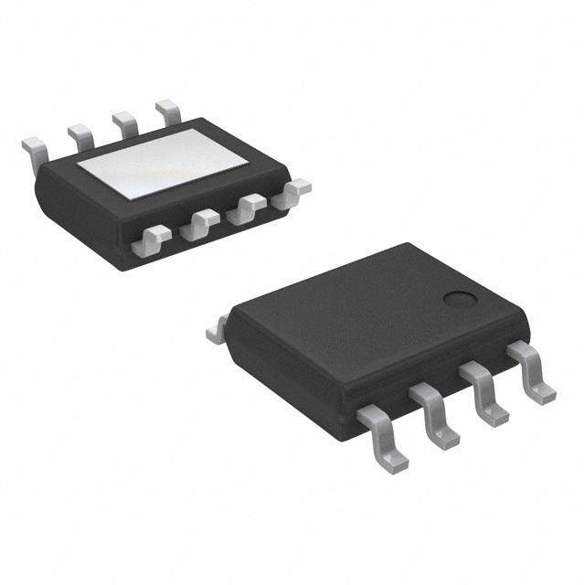
| 产品图片 |
|
| rohs | 符合RoHS无铅 / 符合限制有害物质指令(RoHS)规范要求 |
| 产品系列 | 电源管理 IC,稳压器—开关式稳压器,Texas Instruments LM2841YQMK/NOPB- |
| 数据手册 | |
| 产品型号 | LM2841YQMK/NOPB |
| PWM类型 | 电流模式 |
| 产品种类 | 稳压器—开关式稳压器 |
| 供应商器件封装 | TSOT-23-6 |
| 其它名称 | *LM2841YQMK/NOPB |
| 包装 | 剪切带 (CT) |
| 同步整流器 | 无 |
| 商标 | Texas Instruments |
| 安装类型 | 表面贴装 |
| 安装风格 | SMD/SMT |
| 封装 | Reel |
| 封装/外壳 | SOT-23-6 细型,TSOT-23-6 |
| 封装/箱体 | SOT-23-6 |
| 工作温度 | -40°C ~ 125°C |
| 工作温度范围 | - 40 C to + 125 C |
| 工厂包装数量 | 1000 |
| 开关频率 | 1.25 MHz |
| 最大输入电压 | 42 V |
| 标准包装 | 1 |
| 电压-输入 | 4.5 V ~ 42 V |
| 电压-输出 | 0.765 V ~ 34 V |
| 电流-输出 | 300mA |
| 类型 | Voltage Converter |
| 系列 | LM2841-Q1 |
| 输出数 | 1 |
| 输出电压 | 765 mV to 34 V |
| 输出电流 | 300 mA |
| 输出类型 | 可调式 |
| 配用 | /product-detail/zh/LM2841YMK-ADJEV%2FNOPB/LM2841YMK-ADJEV%2FNOPB-ND/2506740 |
| 频率-开关 | 1.25MHz |


- 商务部:美国ITC正式对集成电路等产品启动337调查
- 曝三星4nm工艺存在良率问题 高通将骁龙8 Gen1或转产台积电
- 太阳诱电将投资9.5亿元在常州建新厂生产MLCC 预计2023年完工
- 英特尔发布欧洲新工厂建设计划 深化IDM 2.0 战略
- 台积电先进制程称霸业界 有大客户加持明年业绩稳了
- 达到5530亿美元!SIA预计今年全球半导体销售额将创下新高
- 英特尔拟将自动驾驶子公司Mobileye上市 估值或超500亿美元
- 三星加码芯片和SET,合并消费电子和移动部门,撤换高东真等 CEO
- 三星电子宣布重大人事变动 还合并消费电子和移动部门
- 海关总署:前11个月进口集成电路产品价值2.52万亿元 增长14.8%


PDF Datasheet 数据手册内容提取
Product Order Technical Tools & Support & Folder Now Documents Software Community LM2840,LM2841,LM2842 SNVS540K–MARCH2009–REVISEDAPRIL2019 ® LM284x SIMPLE SWITCHER 4.5-V to 42-V Input, 0.1-, 0.3-, or 0.6-A Output Step-Down DC/DC Regulator in Thin SOT 1 Features 3 Description • Inputvoltage4.5Vto42V The LM284x SIMPLE SWITCHER™ devices are 1 PWM DC/DC buck (step-down) regulators. With an • Outputcurrentoptionsof100mA,300mA,and input range from 4.5 V to 42 V, they are suitable for a 600mA wide range of applications, such as power • Feedbackpinvoltageof0.765V conditioning from unregulated sources. They feature • 550-kHz(X)or1.25-MHz(Y)switchingfrequency a low RDSON (0.9‑Ω typical) internal switch for maximum efficiency (85% typical). Operating • LowshutdownI :16-µAtypical Q frequency is fixed at 550 kHz (X option) and • Short-circuitprotected 1.25 MHz (Y option), allowing the use of small • Internallycompensated externalcomponentswhilestillbeingable to have low output voltage ripple. Soft start can be implemented • Soft-startcircuitry using the shutdown (SHDN) pin with an external RC • Smalloverallsolutionsize(SOT-6Lpackage) circuit allowing the user to tailor the soft-start time to • CreateacustomdesignusingtheLM2840(or aspecificapplication. LM2841/42)withtheWEBENCH®PowerDesigner The LM2840 is optimized for up to 100 mA, the LM2841 for up to 300 mA, and the LM2842 for up to 2 Applications 600‑mA load currents. They all have a 0.765-V • Battery-poweredequipment nominalfeedbackvoltage. • Industrialdistributedpowerapplications Additional features include: thermal shutdown, V IN • Portablemediaplayers undervoltage lockout, and gate-drive undervoltage lockout. The LM284x are available in a low-profile • Portablehand-heldinstruments SOT-6Lpackage. DeviceInformation(1) PARTNUMBER PACKAGE BODYSIZE(NOM) LM2840,LM2841, SOT(6) 1.60mm×2.90mm LM2842 (1) For all available packages, see the orderable addendum at theendofthedatasheet. TypicalApplicationCircuit C BOOT L1 VOUT LM2840/1/2-ADJL VIN VIN CB D1 SHDN SW GND FB R1 CIN R2 COUT Copyright © 2016, Texas Instruments Incorporated 1 An IMPORTANT NOTICE at the end of this data sheet addresses availability, warranty, changes, use in safety-critical applications, intellectualpropertymattersandotherimportantdisclaimers.PRODUCTIONDATA.
LM2840,LM2841,LM2842 SNVS540K–MARCH2009–REVISEDAPRIL2019 www.ti.com Table of Contents 1 Features.................................................................. 1 8 ApplicationandImplementation........................ 11 2 Applications........................................................... 1 8.1 ApplicationInformation............................................11 3 Description............................................................. 1 8.2 TypicalApplications................................................11 4 RevisionHistory..................................................... 2 9 PowerSupplyRecommendations...................... 16 5 PinConfigurationandFunctions......................... 3 10 Layout................................................................... 16 6 Specifications......................................................... 4 10.1 LayoutGuidelines.................................................16 6.1 AbsoluteMaximumRatings .....................................4 10.2 LayoutExample....................................................16 6.2 ESDRatings..............................................................4 11 DeviceandDocumentationSupport................. 17 6.3 RecommendedOperatingConditions.......................4 11.1 DeviceSupport......................................................17 6.4 ThermalInformation..................................................4 11.2 DocumentationSupport........................................17 6.5 ElectricalCharacteristics..........................................5 11.3 RelatedLinks........................................................17 6.6 TypicalCharacteristics..............................................7 11.4 ReceivingNotificationofDocumentationUpdates17 7 DetailedDescription.............................................. 9 11.5 CommunityResources..........................................18 7.1 Overview...................................................................9 11.6 Trademarks...........................................................18 7.2 FunctionalBlockDiagram.........................................9 11.7 ElectrostaticDischargeCaution............................18 7.3 FeatureDescription...................................................9 11.8 Glossary................................................................18 7.4 DeviceFunctionalModes........................................10 12 Mechanical,Packaging,andOrderable Information........................................................... 18 4 Revision History NOTE:Pagenumbersforpreviousrevisionsmaydifferfrompagenumbersinthecurrentversion. ChangesfromRevisionJ(February2017)toRevisionK Page • Splitautomotivedatasheettoseparatedocument(SNVSBE5)andremoveautomotive-specificcontentfromSNVS540..1 • AddedSIMPLESWITCHER®todatasheettitle ................................................................................................................... 1 ChangesfromRevisionI(September2016)toRevisionJ Page • AddednewtextforPin4........................................................................................................................................................ 3 • AddedthisnewlineoftextinShutdownOperationsection................................................................................................. 13 ChangesfromRevisionH(April2013)toRevisionI Page • AddedESDRatingstable,FeatureDescriptionsection,DeviceFunctionalModes,ApplicationandImplementation section,PowerSupplyRecommendationssection,Layoutsection,DeviceandDocumentationSupportsection,and Mechanical,Packaging,andOrderableInformationsection.................................................................................................. 1 • AddedThermalInformationtable........................................................................................................................................... 4 ChangesfromRevisionG(April2013)toRevisionH Page • ChangedlayoutofNationalSemiconductordatasheettoTIformat...................................................................................... 1 2 SubmitDocumentationFeedback Copyright©2009–2019,TexasInstrumentsIncorporated ProductFolderLinks:LM2840 LM2841 LM2842
LM2840,LM2841,LM2842 www.ti.com SNVS540K–MARCH2009–REVISEDAPRIL2019 5 Pin Configuration and Functions DDCPackage 6-PinSOT TopView CB 1 6 SW GND 2 5 VIN FB 3 4 SHDN Not to scale PinFunctions PIN I/O DESCRIPTION NO. NAME 1 CB I SWFETgatebiasvoltage.ConnectC capacitorbetweenCBandSW. BOOT 2 GND — Groundconnection Feedbackpin:SetfeedbackvoltagedividerratiowithV =V (1+(R1/R2)).Resistorsmustbefrom 3 FB I OUT FB 100Ωto10kΩtoavoidinputbiaserrors. Logiclevelshutdowninput.PulltoGNDtodisablethedeviceandpullhightoenablethedevice.Ifthisfunction 4 SHDN I isnotusedtietoV .DONOTALLOWTOFLOAT. IN 5 V I Powerinputvoltagepin:4.5-Vto42-Vnormaloperatingrange. IN 6 SW O PowerFEToutput:Connecttoinductor,diode,andC capacitor. BOOT Copyright©2009–2019,TexasInstrumentsIncorporated SubmitDocumentationFeedback 3 ProductFolderLinks:LM2840 LM2841 LM2842
LM2840,LM2841,LM2842 SNVS540K–MARCH2009–REVISEDAPRIL2019 www.ti.com 6 Specifications 6.1 Absolute Maximum Ratings See (1)(2) MIN MAX UNIT V –0.3 45 V IN SHDN –0.3 (V +0.3V)<45 V IN SWvoltage –0.3 45 V CBvoltageaboveSWvoltage 7 V FBvoltage –0.3 5 V Powerdissipation(3) InternallyLimited Maximumjunctiontemperature 150 °C Storagetemperature,T –65 150 °C stg (1) StressesbeyondthoselistedunderAbsoluteMaximumRatingsmaycausepermanentdamagetothedevice.Thesearestressratings only,whichdonotimplyfunctionaloperationofthedeviceattheseoranyotherconditionsbeyondthoseindicatedunderRecommended OperatingConditions.Exposuretoabsolute-maximum-ratedconditionsforextendedperiodsmayaffectdevicereliability. (2) IfMilitary/Aerospacespecifieddevicesarerequired,contacttheTexasInstrumentsSalesOffice/Distributorsforavailabilityand specifications. (3) Themaximumallowablepowerdissipationisafunctionofthemaximumjunctiontemperature,T(MAX),thejunction-to-ambientthermal J resistance,R ,andtheambienttemperature,T .Themaximumallowablepowerdissipationatanyambienttemperatureiscalculated θJA A using:P (MAX)=(T −T )/R .Exceedingthemaximumallowablepowerdissipationcausesexcessivedietemperature,and D J(MAX) A θJA theregulatorgoesintothermalshutdown.Internalthermalshutdowncircuitryprotectsthedevicefrompermanentdamage.Thermal shutdownengagesatT=175°C(typical)anddisengagesatT=155°C(typical). J J 6.2 ESD Ratings VALUE UNIT V Electrostaticdischarge Human-bodymodel(HBM),perANSI/ESDA/JEDECJS-001(1) ±2000 V (ESD) (1) JEDECdocumentJEP155statesthat500-VHBMallowssafemanufacturingwithastandardESDcontrolprocess. 6.3 Recommended Operating Conditions overoperatingfree-airtemperaturerange(unlessotherwisenoted) MIN MAX UNIT Operatingjunctiontemperature(1) –40 125 °C InputvoltageV 4.5 42 V IN SWvoltage 42 V (1) Alllimitsspecifiedatroomtemperature(T =25°C)unlessotherwisespecified.Allroomtemperaturelimitsare100%productiontested. A AlllimitsattemperatureextremesareensuredthroughcorrelationusingstandardStatisticalQualityControl(SQC)methods.Alllimits areusedtocalculateAverageOutgoingQualityLevel(AOQL). 6.4 Thermal Information LM284x THERMALMETRIC(1) DDC(SOT) UNIT 6PINS R Junction-to-ambientthermalresistance(2)(3) 121 °C/W θJA R Junction-to-case(top)thermalresistance 94 °C/W θJC(top) (1) Formoreinformationabouttraditionalandnewthermalmetrics,seetheSemiconductorandICPackageThermalMetricsapplication report. (2) ThepackagethermalimpedanceiscalculatedinaccordancetoJESD51-7. (3) ThermalResistancesweresimulatedona4-layer,JEDECboard 4 SubmitDocumentationFeedback Copyright©2009–2019,TexasInstrumentsIncorporated ProductFolderLinks:LM2840 LM2841 LM2842
LM2840,LM2841,LM2842 www.ti.com SNVS540K–MARCH2009–REVISEDAPRIL2019 6.5 Electrical Characteristics SpecificationsareforT =25°Cunlessotherwisespecified.MinimumandMaximumlimitsarespecifiedthroughtest,design, J orstatisticalcorrelation.TypicalvaluesrepresentthemostlikelyparametricnormatT =25°C,andareprovidedforreference J purposesonly.Unlessotherwisestatedthefollowingconditionsapply:V =12V.(1)(2)(3) IN PARAMETER TESTCONDITIONS MIN TYP MAX UNIT 16 SHDN=0V µA T =−40°Cto125°C 40 J 1.3 I Quiescentcurrent DeviceON,notswitching Q T =−40°Cto125°C 1.75 J mA 1.35 DeviceON,noload T =−40°Cto125°C 1.85 J 0.9 R SwitchONresistance See (4) Ω DSON T =−40°Cto125°C 1.6 J 0 I Switchleakagecurrent V =42V µA LSW IN T =−40°Cto125°C 0.5 J 525 LM2840(5) mA T =−40°Cto125°C 900 J 525 I Switchcurrentlimit LM2841(5) mA CL T =−40°Cto125°C 900 J 1.15 LM2842(5) A T =−40°Cto125°C 1.7 J 0.1 I Feedbackpinbiascurrent LM284[0,1,2](6) µA FB T =−40°Cto125°C 1 J 0.765 V FBPinreferencevoltage V FB T =−40°Cto125°C 0.747 0.782 J 100 t MinimumON-time See (7) ns ON(min) T =−40°Cto125°C 150 J 110 Xoption ns T =−40°Cto125°C 370 J t MinimumOFF-time OFF(min) 104 Yoption ns T =−40°Cto125°C 200 J 550 Xoption,V =0.5V FB T =−40°Cto125°C 325 750 kHz J Xoption,V =0V 140 FB f Switchingfrequency SW 1.25 Yoption,V =0.5V FB T =−40°Cto125°C 0.95 1.5 MHz J Yoption,V =0V 0.35 FB 94% Xoption T =−40°Cto125°C 88% J D Maximumdutycycle MAX 87% Yoption T =−40°Cto125°C 81% J (1) Alllimitsspecifiedatroomtemperature(T =25°C)unlessotherwisenoted.Roomtemperaturelimitsareproductiontested.Limitsat A temperatureextremesareensuredthroughcorrelationusingstandardStatisticalQualityControl(SQC)methods.Limitsareusedto calculateAverageOutgoingQualityLevel(AOQL). (2) Typicalnumbersareat25°Candrepresentthemostlikelynorm. (3) ThepartnumbersinthistablerepresentboththeQ1andnon-Q1versionsoftherespectiveparts. (4) Includesthebondwires,R fromV pintoSWpin. DSON IN (5) Currentlimitat0%dutycycle.Maybelowerathigherdutycycleorinputvoltagesbelow6V. (6) Biascurrentsflowintopin. (7) MinimumON-timespecifiedbydesignandsimulation. Copyright©2009–2019,TexasInstrumentsIncorporated SubmitDocumentationFeedback 5 ProductFolderLinks:LM2840 LM2841 LM2842
LM2840,LM2841,LM2842 SNVS540K–MARCH2009–REVISEDAPRIL2019 www.ti.com Electrical Characteristics (continued) SpecificationsareforT =25°Cunlessotherwisespecified.MinimumandMaximumlimitsarespecifiedthroughtest,design, J orstatisticalcorrelation.TypicalvaluesrepresentthemostlikelyparametricnormatT =25°C,andareprovidedforreference J purposesonly.Unlessotherwisestatedthefollowingconditionsapply:V =12V.(1)(2)(3) IN PARAMETER TESTCONDITIONS MIN TYP MAX UNIT 3.7 Onthreshold Undervoltagelockout TJ=−40°Cto125°C 4.4 V V UVP thresholds 3.5 Offthreshold T =−40°Cto125°C 3.25 J 1 DeviceON T =−40°Cto125°C 2.3 J V Shutdownthreshold V SHDN 0.9 DeviceOFF T =−40°Cto125°C 0.3 J 0.05 V =2.3V(6) SHDN Shutdownpininputbias TJ=−40°Cto125°C 1.5 I µA SHDN current 0.02 V =0V SHDN T =−40°Cto125°C 1.5 J 6 SubmitDocumentationFeedback Copyright©2009–2019,TexasInstrumentsIncorporated ProductFolderLinks:LM2840 LM2841 LM2842
LM2840,LM2841,LM2842 www.ti.com SNVS540K–MARCH2009–REVISEDAPRIL2019 6.6 Typical Characteristics ThepartnumbersinthissectionrepresentboththeQ1andnon-Q1versionsoftherespectiveparts. 100 100 VIN= 12V VIN= 12V 80 80 )%(YCNEICIFFE 6400 VIN= 24V VIN= 36V )%(YCNEICIFFE 6400 VIN= 24V VIN= 36V 20 20 0 0.0 0.1 0.2 0.3 0.4 0.5 0.6 0 0.0 0.1 0.2 0.3 LOAD CURRENT(A) LOAD CURRENT(A) LM2842X VOUT=3.3V LM2841X VOUT=3.3V Figure1.EfficiencyvsLoadCurrent Figure2.EfficiencyvsLoadCurrent 100 VIN = 12V 90 80 VIN = 24V 70 %) Y ( 60 C N 50 E CI 40 FI F E 30 20 10 0 0 20 40 60 80 100 120 LOAD CURRENT (mA) LM2840X V =8V Xoption OUT Figure3.EfficiencyvsLoadCurrent Figure4.SwitchingFrequencyvsTemperature 800 A) m T( 600 MI LI T N E 400 R R U C H C T 200 WI S 0 1.0 1.6 2.2 2.8 3.4 4.0 SHDN PIN VOLTAGE (V) Soft-StartImplementation LM284[0,1] Figure5.InputUVLOVoltagevsTemperature Figure6.SwitchCurrentLimitvsSHDNPinVoltage Copyright©2009–2019,TexasInstrumentsIncorporated SubmitDocumentationFeedback 7 ProductFolderLinks:LM2840 LM2841 LM2842
LM2840,LM2841,LM2842 SNVS540K–MARCH2009–REVISEDAPRIL2019 www.ti.com Typical Characteristics (continued) ThepartnumbersinthissectionrepresentboththeQ1andnon-Q1versionsoftherespectiveparts. 1.2 A) 1.0 T( MI LI T 0.9 N E R R CU 0.7 H C T WI 0.6 S 0.4 1.1 1.7 2.3 2.8 3.4 4.0 SHDN PIN VOLTAGE (V) Soft-StartImplementation LM2842 Figure7.SwitchCurrentLimitvsSHDNPinVoltage Figure8.SHDNPinCurrentvsSHDNPinVoltage 8 SubmitDocumentationFeedback Copyright©2009–2019,TexasInstrumentsIncorporated ProductFolderLinks:LM2840 LM2841 LM2842
LM2840,LM2841,LM2842 www.ti.com SNVS540K–MARCH2009–REVISEDAPRIL2019 7 Detailed Description 7.1 Overview The LM284x SIMPLE SWITCHER® regulators are easy-to-use, non-synchronous, step-down DC/DC converters withawide input voltage range up to 42 V. The devices are capable of delivering up to 100‑mA, 300-mA, or 600- mA DC load current with excellent line and load regulation. These devices are available in fixed frequency of 550 kHz and 1.25 MHz. The family requires few external components, and the pin arrangement was designed for simple,optimumPCBlayout. 7.2 Functional Block Diagram CB V IN + Max Duty + Cycle Limit OSC Inductor Current SET DC Measurement FB LIMIT + BUCK FET PWM Comp RESET DRIVE Driver SW - UVLO - Error TSD Amp + UVLO Comp Voltage Soft Thermal Regulator Bandgap Start Shutdown BG GND SHDN Copyright © 2016, Texas Instruments Incorporated 7.3 Feature Description 7.3.1 Protection The LM284x have dedicated protection circuitry running during normal operation to protect the IC. The thermal shutdown circuitry turns off the power device when the die temperature reaches excessive levels. The UVLO comparator protects the power device during supply power start-up and shutdown to prevent operation at voltages less than the minimum input voltage. A gate drive (CB) undervoltage lockout is included to ensure that there is enough gate drive voltage to drive the MOSFET before the device tries to start switching. The LM284x alsofeatureashutdownmodedecreasingthesupplycurrenttoapproximately16µA. Copyright©2009–2019,TexasInstrumentsIncorporated SubmitDocumentationFeedback 9 ProductFolderLinks:LM2840 LM2841 LM2842
LM2840,LM2841,LM2842 SNVS540K–MARCH2009–REVISEDAPRIL2019 www.ti.com 7.4 Device Functional Modes 7.4.1 ContinuousConductionMode The LM284x contain a current-mode, PWM buck regulator. A buck regulator steps the input voltage down to a lower output voltage. In continuous conduction mode (when the inductor current never reaches zero at steady- state operation), the buck regulator operates in two cycles. The power switch is connected between V and SW. IN In the first cycle of operation the transistor is closed and the diode is reverse biased. Energy is collected in the inductor and the load current is supplied by C and the rising current through the inductor. During the second OUT cycle the transistor is open and the diode is forward biased due to the fact that the inductor current cannot instantaneously change direction. The energy stored in the inductor is transferred to the load and output capacitor. The ratio of these two cycles determines the output voltage. The output voltage is defined approximatelyasshowninEquation1. D=V /V (1) OUT IN D’=(1–D) where • Disthedutycycleoftheswitch (2) DandD'arerequiredfordesigncalculations. 10 SubmitDocumentationFeedback Copyright©2009–2019,TexasInstrumentsIncorporated ProductFolderLinks:LM2840 LM2841 LM2842
LM2840,LM2841,LM2842 www.ti.com SNVS540K–MARCH2009–REVISEDAPRIL2019 8 Application and Implementation NOTE Information in the following applications sections is not part of the TI component specification, and TI does not warrant its accuracy or completeness. TI’s customers are responsible for determining suitability of components for their purposes. Customers should validateandtesttheirdesignimplementationtoconfirmsystemfunctionality. 8.1 Application Information The LM284x are step-down DC/DC regulators. They are typically used to convert a higher DC voltage to a lower DC voltage with a maximum output current of 100 mA, 300 mA, or 600 mA. The following design procedure can be used to select components for the LM284x . Alternately, the WEBENCH® software may be used to generate complete designs. When generating a design, the WEBENCH software uses iterative design procedure and accessescomprehensivedatabasesofcomponents.Seeti.comandDetailedDesignProcedure formoredetails 8.2 Typical Applications L1 CBOOT 15 PH 3.3V OUT LM2840/1/2-ADJL 0.1 PF 4.5V to 42V IN C VIN B D1 MA2YD26 SHDN SW R1 GND FB 3.4k CIN R2 COUT 2.2 PF 1.02k 10 PF Copyright © 2016, Texas Instruments Incorporated Figure9. ApplicationCircuitWith3.3-VOutputVoltageat100mA 8.2.1 DesignRequirements Table1liststhedesignparametersforthisexample. Table1.DesignParameters DESIGNPARAMETER EXAMPLEVALUE Inputvoltage 4.5Vto42V Outputvoltage 3.3V Outputcurrent 0.1A 8.2.2 DetailedDesignProcedure 8.2.2.1 CustomDesignWithWEBENCH® Tools ClickheretocreateacustomdesignusingtheLM2840devicewiththeWEBENCH® PowerDesigner. 1. Startbyenteringtheinputvoltage(V ),outputvoltage(V ),andoutputcurrent(I )requirements. IN OUT OUT 2. Optimizethedesignforkeyparameterssuchasefficiency,footprint,andcostusingtheoptimizerdial. 3. ComparethegenerateddesignwithotherpossiblesolutionsfromTexasInstruments. The WEBENCH Power Designer provides a customized schematic along with a list of materials with real-time pricingandcomponentavailability. Inmostcases,theseactionsareavailable: • Runelectricalsimulationstoseeimportantwaveformsandcircuitperformance Copyright©2009–2019,TexasInstrumentsIncorporated SubmitDocumentationFeedback 11 ProductFolderLinks:LM2840 LM2841 LM2842
LM2840,LM2841,LM2842 SNVS540K–MARCH2009–REVISEDAPRIL2019 www.ti.com • Runthermalsimulationstounderstandboardthermalperformance • ExportcustomizedschematicandlayoutintopopularCADformats • PrintPDFreportsforthedesign,andsharethedesignwithcolleagues GetmoreinformationaboutWEBENCHtoolsatwww.ti.com/WEBENCH. Thissectionpresentsguidelinesforselectingexternalcomponents. 8.2.2.2 SettingtheOutputVoltage The output voltage is set using the feedback pin and a resistor divider connected to the output as shown in Typical Application Circuit. The feedback pin voltage 0.765 V, so the ratio of the feedback resistors sets the outputvoltageaccordingtoEquation3: V =0.765V(1+(R1/R2)) (3) OUT TypicallyR2isgivenas100Ωto10kΩforastartingvalue.TosolveforR1givenR2andV ,useEquation4: OUT R1=R2((V /0.765V)–1) (4) OUT 8.2.2.3 InductorSelection The most critical parameters for the inductor are the inductance, peak current, and the DC resistance. The inductanceisrelatedtothepeak-to-peakinductorripplecurrent,theinputandtheoutputvoltages. (V - V )V IN OUT OUT L = VIN x IRIPPLE x fSW (5) A higher value of ripple current reduces inductance, but increases the conductance loss, core loss, and current stress for the inductor and switch devices. It also requires a bigger output capacitor for the same output voltage ripple requirement. A reasonable value is setting the ripple current to be 30% of the DC output current. Because the ripple current increases with the input voltage, the maximum input voltage is always used to determine the inductance. The DC resistance of the inductor is a key parameter for the efficiency. Lower DC resistance is available with a bigger winding area. A good tradeoff between the efficiency and the core size is letting the inductor copper loss equal 2% of the output power. See Selecting Inductors for Buck Converters for more information on selecting inductors. A good starting point for most applications is a 10 µH to 22 µH with 1.1 A or greater current rating for the LM2842 or a 0.7 A or greater current rating for the LM284x . Using such a rating enables the device to current limit without saturating the inductor. This is preferable to the device going into thermal shutdown mode and the possibility of damaging the inductor if the output is shorted to ground or other long-termoverload. Table2.RecommendedInductors MANUFACTURER INDUCTOR CONTACTINFORMATION www.coilcraft.com Coilcraft LPS4018,DO1608C,DO3308,andLPO2506series 800-3222645 MuRata LQH55DandLQH66Sseries www.murata.com Coiltronics MP2andMP2Aseries www.cooperbussman.com 8.2.2.4 InputCapacitor A low ESR ceramic capacitor (C ) is needed between the V pin and GND pin. This capacitor prevents large IN IN voltage transients from appearing at the input. Use a 2.2-µF to 10-µF value with X5R or X7R dielectric. Depending on construction, a ceramic capacitor’s value can decrease up to 50% of its nominal value when rated voltageisapplied.Consultwiththecapacitormanufacturer'sdatasheetforinformationoncapacitor derating over voltageandtemperature. 12 SubmitDocumentationFeedback Copyright©2009–2019,TexasInstrumentsIncorporated ProductFolderLinks:LM2840 LM2841 LM2842
LM2840,LM2841,LM2842 www.ti.com SNVS540K–MARCH2009–REVISEDAPRIL2019 8.2.2.5 OutputCapacitor The selection of C is driven by the maximum allowable output voltage ripple. The output ripple in the constant OUT frequency,PWMmodeisapproximatedbyEquation6. V =I (ESR+(1/(8f C ))) (6) RIPPLE RIPPLE SW OUT TheESRterm usually plays the dominant role in determining the voltage ripple. Low-ESR ceramic capacitors are recommended. Capacitors in the range of 22 µF to 100 µF are a good starting point with an ESR of 0.1 Ω or less. Table3.RecommendedInputandOutputCapacitors MANUFACTURER CAPACITOR CONTACTINFORMATION www.vishay.com VishaySprague 293D,592D,and595Dseriestantalum 407-324-4140 www.t-yuden.com TaiyoYuden HighcapacitanceMLCCceramic 408-573-4150 ESRDseriecPolymerAluminumElectrolytic CornellDubilier www.cde.com SPVandAFKseriesV-chipseries MuRata HighcapacitanceMLCCceramic www.murata.com 8.2.2.6 BootstrapCapacitor A0.15-µFceramiccapacitororlargerisrecommendedforthebootstrapcapacitor C ). For applications where BOOT the input voltage is less than twice the output voltage a larger capacitor is recommended, generally 0.15 µF to 1 µFtoensureplentyofgatedrivefortheinternalswitchesandaconsistentlylowR . DSON 8.2.2.7 Soft-StartComponents The devices have circuitry that is used in conjunction with the SHDN pin to limit the inrush current on start-up of the DC/DC switching regulator. The SHDN pin in conjunction with a RC filter is used to tailor the soft start for a specific application. When a voltage applied to the SHDN pin is between 0 V and up to 2.3 V it causes the cycle- by-cycle current limit in the power stage to be modulated for minimum current limit at 0 V up to the rated current limit at 2.3 V. Thus controlling the output rise time and inrush current at start-up. The resistor value must be selected so the current injected into the SHDN pin is greater then the leakage current of the SHDN pin (1.5 µA) whenthevoltageatSHDNisequalorgreaterthen2.3V. 8.2.2.8 ShutdownOperation The SHDN pin of the LM284x is designed so that it may be controlled using 2.3 V or higher logic signals. If the shutdownfunctionisnottobeusedtheSHDNpinmaybetiedtoV .Thisinputmustnotbeallowedtofloat IN The maximum voltage to the SHDN pin should not exceed 42 V. If the use of a higher voltage is desired due to system or other constraints it may be used; however, a 100 kΩ or larger resistor is recommended between the appliedvoltageandtheSHDNpintoprotectthedevice. 8.2.2.9 SchottkyDiode The breakdown voltage rating of the diode (D1) is preferred to be 25% higher than the maximum input voltage. The current rating for the diode must be equal to the maximum output current for best reliability in most applications.Incaseswherethedutycycleisgreaterthan50%,theaveragediodecurrentislower. In this case it is possible to use a diode with a lower average current rating, approximately (1 – D)I ; however, the peak OUT current rating should be higher than the maximum load current. A 0.5-A to 1-A rated diode is a good starting point. Copyright©2009–2019,TexasInstrumentsIncorporated SubmitDocumentationFeedback 13 ProductFolderLinks:LM2840 LM2841 LM2842
LM2840,LM2841,LM2842 SNVS540K–MARCH2009–REVISEDAPRIL2019 www.ti.com 8.2.3 ApplicationCurves V =12V I =200mA V =12V I =300mAto200mAto300mA IN OUT IN OUT V =3.3V Toptrace:V ,10mV/div,AC-Coupled V =3.3V Toptrace:V ,20mV/div,AC-Coupled OUT OUT OUT OUT T=1µs/div Bottomtrace:SW,5V/div,DC-Coupled T=200µs/div Bottomtrace:I ,100mA/div,DC-Coupled OUT Figure10.SwitchingNodeandOutputVoltageWaveforms Figure11.LoadTransientWaveforms V =12V I =50mA IN OUT V =3.3V Toptrace:V ,1V/div,DC-Coupled OUT OUT T=40µs/div Bottomtrace:SHDN,2V/div,DC-Coupled Figure12.Start-UpWaveform 8.2.4 OtherApplicationCircuits Figure 13 to Figure 16 show application circuit examples using the LM284x devices. Customers must fully validate and test these circuits before implementing a design based on these examples. Unless otherwise noted, thedesignproceduresinareapplicabletothesedesigns. L1 CBOOT 15 PH 5V OUT LM2840/1/2-ADJL 0.15 PF 7V to 42V IN V CB D1 IN MA2YD26 SHDN SW R1 GND FB 5.62k CIN R2 COUT 2.2 PF 1.02k 47 PF Copyright © 2016, Texas Instruments Incorporated Figure13. Step-DownConverterWith5-VOutputVoltage 14 SubmitDocumentationFeedback Copyright©2009–2019,TexasInstrumentsIncorporated ProductFolderLinks:LM2840 LM2841 LM2842
LM2840,LM2841,LM2842 www.ti.com SNVS540K–MARCH2009–REVISEDAPRIL2019 L1 CBOOT 47 PH 12V OUT LM2840/1/2-ADJL 0.15 PF 15V to 42V IN D1 V CB IN MA2YD26 SHDN SW R1 GND FB 14.7k CIN R2 COUT 2.2 PF 1k 22 PF Copyright © 2016, Texas Instruments Incorporated Figure14. Step-DownConverterWith12-VOutputVoltage L1 CBOOT 47 PH 15V OUT LM2840/1/2-ADJL 0.15 PF 18V to 42V IN D1 V CB IN MA2YD26 SHDN SW R1 GND FB 28k CIN R2 COUT 2.2 PF 1.5k 22 PF Copyright © 2016, Texas Instruments Incorporated Figure15. Step-DownConverterWith15-VOutputVoltage L1 CBOOT 10 PH 0.8V OUT LM2840/1/2-ADJL 0.15 PF 4.5V to 12V IN D1 VIN CB MA2YD26 SHDN SW R1 GND FB 30.9 CIN R2 COUT 2.2 PF 787 100 PF Copyright © 2016, Texas Instruments Incorporated Figure16. Step-DownConverterWith0.8-VOutputVoltage Copyright©2009–2019,TexasInstrumentsIncorporated SubmitDocumentationFeedback 15 ProductFolderLinks:LM2840 LM2841 LM2842
LM2840,LM2841,LM2842 SNVS540K–MARCH2009–REVISEDAPRIL2019 www.ti.com 9 Power Supply Recommendations The LM284x are designed to operate from an input voltage supply range between 4 V and 42 V. This input supply must be able to withstand the maximum input current and maintain a voltage above 4.5 V. The resistance of the input supply rail must be low enough that an input current transient does not cause a drop at the device supplyvoltagehighenoughtocauseafalse UVLO fault triggering and system reset. If the input supply is located more than a few inches from the device, additional bulk capacitance may be required in addition to the ceramic inputcapacitors. 10 Layout 10.1 Layout Guidelines To reduce problems with conducted noise pickup, the ground side of the feedback network should be connected directly to the GND pin with its own connection. The feedback network, resistors R1 and R2, must be kept close to the FB pin, and away from the inductor to minimize coupling noise into the feedback pin. The input bypass capacitor C must be placed close to the V pin. This reduces copper trace resistance, which effects input IN IN voltage ripple of the IC. The inductor L1 must be placed close to the SW pin to reduce EMI and capacitive coupling. The output capacitor, C must be placed close to the junction of L1 and the diode D1. The L1, D1, OUT and C trace must be as short as possible to reduce conducted and radiated noise and increase overall OUT efficiency. The ground connection for the diode, C , and C must be as small as possible and tied to the IN OUT system ground plane in only one spot (preferably at the C ground point) to minimize conducted noise in the OUT system ground plane. See Layout Guidelines for Switching Power Supplies for more detail on switching power supplylayoutconsiderations. 10.2 Layout Example Figure17. RecommendedLayout 16 SubmitDocumentationFeedback Copyright©2009–2019,TexasInstrumentsIncorporated ProductFolderLinks:LM2840 LM2841 LM2842
LM2840,LM2841,LM2842 www.ti.com SNVS540K–MARCH2009–REVISEDAPRIL2019 11 Device and Documentation Support 11.1 Device Support 11.1.1 Third-PartyProductsDisclaimer TI'S PUBLICATION OF INFORMATION REGARDING THIRD-PARTY PRODUCTS OR SERVICES DOES NOT CONSTITUTE AN ENDORSEMENT REGARDING THE SUITABILITY OF SUCH PRODUCTS OR SERVICES OR A WARRANTY, REPRESENTATION OR ENDORSEMENT OF SUCH PRODUCTS OR SERVICES, EITHER ALONEORINCOMBINATIONWITHANYTIPRODUCTORSERVICE. 11.1.2 DevelopmentSupport 11.1.2.1 CustomDesignWithWEBENCH® Tools ClickheretocreateacustomdesignusingtheLM2840devicewiththeWEBENCH® PowerDesigner. 1. Startbyenteringtheinputvoltage(V ),outputvoltage(V ),andoutputcurrent(I )requirements. IN OUT OUT 2. Optimizethedesignforkeyparameterssuchasefficiency,footprint,andcostusingtheoptimizerdial. 3. ComparethegenerateddesignwithotherpossiblesolutionsfromTexasInstruments. The WEBENCH Power Designer provides a customized schematic along with a list of materials with real-time pricingandcomponentavailability. Inmostcases,theseactionsareavailable: • Runelectricalsimulationstoseeimportantwaveformsandcircuitperformance • Runthermalsimulationstounderstandboardthermalperformance • ExportcustomizedschematicandlayoutintopopularCADformats • PrintPDFreportsforthedesign,andsharethedesignwithcolleagues GetmoreinformationaboutWEBENCHtoolsatwww.ti.com/WEBENCH. 11.2 Documentation Support 11.2.1 RelatedDocumentation Forrelateddocumentation,seethefollowing: • AN-1197SelectingInductorsforBuckConverters (SNVA038) • AN-1149LayoutGuidelinesforSwitchingPowerSupplies (SNVA021) 11.3 Related Links The table below lists quick access links. Categories include technical documents, support and community resources,toolsandsoftware,andquickaccesstoordernow. Table4.RelatedLinks TECHNICAL TOOLS& SUPPORT& PARTS PRODUCTFOLDER ORDERNOW DOCUMENTS SOFTWARE COMMUNITY LM2840 Clickhere Clickhere Clickhere Clickhere Clickhere LM2841 Clickhere Clickhere Clickhere Clickhere Clickhere LM2842 Clickhere Clickhere Clickhere Clickhere Clickhere 11.4 Receiving Notification of Documentation Updates To receive notification of documentation updates, navigate to the device product folder on ti.com. In the upper right corner, click on Alert me to register and receive a weekly digest of any product information that has changed.Forchangedetails,reviewtherevisionhistoryincludedinanyreviseddocument. Copyright©2009–2019,TexasInstrumentsIncorporated SubmitDocumentationFeedback 17 ProductFolderLinks:LM2840 LM2841 LM2842
LM2840,LM2841,LM2842 SNVS540K–MARCH2009–REVISEDAPRIL2019 www.ti.com 11.5 Community Resources The following links connect to TI community resources. Linked contents are provided "AS IS" by the respective contributors. They do not constitute TI specifications and do not necessarily reflect TI's views; see TI's Terms of Use. TIE2E™OnlineCommunity TI'sEngineer-to-Engineer(E2E)Community.Createdtofostercollaboration amongengineers.Ate2e.ti.com,youcanaskquestions,shareknowledge,exploreideasandhelp solveproblemswithfellowengineers. DesignSupport TI'sDesignSupport QuicklyfindhelpfulE2Eforumsalongwithdesignsupporttoolsand contactinformationfortechnicalsupport. 11.6 Trademarks SIMPLESWITCHER,E2EaretrademarksofTexasInstruments. WEBENCH,SIMPLESWITCHERareregisteredtrademarksofTexasInstruments. Allothertrademarksarethepropertyoftheirrespectiveowners. 11.7 Electrostatic Discharge Caution Thesedeviceshavelimitedbuilt-inESDprotection.Theleadsshouldbeshortedtogetherorthedeviceplacedinconductivefoam duringstorageorhandlingtopreventelectrostaticdamagetotheMOSgates. 11.8 Glossary SLYZ022—TIGlossary. Thisglossarylistsandexplainsterms,acronyms,anddefinitions. 12 Mechanical, Packaging, and Orderable Information The following pages include mechanical, packaging, and orderable information. This information is the most current data available for the designated devices. This data is subject to change without notice and revision of thisdocument.Forbrowser-basedversionsofthisdatasheet,refertotheleft-handnavigation. 18 SubmitDocumentationFeedback Copyright©2009–2019,TexasInstrumentsIncorporated ProductFolderLinks:LM2840 LM2841 LM2842
PACKAGE OPTION ADDENDUM www.ti.com 6-Feb-2020 PACKAGING INFORMATION Orderable Device Status Package Type Package Pins Package Eco Plan Lead/Ball Finish MSL Peak Temp Op Temp (°C) Device Marking Samples (1) Drawing Qty (2) (6) (3) (4/5) LM2840XMK-ADJL/NOPB ACTIVE SOT-23-THIN DDC 6 1000 Green (RoHS SN Level-1-260C-UNLIM -40 to 125 SE8B & no Sb/Br) LM2840XMKX-ADJL/NOPB ACTIVE SOT-23-THIN DDC 6 3000 Green (RoHS SN Level-1-260C-UNLIM -40 to 125 SE8B & no Sb/Br) LM2840YMK-ADJL/NOPB ACTIVE SOT-23-THIN DDC 6 1000 Green (RoHS SN Level-1-260C-UNLIM -40 to 125 SF1B & no Sb/Br) LM2841XMK-ADJL/NOPB ACTIVE SOT-23-THIN DDC 6 1000 Green (RoHS SN Level-1-260C-UNLIM -40 to 125 STFB & no Sb/Br) LM2841XMKX-ADJL/NOPB ACTIVE SOT-23-THIN DDC 6 3000 Green (RoHS SN Level-1-260C-UNLIM -40 to 125 STFB & no Sb/Br) LM2841YMK-ADJL/NOPB ACTIVE SOT-23-THIN DDC 6 1000 Green (RoHS SN Level-1-260C-UNLIM -40 to 125 STTB & no Sb/Br) LM2841YMKX-ADJL/NOPB ACTIVE SOT-23-THIN DDC 6 3000 Green (RoHS SN Level-1-260C-UNLIM -40 to 125 STTB & no Sb/Br) LM2842XMK-ADJL/NOPB ACTIVE SOT-23-THIN DDC 6 1000 Green (RoHS SN Level-1-260C-UNLIM -40 to 125 STVB & no Sb/Br) LM2842XMKX-ADJL/NOPB ACTIVE SOT-23-THIN DDC 6 3000 Green (RoHS SN Level-1-260C-UNLIM -40 to 125 STVB & no Sb/Br) LM2842YMK-ADJL/NOPB ACTIVE SOT-23-THIN DDC 6 1000 Green (RoHS SN Level-1-260C-UNLIM -40 to 125 STXB & no Sb/Br) LM2842YMKX-ADJL/NOPB ACTIVE SOT-23-THIN DDC 6 3000 Green (RoHS SN Level-1-260C-UNLIM -40 to 125 STXB & no Sb/Br) (1) The marketing status values are defined as follows: ACTIVE: Product device recommended for new designs. LIFEBUY: TI has announced that the device will be discontinued, and a lifetime-buy period is in effect. NRND: Not recommended for new designs. Device is in production to support existing customers, but TI does not recommend using this part in a new design. PREVIEW: Device has been announced but is not in production. Samples may or may not be available. OBSOLETE: TI has discontinued the production of the device. (2) RoHS: TI defines "RoHS" to mean semiconductor products that are compliant with the current EU RoHS requirements for all 10 RoHS substances, including the requirement that RoHS substance do not exceed 0.1% by weight in homogeneous materials. Where designed to be soldered at high temperatures, "RoHS" products are suitable for use in specified lead-free processes. TI may reference these types of products as "Pb-Free". RoHS Exempt: TI defines "RoHS Exempt" to mean products that contain lead but are compliant with EU RoHS pursuant to a specific EU RoHS exemption. Green: TI defines "Green" to mean the content of Chlorine (Cl) and Bromine (Br) based flame retardants meet JS709B low halogen requirements of <=1000ppm threshold. Antimony trioxide based flame retardants must also meet the <=1000ppm threshold requirement. Addendum-Page 1
PACKAGE OPTION ADDENDUM www.ti.com 6-Feb-2020 (3) MSL, Peak Temp. - The Moisture Sensitivity Level rating according to the JEDEC industry standard classifications, and peak solder temperature. (4) There may be additional marking, which relates to the logo, the lot trace code information, or the environmental category on the device. (5) Multiple Device Markings will be inside parentheses. Only one Device Marking contained in parentheses and separated by a "~" will appear on a device. If a line is indented then it is a continuation of the previous line and the two combined represent the entire Device Marking for that device. (6) Lead/Ball Finish - Orderable Devices may have multiple material finish options. Finish options are separated by a vertical ruled line. Lead/Ball Finish values may wrap to two lines if the finish value exceeds the maximum column width. Important Information and Disclaimer:The information provided on this page represents TI's knowledge and belief as of the date that it is provided. TI bases its knowledge and belief on information provided by third parties, and makes no representation or warranty as to the accuracy of such information. Efforts are underway to better integrate information from third parties. TI has taken and continues to take reasonable steps to provide representative and accurate information but may not have conducted destructive testing or chemical analysis on incoming materials and chemicals. TI and TI suppliers consider certain information to be proprietary, and thus CAS numbers and other limited information may not be available for release. In no event shall TI's liability arising out of such information exceed the total purchase price of the TI part(s) at issue in this document sold by TI to Customer on an annual basis. OTHER QUALIFIED VERSIONS OF LM2840, LM2841, LM2842 : •Automotive: LM2840-Q1, LM2841-Q1, LM2842-Q1 NOTE: Qualified Version Definitions: •Automotive - Q100 devices qualified for high-reliability automotive applications targeting zero defects Addendum-Page 2
PACKAGE MATERIALS INFORMATION www.ti.com 10-Apr-2019 TAPE AND REEL INFORMATION *Alldimensionsarenominal Device Package Package Pins SPQ Reel Reel A0 B0 K0 P1 W Pin1 Type Drawing Diameter Width (mm) (mm) (mm) (mm) (mm) Quadrant (mm) W1(mm) LM2840XMK-ADJL/NOPB SOT- DDC 6 1000 178.0 8.4 3.2 3.2 1.4 4.0 8.0 Q3 23-THIN LM2840XMKX-ADJL/NOP SOT- DDC 6 3000 178.0 8.4 3.2 3.2 1.4 4.0 8.0 Q3 B 23-THIN LM2840YMK-ADJL/NOPB SOT- DDC 6 1000 178.0 8.4 3.2 3.2 1.4 4.0 8.0 Q3 23-THIN LM2841XMK-ADJL/NOPB SOT- DDC 6 1000 178.0 8.4 3.2 3.2 1.4 4.0 8.0 Q3 23-THIN LM2841XMKX-ADJL/NOP SOT- DDC 6 3000 178.0 8.4 3.2 3.2 1.4 4.0 8.0 Q3 B 23-THIN LM2841YMK-ADJL/NOPB SOT- DDC 6 1000 178.0 8.4 3.2 3.2 1.4 4.0 8.0 Q3 23-THIN LM2841YMKX-ADJL/NOP SOT- DDC 6 3000 178.0 8.4 3.2 3.2 1.4 4.0 8.0 Q3 B 23-THIN LM2842XMK-ADJL/NOPB SOT- DDC 6 1000 178.0 8.4 3.2 3.2 1.4 4.0 8.0 Q3 23-THIN LM2842XMKX-ADJL/NOP SOT- DDC 6 3000 178.0 8.4 3.2 3.2 1.4 4.0 8.0 Q3 B 23-THIN LM2842YMK-ADJL/NOPB SOT- DDC 6 1000 178.0 8.4 3.2 3.2 1.4 4.0 8.0 Q3 23-THIN LM2842YMKX-ADJL/NOP SOT- DDC 6 3000 178.0 8.4 3.2 3.2 1.4 4.0 8.0 Q3 PackMaterials-Page1
PACKAGE MATERIALS INFORMATION www.ti.com 10-Apr-2019 Device Package Package Pins SPQ Reel Reel A0 B0 K0 P1 W Pin1 Type Drawing Diameter Width (mm) (mm) (mm) (mm) (mm) Quadrant (mm) W1(mm) B 23-THIN *Alldimensionsarenominal Device PackageType PackageDrawing Pins SPQ Length(mm) Width(mm) Height(mm) LM2840XMK-ADJL/NOPB SOT-23-THIN DDC 6 1000 210.0 185.0 35.0 LM2840XMKX-ADJL/NOP SOT-23-THIN DDC 6 3000 210.0 185.0 35.0 B LM2840YMK-ADJL/NOPB SOT-23-THIN DDC 6 1000 210.0 185.0 35.0 LM2841XMK-ADJL/NOPB SOT-23-THIN DDC 6 1000 210.0 185.0 35.0 LM2841XMKX-ADJL/NOP SOT-23-THIN DDC 6 3000 210.0 185.0 35.0 B LM2841YMK-ADJL/NOPB SOT-23-THIN DDC 6 1000 210.0 185.0 35.0 LM2841YMKX-ADJL/NOP SOT-23-THIN DDC 6 3000 210.0 185.0 35.0 B LM2842XMK-ADJL/NOPB SOT-23-THIN DDC 6 1000 210.0 185.0 35.0 LM2842XMKX-ADJL/NOP SOT-23-THIN DDC 6 3000 210.0 185.0 35.0 B LM2842YMK-ADJL/NOPB SOT-23-THIN DDC 6 1000 210.0 185.0 35.0 LM2842YMKX-ADJL/NOP SOT-23-THIN DDC 6 3000 210.0 185.0 35.0 B PackMaterials-Page2
PACKAGE OUTLINE DDC0006A SOT - 1.1 max height SCALE 4.000 SOT 3.05 2.55 1.1 MAX 11..7455 B A 0.1 C PIN 1 INDEX AREA 1 6 4X 0.95 3.05 1.9 2.75 4 3 6X 00..53 00..10 TYP 0.2 C A B 0 -8 TYP C 0.25 0.20 SEATING PLANE 0.12 TYP GAGE PLANE 0.6 TYP 0.3 4214841/A 08/2016 NOTES: 1. All linear dimensions are in millimeters. Any dimensions in parenthesis are for reference only. Dimensioning and tolerancing per ASME Y14.5M. 2. This drawing is subject to change without notice. 3. Reference JEDEC MO-193. www.ti.com
EXAMPLE BOARD LAYOUT DDC0006A SOT - 1.1 max height SOT SYMM 6X (1.1) 1 6X (0.6) 6 SYMM 4X (0.95) 4 3 (R0.05) TYP (2.7) LAND PATTERN EXAMPLE EXPLOSED METAL SHOWN SCALE:15X METAL UNDER SOLDER MASK SOLDER MASK METAL SOLDER MASK OPENING OPENING EXPOSED METAL EXPOSED METAL 0.07 MAX 0.07 MIN ARROUND ARROUND NON SOLDER MASK SOLDER MASK DEFINED DEFINED SOLDERMASK DETAILS 4214841/A 08/2016 NOTES: (continued) 4. Publication IPC-7351 may have alternate designs. 5. Solder mask tolerances between and around signal pads can vary based on board fabrication site. www.ti.com
EXAMPLE STENCIL DESIGN DDC0006A SOT - 1.1 max height SOT SYMM 6X (1.1) 1 6X (0.6) 6 SYMM 4X(0.95) 4 3 (R0.05) TYP (2.7) SOLDER PASTE EXAMPLE BASED ON 0.125 THICK STENCIL SCALE:15X 4214841/A 08/2016 NOTES: (continued) 6. Laser cutting apertures with trapezoidal walls and rounded corners may offer better paste release. IPC-7525 may have alternate design recommendations. 7. Board assembly site may have different recommendations for stencil design. www.ti.com
IMPORTANTNOTICEANDDISCLAIMER TI PROVIDES TECHNICAL AND RELIABILITY DATA (INCLUDING DATASHEETS), DESIGN RESOURCES (INCLUDING REFERENCE DESIGNS), APPLICATION OR OTHER DESIGN ADVICE, WEB TOOLS, SAFETY INFORMATION, AND OTHER RESOURCES “AS IS” AND WITH ALL FAULTS, AND DISCLAIMS ALL WARRANTIES, EXPRESS AND IMPLIED, INCLUDING WITHOUT LIMITATION ANY IMPLIED WARRANTIES OF MERCHANTABILITY, FITNESS FOR A PARTICULAR PURPOSE OR NON-INFRINGEMENT OF THIRD PARTY INTELLECTUAL PROPERTY RIGHTS. These resources are intended for skilled developers designing with TI products. You are solely responsible for (1) selecting the appropriate TI products for your application, (2) designing, validating and testing your application, and (3) ensuring your application meets applicable standards, and any other safety, security, or other requirements. These resources are subject to change without notice. TI grants you permission to use these resources only for development of an application that uses the TI products described in the resource. Other reproduction and display of these resources is prohibited. No license is granted to any other TI intellectual property right or to any third party intellectual property right. TI disclaims responsibility for, and you will fully indemnify TI and its representatives against, any claims, damages, costs, losses, and liabilities arising out of your use of these resources. TI’s products are provided subject to TI’s Terms of Sale (www.ti.com/legal/termsofsale.html) or other applicable terms available either on ti.com or provided in conjunction with such TI products. TI’s provision of these resources does not expand or otherwise alter TI’s applicable warranties or warranty disclaimers for TI products. Mailing Address: Texas Instruments, Post Office Box 655303, Dallas, Texas 75265 Copyright © 2020, Texas Instruments Incorporated