ICGOO在线商城 > 开发板,套件,编程器 > 评估板 - 模数转换器(ADC) > EVAL-AD7781EBZ
 Datasheet下载
- 型号: EVAL-AD7781EBZ
- 制造商: Analog
- 库位|库存: xxxx|xxxx
- 要求:
| 数量阶梯 | 香港交货 | 国内含税 |
| +xxxx | $xxxx | ¥xxxx |
查看当月历史价格
查看今年历史价格
EVAL-AD7781EBZ产品简介:
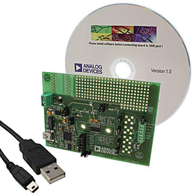
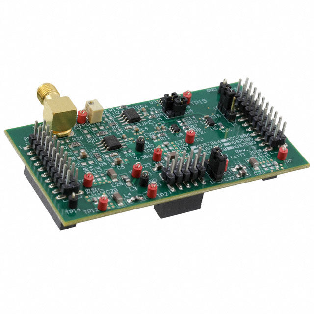
ICGOO电子元器件商城为您提供EVAL-AD7781EBZ由Analog设计生产,在icgoo商城现货销售,并且可以通过原厂、代理商等渠道进行代购。 EVAL-AD7781EBZ价格参考。AnalogEVAL-AD7781EBZ封装/规格:评估板 - 模数转换器(ADC), AD7781 - 20 Bit 470 Samples per Second Analog to Digital Converter (ADC) Evaluation Board。您可以下载EVAL-AD7781EBZ参考资料、Datasheet数据手册功能说明书,资料中有EVAL-AD7781EBZ 详细功能的应用电路图电压和使用方法及教程。
EVAL-AD7781EBZ是Analog Devices Inc.推出的一款评估板,专为AD7781模数转换器(ADC)设计。该评估板主要用于开发和测试AD7781 ADC的性能,适用于需要高精度、低功耗、小尺寸模数转换解决方案的应用场景。

典型应用场景包括:

1. 工业自动化与过程控制:用于传感器信号采集,如温度、压力、流量等模拟信号的数字化处理,适用于对精度和稳定性要求较高的工业环境。

2. 便携式仪器设备:由于AD7781具备低功耗特性,EVAL-AD7781EBZ适用于开发电池供电的便携式测量设备,如手持式测试仪表、数据采集系统等。

3. 医疗设备:可用于医疗监测设备中的生物信号采集,如心电图、血压监测等,满足对信号精度和噪声抑制的严格要求。

4. 智能传感器与物联网(IoT)节点:作为前端模数转换模块,用于各类物联网传感器节点中,实现对环境参数的高精度采集与传输。

5. 研发与教学实验:为工程师和研究人员提供便捷的硬件平台,用于评估AD7781的性能,进行算法验证和系统原型开发。

总之,EVAL-AD7781EBZ评估板广泛应用于需要高精度、低功耗ADC的各类电子系统开发中,尤其适合对空间和功耗有要求的嵌入式和便携式应用。
| 参数 | 数值 |
| ADC数 | 1 |
| 产品目录 | 编程器,开发系统嵌入式解决方案 |
| 描述 | BOARD EVAL FOR AD7781数据转换 IC 开发工具 EVAL BRD AD7781 |
| 产品分类 | 评估板 - 模数转换器 (ADC)工程工具 |
| 品牌 | Analog Devices Inc |
| 产品手册 | |
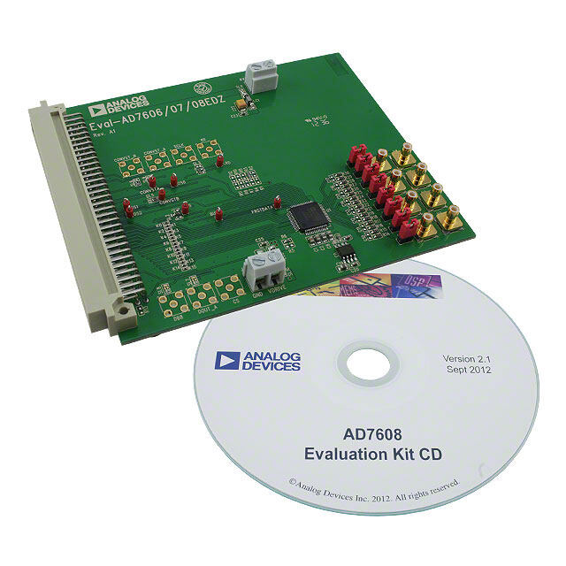
| 产品图片 |
|
| rohs | 符合RoHS无铅 / 符合限制有害物质指令(RoHS)规范要求 |
| 产品系列 | 模拟与数字IC开发工具,数据转换 IC 开发工具,Analog Devices EVAL-AD7781EBZ- |
| 数据手册 | |
| 产品型号 | EVAL-AD7781EBZ |
| 不同条件下的功率(典型值) | - |
| 产品 | Evaluation Boards |
| 产品种类 | 数据转换 IC 开发工具 |
| 位数 | 20 |
| 使用的IC/零件 | AD7781 |
| 其它名称 | EVALAD7781EBZ |
| 商标 | Analog Devices |
| 封装 | Bulk |
| 工作温度 | -40°C ~ 105°C |
| 工作电源电压 | 2.7 V to 5.25 V |
| 工具用于评估 | AD7781 |
| 工厂包装数量 | 1 |
| 所含物品 | 板 |
| 接口类型 | SPI |
| 数据接口 | SPI |
| 最大工作温度 | + 105 C |
| 最小工作温度 | - 40 C |
| 标准包装 | 1 |
| 类型 | ADC |
| 系列 | AD7781 |
| 输入范围 | ±5 V |
| 采样率(每秒) | 470 |


- 商务部:美国ITC正式对集成电路等产品启动337调查
- 曝三星4nm工艺存在良率问题 高通将骁龙8 Gen1或转产台积电
- 太阳诱电将投资9.5亿元在常州建新厂生产MLCC 预计2023年完工
- 英特尔发布欧洲新工厂建设计划 深化IDM 2.0 战略
- 台积电先进制程称霸业界 有大客户加持明年业绩稳了
- 达到5530亿美元!SIA预计今年全球半导体销售额将创下新高
- 英特尔拟将自动驾驶子公司Mobileye上市 估值或超500亿美元
- 三星加码芯片和SET,合并消费电子和移动部门,撤换高东真等 CEO
- 三星电子宣布重大人事变动 还合并消费电子和移动部门
- 海关总署:前11个月进口集成电路产品价值2.52万亿元 增长14.8%


PDF Datasheet 数据手册内容提取
20-Bit, Pin-Programmable, Low Power Sigma-Delta ADC AD7781 FEATURES FUNCTIONAL BLOCK DIAGRAM Pin-programmable filter response GND AVDD GAIN REFIN(+)REFIN(–) Update rate: 10 Hz or 16.7 Hz Pin-programmable in-amp gain AIN(+) DOUT/RDY G = 1 20-BIT Σ-Δ Pin-programmable power-down and reset OR 128 ADC Status function AIN(–) SCLK Internal clock oscillator DVDD BPDSW INTERNAL Internal bridge power-down switch CLOCK FILTER Cu1rr1e5n μt A typical (gain = 1) AD7781 PDRST 08162-001 Figure 1. 330 μA typical (gain = 128) Simultaneous 50 Hz/60 Hz rejection Table 1. Power supply: 2.7 V to 5.25 V Parameter Gain = 128 Gain = 1 −40°C to +105°C temperature range Output Data Rate 10 Hz 16.7 Hz 10 Hz 16.7 Hz Independent interface power supply RMS Noise Packages C Grade 44 nV 65 nV 2.4 μV 2.7 μV 14-lead, narrow body SOIC B Grade 55 nV 90 nV 2.4 μV 2.7 μV 16-lead TSSOP P-P Resolution 2-wire serial interface (read-only device) C Grade 17.6 17.1 18.8 18.7 SPI compatible B Grade 17.3 16.6 18.8 18.7 Schmitt trigger on SCLK Settling Time 300 ms 120 ms 300 ms 120 ms APPLICATIONS Weigh scales Pressure measurement Industrial process control Portable instrumentation GENERAL DESCRIPTION The AD7781 is a complete, low power front-end solution for The on-chip PGA has a gain of 1 or 128, supporting a full-scale bridge sensor products, including weigh scales, strain gages, differential input of ±5 V or ±39 mV. The device has two filter and pressure sensors. It contains a precision, low power, 20-bit response options. The filter response at the 16.7 Hz update rate sigma-delta (Σ-Δ) ADC, an on-chip, low noise programmable provides superior dynamic performance. The settling time is gain amplifier (PGA), and an on-chip oscillator. 120 ms at this update rate. At the 10 Hz update rate, the filter response provides better than −45 dB of stop-band attenuation. Consuming only 330 μA, the AD7781 is particularly suitable for In load cell applications, this stop-band rejection is useful to portable or battery-operated products where very low power is reject low frequency mechanical vibrations of the load cell. The required. The AD7781 also has a power-down mode that allows settling time is 300 ms at this update rate. Simultaneous 50 Hz/ the user to switch off the power to the bridge sensor and power 60 Hz rejection occurs at both the 10 Hz and 16.7 Hz update rates. down the AD7781 when not converting, thus increasing the battery life of the product. The AD7781 operates with a power supply from 2.7 V to 5.25 V. It is available in a narrow body, 14-lead SOIC package and in a For ease of use, all the features of the AD7781 are controlled by 16-lead TSSOP package. dedicated pins. Each time that a data read occurs, eight status bits are appended to the 20-bit conversion. These status bits contain a pattern sequence that can be used to confirm the validity of the serial transfer. Rev. 0 Information furnished by Analog Devices is believed to be accurate and reliable. However, no responsibility is assumed by Analog Devices for its use, nor for any infringements of patents or other One Technology Way, P.O. Box 9106, Norwood, MA 02062-9106, U.S.A. rights of third parties that may result from its use. Specifications subject to change without notice. No license is granted by implication or otherwise under any patent or patent rights of Analog Devices. Tel: 781.329.4700 www.analog.com Trademarks and registered trademarks are the property of their respective owners. Fax: 781.461.3113 ©2009 Analog Devices, Inc. All rights reserved.
AD7781 TABLE OF CONTENTS Features .............................................................................................. 1 Gain .............................................................................................. 11 Applications ....................................................................................... 1 Power-Down/Reset (PDRST) ................................................... 12 Functional Block Diagram .............................................................. 1 Analog Input Channel ............................................................... 12 General Description ......................................................................... 1 Bipolar Configuration ................................................................ 12 Revision History ............................................................................... 2 Data Output Coding .................................................................. 12 Specifications ..................................................................................... 3 Reference ..................................................................................... 12 Timing Characteristics ................................................................ 5 Bridge Power-Down Switch ...................................................... 12 Absolute Maximum Ratings ............................................................ 6 Digital Interface .......................................................................... 13 Thermal Resistance ...................................................................... 6 Applications Information .............................................................. 14 ESD Caution .................................................................................. 6 Weigh Scales ................................................................................ 14 Pin Configurations and Function Descriptions ........................... 7 AD7781 Performance in a Weigh Scale System ......................... 14 Typical Performance Characteristics ............................................. 8 EMI Recommendations ............................................................. 14 Output Noise and Resolution........................................................ 10 Grounding and Layout .............................................................. 15 Theory of Operation ...................................................................... 11 Outline Dimensions ....................................................................... 16 Filter, Data Rate, and Settling Time ......................................... 11 Ordering Guide .......................................................................... 16 REVISION HISTORY 5/09—Revision 0: Initial Version Rev. 0 | Page 2 of 16
AD7781 SPECIFICATIONS AV = 2.7 V to 5.25 V, V = AV , DV = 2.7 V to 5.25 V, GND = 0 V, all specifications T to T , unless otherwise noted.1 DD REF DD DD MIN MAX Table 2. Parameter Min Typ Max Unit Test Conditions/Comments ADC CHANNEL Output Update Rate (f ) 10 Hz FILTER = 1, settling time = 3/f ADC ADC 16.7 Hz FILTER = 0, settling time = 2/f ADC No Missing Codes2 20 Bits Resolution, Peak-to-Peak See Table 7 and Table 8 RMS Noise See Table 7 and Table 8 Integral Nonlinearity ±6 ppm FSR Offset Error ±6 μV Gain = 128 with FILTER = 1 ±200 μV Gain = 1 with FILTER = 1 ±1 μV Gain = 128 with FILTER = 0 ±10 μV Gain = 1 with FILTER = 0 Offset Error Drift vs. Temperature ±10 nV/°C Gain = 128 ±150 nV/°C Gain = 1 with FILTER = 1 ±10 nV/°C Gain = 1 with FILTER = 0 Full-Scale Error ±0.25 % of FS Gain Drift vs. Temperature ±2 ppm/°C Power Supply Rejection 100 dB Gain = 128, FILTER = 1, AIN = 7.81 mV 120 dB Gain = 128, FILTER = 0, AIN = 7.81 mV Normal Mode Rejection2 50 Hz, 60 Hz 63 75 dB 50 Hz ± 1 Hz, 60 Hz ± 1 Hz, f = 16.7 Hz ADC 72 90 dB 50 Hz ± 1 Hz, 60 Hz ± 1 Hz, f = 10 Hz ADC Common-Mode Rejection DC 90 dB Gain = 1, AIN = 1 V 90 dB Gain = 128, AIN = 7.81 mV 50 Hz, 60 Hz 110 dB 50 Hz ± 1 Hz, 60 Hz ± 1 Hz ANALOG INPUTS Differential Input Voltage Range ±V /gain V V = REFIN(+) − REFIN(−), REF REF gain = 1 or 128 Absolute AIN Voltage Limits2 GND + 100 mV AV − 100 mV V Gain = 1 DD GND + 450 mV AV − 1.1 V Gain = 128, FILTER = 0 DD GND + 1.1 AV − 1.1 V Gain = 128, FILTER = 1, AV ≤ 3.6 V DD DD GND + 1.5 AV − 1.5 V Gain = 128, FILTER = 1, AV > 3.6 V DD DD Average Input Current ±1 nA Gain = 1 ±250 pA Gain = 128 Average Input Current Drift ±3 pA/°C REFERENCE External REFIN Voltage AV V REFIN = REFIN(+) − REFIN(−) DD Reference Voltage Range2 0.5 AV V DD Absolute REFIN Voltage Limits2 GND − 30 mV AV + 30 mV V DD Average Reference Input Current 400 nA/V Average Reference Input Current ±0.15 nA/V/°C Drift Normal Mode Rejection Same as for analog inputs Common-Mode Rejection 110 dB BRIDGE POWER-DOWN SWITCH Controlled via the PDRST pin (BPDSW) R 9 Ω ON Allowable Current2 30 mA Continuous current Rev. 0 | Page 3 of 16
AD7781 Parameter Min Typ Max Unit Test Conditions/Comments INTERNAL CLOCK Frequency 64 − 3% 64 + 3% kHz Duty Cycle 50:50 % LOGIC INPUTS SCLK, FILTER, GAIN, PDRST2 Input Low Voltage, V 0.4 V DV = 3 V INL DD 0.8 V DV = 5 V DD Input High Voltage, V 1.8 V DV = 3 V INH DD 2.4 V DV = 5 V DD SCLK (Schmitt-Triggered Input) Hysteresis2 100 mV DV = 3 V DD 140 mV DV = 5 V DD Input Currents ±2 μA V = DV or GND IN DD Input Capacitance 10 pF All digital inputs LOGIC OUTPUT (DOUT/RDY) Output High Voltage, V 2 DV − 0.6 V DV = 3 V, I = 100 μA OH DD DD SOURCE 4 V DV = 5 V, I = 200 μA DD SOURCE Output Low Voltage, V 2 0.4 V DV = 3 V, I = 100 μA OL DD SINK 0.4 V DV = 5 V, I = 1.6 mA DD SINK Floating-State Leakage Current ±2 μA Floating-State Output Capacitance 10 pF Data Output Coding Offset binary POWER REQUIREMENTS3 Power Supply Voltage AV to GND 2.7 5.25 V DD DV to GND 2.7 5.25 V DD Power Supply Currents I Current DD Gain = 1 115 μA AV = 3 V DD 130 160 μA AV = 5 V DD Gain = 128 (B Grade) 300 μA AV = 3 V DD 350 400 μA AV = 5 V DD Gain = 128 (C Grade) 330 μA AV = 3 V DD 420 500 μA AV = 5 V DD I (Power-Down/Reset Mode) 10 μA DD 1 Temperature range is −40°C to +105°C. 2 This specification is not production tested but is supported by characterization data at initial product release. 3 Digital inputs are equal to DVDD or GND. Rev. 0 | Page 4 of 16
AD7781 TIMING CHARACTERISTICS AV = 2.7 V to 5.25 V, DV = 2.7 V to 5.25 V, GND = 0 V, Input Logic 0 = 0 V, Input Logic 1 = DV , unless otherwise noted. DD DD DD Table 3. Parameter1 Limit at T , T Unit Test Conditions/Comments MIN MAX Read2 t 100 ns min SCLK high pulse width 1 t 100 ns min SCLK low pulse width 2 t 3 0 ns min SCLK active edge to data valid delay4 3 60 ns max DV = 4.75 V to 5.25 V DD 80 ns max DV = 2.7 V to 3.6 V DD t 10 ns min SCLK inactive edge to DOUT/RDY high 4 130 ns max Reset t 100 ns min PDRST low pulse width 5 t 5 FILTER/GAIN change to data valid delay 6 120 ms typ Update rate = 16.7 Hz 300 ms typ Update rate = 10 Hz 1 Sample tested during initial release to ensure compliance. All input signals are specified with tR = tF = 5 ns (10% to 90% of DVDD) and timed from a voltage level of 1.6 V. 2 See Figure 3. 3 The values of t3 are measured using the load circuit of Figure 2 and are defined as the time required for the output to cross the VOL or VOH limits. 4 SCLK active edge is falling edge of SCLK. 5 The PDRST high to data valid delay is typically 1 ms longer than t6 because the internal oscillator requires time to power up and settle. Circuit and Timing Diagrams ISINK (1.6mA WITH DVDD = 5V, PDRST 100µA WITH DVDD = 3V) (INPUT) t 5 TO OUTPUT 1.6V PIN 50pF 1IS0O0UµRAC WE (IT20H0 DµAV DWDI T= H3 VD)VDD = 5V,08162-002 D(OOUUTT/PRUDTY) 08162-004 Figure 2. Load Circuit for Timing Characterization Figure 4. Resetting the AD7781 DOUT/RDY MSB LSB (OUTPUT) GAIN OR FILTER (INPUT) t t 3 4 t t 6 1 (INSPCULTK) t2 08162-003 D(OOUUTT/PRUDTY) 08162-005 Figure 3. Read Cycle Timing Diagram Figure 5. Changing Gain or Filter Option Rev. 0 | Page 5 of 16
AD7781 ABSOLUTE MAXIMUM RATINGS T = 25°C, unless otherwise noted. THERMAL RESISTANCE A θ is specified for the worst-case conditions, that is, a device Table 4. JA soldered in a circuit board for surface-mount packages. Parameter Rating AV to GND −0.3 V to +7 V DD Table 5. DV to GND −0.3 V to +7 V DD Package Type θ θ Unit JA JC Analog Input Voltage to GND −0.3 V to AV + 0.3 V DD 14-Lead SOIC 104.5 42.9 °C/W Reference Input Voltage to GND −0.3 V to AV + 0.3 V DD 16-Lead TSSOP 150.4 27.6 °C/W Digital Input Voltage to GND −0.3 V to DV + 0.3 V DD Digital Output Voltage to GND −0.3 V to DV + 0.3 V DD ESD CAUTION AIN/Digital Input Current 10 mA Operating Temperature Range −40°C to +105°C Storage Temperature Range −65°C to +150°C Maximum Junction Temperature 150°C Lead Temperature, Soldering Reflow 260°C Stresses above those listed under Absolute Maximum Ratings may cause permanent damage to the device. This is a stress rating only; functional operation of the device at these or any other conditions above those indicated in the operational section of this specification is not implied. Exposure to absolute maximum rating conditions for extended periods may affect device reliability. Rev. 0 | Page 6 of 16
AD7781 PIN CONFIGURATIONS AND FUNCTION DESCRIPTIONS NC 1 16 NC SCLK 1 14 FILTER SCLK 2 15 FILTER DOUT/RDY 2 13 PDRST DOUT/RDY 3 14 PDRST AGINAN(I+CN) 345 (NAToOtD Pto7 V 7SIE8caW1le) 111021 DAGVVNDDDDD GANICN 45 (NAToOtD Pto7 V 7SIE8caW1le) 1132 DAVVDDDD AIN(–) 6 9 BPDSW AIN(+) 6 11 GND REFIN(+) N7C = NO CONNECT8 REFIN(–) 08162-006 REAFIINN((+–)) 87NC = NO CONNECT190 BREPFDISNW(–) 08162-007 Figure 6. SOIC Pin Configuration Figure 7. TSSOP Pin Configuration Table 6. Pin Function Descriptions Pin No. SOIC TSSOP Mnemonic Description 1 2 SCLK Serial Clock Input. This serial clock input is for data transfers from the ADC. The SCLK pin has a Schmitt- triggered input. The serial clock can be active only when transferring data from the AD7781. The data from the AD7781 can be read as a continuous 32-bit word. Alternatively, SCLK can be noncontinuous during the data transfer, with the information being transmitted from the ADC in smaller data batches. 2 3 DOUT/RDY Serial Data Output/Data Ready Output. DOUT/RDY serves a dual purpose: as a data ready pin, going low to indicate the completion of a conversion, and as a serial data output pin to access the data register of the ADC. Eight status bits accompany each data read (see Figure 22). The DOUT/RDY falling edge can be used as an interrupt to a processor, indicating that new data is available. If the data is not read after the conversion, the pin goes high before the next update occurs. The serial interface is reset each time that a conversion is available. Therefore, the user must ensure that any conversions being transmitted are completed before the next conversion is available. 3 1, 4, 16 NC No Connect. This pin can be left floating. 4 5 GAIN Gain Select Pin. When GAIN is low, the gain is set to 128. When GAIN is high, the gain is set to 1. 5 6 AIN(+) Analog Input. AIN(+) is the positive terminal of the differential analog input pair, AIN(+)/AIN(−). 6 7 AIN(−) Analog Input. AIN(−) is the negative terminal of the differential analog input pair, AIN(+)/AIN(−). 7 8 REFIN(+) Positive Reference Input. An external reference can be applied between REFIN(+) and REFIN(−). The nomi- nal reference voltage (REFIN(+) − REFIN(−)) is 5 V, but the part can function with a reference of 0.5 V to AV . DD 8 9 REFIN(−) Negative Reference Input. 9 10 BPDSW Bridge Power-Down Switch to GND. When PDRST is high, the bridge power-down switch is closed. When PDRST is low, the switch is opened. 10 11 GND Ground Reference Point. 11 12 AV Supply Voltage, 2.7 V to 5.25 V. DD 12 13 DV Digital Interface Supply Voltage. The logic levels for the serial interface pins and the digital control pins DD are related to this supply, which is between 2.7 V and 5.25 V. The DV voltage is independent of the DD voltage on AV ; therefore, AV can equal 5 V with DV at 3 V or vice versa. DD DD DD 13 14 PDRST Power-Down/Reset. When this pin is low, the ADC is placed in power-down mode, and the low-side power switch is opened. All the logic on the chip is reset, and the DOUT/RDY pin is tristated. When PDRST is high, the ADC is taken out of power-down mode. The on-chip clock powers up and settles, and the ADC contin- uously converts. In addition, the low-side power switch is closed. The internal clock requires approximately 1 ms to power up. 14 15 FILTER Filter Select Pin. When FILTER is low, the fast settling filter is selected. The update rate is set to 16.7 Hz, which gives a filter settling time of 120 ms. When FILTER is high, the high rejection filter is selected. The update rate is set to 10 Hz, which gives a filter settling time of 300 ms. With this filter, the stop-band (higher than f ) attenuation is better than −45 dB. ADC Rev. 0 | Page 7 of 16
AD7781 TYPICAL PERFORMANCE CHARACTERISTICS 524,294 600 524,293 524,292 400 524,291 E C N E E D524,290 R O R C U C 524,289 OC 200 524,288 524,287 524,2860 200 400SAMPLE600 800 100008162-008 5204,275 524,277 COD5E24,279 MORE 08162-011 Figure 8. C Grade Noise (VREF = AVDD, Update Rate = 16.7 Hz, Gain = 128) Figure 11. C Grade Noise Distribution Histogram (VREF = AVDD, Update Rate = 10 Hz, Gain = 128) 500 524,289 400 524,288 E C300 N E E R D R O U C CC200 O 524,287 100 5204,286 524,288 5C24O,2D9E0 524,292 524,294 08162-009 524,2860 200 400SAMPLE600 800 100008162-012 Figure 9. C Grade Noise Distribution Histogram Figure 12. Noise (VREF = AVDD, Update Rate = 16.7 Hz, Gain = 1) (VREF = AVDD, Update Rate = 16.7 Hz, Gain = 128) 524,281 505 524,280 524,279 E C 524,278 N E E D R500 O R C524,277 CU C O 524,276 524,275 524,2740 200 400SAMPLE600 800 100008162-010 495 524,287 5C24O,D28E8 162-01308 Figure 10. C Grade Noise (VREF = AVDD, Update Rate = 10 Hz, Gain = 128) Figure 13. Noise Distribution Histogram (VREF = AVDD, Update Rate = 16.7 Hz, Gain = 1) Rev. 0 | Page 8 of 16
AD7781 524,276 2.0 1.5 1.0 524,275 S) 0.5 F CODE L (ppm 0 IN –0.5 524,274 –1.0 –1.5 524,2730 200 400SAMPLE600 800 100008162-014 –2.0–6 –4 –2 VIN0 (V) 2 4 608162-017 Figure 14. Noise (VREF = AVDD, Update Rate = 10 Hz, Gain = 1) Figure 17. Integral Nonlinearity (VREF = AVDD, Gain = 1) 800 10 8 6 600 4 CE V) 2 N µ RRE400 ET ( 0 OCCU OFFS –2 –4 200 –6 –8 0 524,274 5C2O4,D27E5 162-01508 –10–60 –40 –20 0TEMP2E0RATU4R0E (°C6)0 80 100 12008162-018 Figure 15. Noise Distribution Histogram Figure 18. Offset vs. Temperature (Gain = 128) (VREF = AVDD, Update Rate = 10 Hz, Gain = 1) 3.0 150 2.5 100 2.0 1.5 50 S) 1.0 ppm) L (ppm F 0.50 ERROR ( –500 IN–0.5 AIN G –1.0 –100 –1.5 –150 –2.0 –2.–50.04 –0.03 –0.02 –0.01 VIN0 (V) 0.01 0.02 0.03 0.0408162-016 –200–60 –40 –20 0TEMP2E0RATU4R0E (°C6)0 80 100 12008162-019 Figure 16. Integral Nonlinearity (VREF = AVDD, Gain = 128) Figure 19. Gain Error vs. Temperature (Gain = 128) Rev. 0 | Page 9 of 16
AD7781 OUTPUT NOISE AND RESOLUTION Table 7 and Table 8 show the rms noise of the AD7781 for the two output data rates and gain settings when using a 3 V and a 5 V reference. These numbers are typical and are generated with a differential input voltage of 0 V. The peak-to-peak (p-p) resolution is also listed. The p-p resolution represents the resolution for which there is no code flicker. These numbers are typical. Table 7. RMS Noise and Peak-to-Peak Resolution When AV = 3 V and V = 3 V DD REF Parameter Gain = 128 Gain = 1 Update Rate 10 Hz 16.7 Hz 10 Hz 16.7 Hz RMS Noise C Grade 44 nV 65 nV 2.4 μV 2.7 μV B Grade 55 nV 90 nV 2.4 μV 2.7 μV P-P Resolution C Grade 17.6 17.1 18.8 18.7 B Grade 17.3 16.6 18.8 18.7 Table 8. RMS Noise and Peak-to-Peak Resolution When AV = 5 V and V = 5 V DD REF Parameter Gain = 128 Gain = 1 Update Rate 10 Hz 16.7 Hz 10 Hz 16.7 Hz RMS Noise C Grade 49 nV 69 nV 3.0 μV 2.7 μV B Grade 60 nV 90 nV 3.0 μV 2.7 μV P-P Resolution C Grade 18.2 17.7 19.3 19.4 B Grade 17.9 17.3 19.3 19.4 Rev. 0 | Page 10 of 16
AD7781 THEORY OF OPERATION 0 The AD7781 is a low power ADC that incorporates a precision, 20-bit, Σ-Δ modulator; a PGA; and an on-chip digital filter –20 intended for measuring wide dynamic range, low frequency signals. The part provides a complete front-end solution for B) –40 bridge sensor applications such as weigh scales and pressure d N ( sensors. AI G –60 R The device has an internal clock and one buffered differential E T L input. It offers a choice of two update rates (10 Hz or 16.7 Hz) FI –80 and two gain settings (1 or 128). These functions are controlled using dedicated pins, which makes the interface easy to configure. –100 A 2-wire interface simplifies data retrieval from the AD7781. FTIhLeT AEDR7,7 D81A hTaAs t RwAo TfilEte,r A oNptDio nSsE. WTThLeInN thGe TFIIMLTEE R pin is –1200 20 INPU4T0 SIGNAL 6F0REQUENC80Y (Hz) 100 12008162-020 Figure 20. Filter Profile with Update Rate = 16.7 Hz (FILTER = 0) low, the 16.7 Hz filter is selected; when the FILTER pin is high, the 10 Hz filter is selected. When the polarity of the FILTER pin is changed, the AD7781 modulator and filter are reset immedi- 0 ately. DOUT/RDY is set high, and the ADC begins conversions using the selected filter response. The first conversion requires –20 the total settling time of the filter. Subsequent conversions occur at the selected update rate. The settling time of the 10 Hz B) –40 d filter is 300 ms (three conversion cycles), and the settling time N ( AI of the 16.7 Hz filter is 120 ms (two conversion cycles). R G –60 E T When a step change occurs on the analog input, the AD7781 L FI –80 requires several conversion cycles to generate a valid conversion. If the step change occurs synchronous to the conversion period, the –100 settling time of the AD7781 must be allowed to generate a valid conversion. If the step change occurs asynchronous to the end –120 oa fv aa lciodn cvoenrsvieornsi, oann. eTxhtrea d caotnav reergsiiostne rm isu ustp bdea atelldo wweitdh t aol lg ethnee rcaoten - 0 20 INPU4T0 SIGNAL 6F0REQUENC80Y (Hz) 100 12008162-021 Figure 21. Filter Profile with Update Rate = 10 Hz (FILTER = 1) versions, but, for an accurate result, the user must allow for the required time. GAIN Figure 20 and Figure 21 show the filter response for each filter. The AD7781 has two gain options: gain = 1 and gain = 128. The 10 Hz filter provides more than −45 dB of rejection in the When the GAIN pin is low, the gain is set to 128; when the stop band. The only external filtering required on the analog GAIN pin is high, the gain is set to 1. The acceptable analog inputs is a simple R-C filter to provide rejection at multiples of input range is ±VREF/gain. Thus, with VREF = 5 V, the input range the master clock. A 1 kΩ resistor in series with each analog input, is ±5 V when GAIN is high and ±39 mV when GAIN is low. a 0.01 μF capacitor from each input to GND, and a 0.1 μF When the polarity of the GAIN pin is changed, the AD7781 modu- capacitor from AIN(+) to AIN(−) are recommended. lator and filter are reset immediately. DOUT/RDY is set high, and When the filter is changed, DOUT/RDY goes high and remains the ADC begins conversions. DOUT/RDY remains high until high until the appropriate settling time for that filter elapses the appropriate settling time for the filter elapses (see Figure 5). (see Figure 5). Therefore, the user should complete any read Therefore, the user should complete any read operations before operations before changing the filter. Otherwise, 1s are read changing the gain. Otherwise, 1s are read back from the AD7781 back from the AD7781 because the DOUT/RDY pin is set high because the DOUT/RDY pin is set high following the gain change. following the filter change. The total settling time of the selected filter is required to generate the first conversion after the gain change; subsequent conversions occur at the selected update rate. Rev. 0 | Page 11 of 16
AD7781 POWER-DOWN/RESET (PDRST) The output code for any analog input voltage can be represented as The PDRST pin functions as a power-down pin and a reset pin. Code = 2N − 1 × [(AIN × Gain/VREF) + 1] When PDRST is taken low, the AD7781 is powered down. The where: entire ADC is powered down (including the on-chip clock), the AIN is the analog input voltage. low-side power switch is opened, and the DOUT/RDY pin is Gain is 1 or 128. tristated. The circuitry and serial interface are also reset, which N = 20. resets the logic, the digital filter, and the analog modulator. REFERENCE PDRST must be held low for 100 ns minimum to initiate the The AD7781 has a fully differential input capability for the channel. reset function (see Figure 4). The common-mode range for these differential inputs is GND to When PDRST is taken high, the AD7781 is taken out of power- AV . The reference input is unbuffered; therefore, excessive R-C DD down mode. When the on-chip clock has powered up (1 ms, source impedances introduce gain errors. The reference voltage of typically), the modulator begins sampling the analog input. REFIN (REFIN(+) − REFIN(−)) is AV nominal, but the AD7781 DD The low-side power switch is closed, and the DOUT/RDY pin is functional with reference voltages of 0.5 V to AV . In applica- DD becomes active. tions where the excitation (voltage or current) for the transducer A reset is automatically performed on power-up. on the analog input also drives the reference voltage for the part, the effect of the low frequency noise in the excitation source is ANALOG INPUT CHANNEL removed because the application is ratiometric. If the AD7781 The AD7781 has one differential analog input channel. The is used in a nonratiometric application, a low noise reference input channel feeds into a high impedance input stage of the should be used. amplifier. Therefore, the input can tolerate significant source Recommended 2.5 V reference voltage sources for the AD7781 impedances and is tailored for direct connection to external include the ADR381 and ADR391, which are low noise, low power resistive-type sensors such as strain gages. references. These references have low output impedances and The absolute input voltage range is restricted to a range between are, therefore, tolerant to decoupling capacitors on REFIN(+) GND + 450 mV and AVDD − 1.1 V. Care must be taken in setting without introducing gain errors in the system. Deriving the up the common-mode voltage to avoid exceeding these limits. reference input voltage across an external resistor means that Otherwise, there is degradation in linearity and noise performance. the reference input sees a significant external source impedance. External decoupling on the REFIN pins is not recommended in The low noise in-amp means that signals of small amplitude can this type of circuit configuration. be amplified within the AD7781, which still maintains excellent noise performance. The amplifier can be configured to have a gain BRIDGE POWER-DOWN SWITCH of 128 or 1, using the GAIN pin. The analog input range is equal The bridge power-down switch (BPDSW) is useful in battery- to ±V /gain. The common-mode voltage (AIN(+) + AIN(−))/2 REF powered applications where the optimization of system power must be ≥0.5 V. consumption is essential. A 350 Ω load cell typically consumes BIPOLAR CONFIGURATION 15 mA when excited with a 5 V power supply. To minimize current consumption, the load cell is disconnected when it is The AD7781 accepts a bipolar input range. A bipolar input range not being used. The bridge power-down switch can be included does not imply that the part can tolerate negative voltages with respect to system GND. Signals on the AIN(+) input are refer- in series with the load cell. When PDRST is high, the bridge power- enced to the voltage on the AIN(−) input. For example, if AIN(−) down switch is closed, and the load cell measures the strain. When is 2.5 V, the analog input range on the AIN(+) input is 2.46 V to PDRST is low, the bridge power-down switch is opened so no 2.54 V for a gain of 128. current flows through the load cell. Therefore, the current consumption of the system is minimized. The bridge power- DATA OUTPUT CODING down switch has an on resistance of 9 Ω maximum. The switch The AD7781 uses offset binary coding. Thus, a negative full- is capable of withstanding 30 mA of continuous current. scale voltage results in a code of 000...000, a zero differential input voltage results in a code of 100...000, and a positive full- scale input voltage results in a code of 111...111. Rev. 0 | Page 12 of 16
AD7781 DIGITAL INTERFACE When a conversion is complete, the serial interface is reset, and the new conversion is placed in the data register. Therefore, the The serial interface of the AD7781 consists of two signals: SCLK user must ensure that the complete word is read before the next and DOUT/RDY. SCLK is the serial clock input for the device, conversion is complete. and data transfers occur with respect to the SCLK signal. The DOUT/RDY pin is dual purpose: it functions as a data ready When PDRST is low, the DOUT/RDY pin is tristated. When pin and as a data output pin. DOUT/RDY goes low when a new PDRST is taken high, the internal clock requires approximately data-word is available in the output register. A 32-bit word is 1 ms to power up. Following power-up, the ADC continuously placed on the DOUT/RDY pin when sufficient SCLK pulses are converts. The first conversion requires the total settling time applied. This word consists of a 20-bit conversion result followed (see Figure 4). DOUT/RDY goes high when PDRST is taken by four 0s to generate a 24-bit word. Following this, status bits high and returns low only when a conversion is available. The are output. Figure 22 shows the status bits, and Table 9 describes ADC then converts continuously, and subsequent conversions the status bits and their functions. are available at the selected update rate. Figure 3 shows the timing for a read operation from the AD7781. RDY FILTER ERR ID1 ID0 GAIN PAT1 PAT0 08162-022 When the filter response is changed (using the FILTER pin) or Figure 22. Status Bits the gain is changed (using the GAIN pin), the modulator and DOUT/RDY is reset high when the conversion has been read. filter are reset immediately (see Figure 5). DOUT/RDY is set If the conversion is not read, DOUT/RDY goes high prior to the high. The ADC then begins conversions using the selected filter response/gain setting. DOUT/RDY remains high until the appro- data register update to indicate when not to read from the device. This ensures that a read operation is not attempted while the reg- priate settling time for that filter has elapsed. Therefore, the user ister is being updated. Each conversion can be read only once. The should complete any read operations before changing the gain or data register is updated for every conversion. update rate. Otherwise, 1s are read back from the AD7781 because the DOUT/RDY pin is set high following the gain/filter change. Table 9. Status Bit Functions Bit Name Description RDY Ready bit. 0: a conversion is available. FILTER Filter bit. 1: 10 Hz filter is selected. 0: 16.7 Hz filter is selected. ERR Error bit. 1: an error occurred during conversion. (An error occurs when the analog input is out of range.) ID1, ID0 ID bits. ID1 ID0 Function 0 0 Indicates the ID number for the AD7781. GAIN Gain bit. 1: gain = 1. 0: gain = 128. PAT1, PAT0 Status pattern bits. When the user reads data from the AD7781, a pattern check can be performed. PAT1 PAT0 Function 0 1 Indicates that the serial transfer from the ADC was performed correctly (default). 0 0 Indicates that the serial transfer from the ADC was not performed correctly. 1 x Indicates that the serial transfer from the ADC was not performed correctly. Rev. 0 | Page 13 of 16
AD7781 APPLICATIONS INFORMATION The AD7781 provides a low cost, high resolution analog-to- (the conversion result from the ADC when the maximum load digital function. Because the analog-to-digital function is is applied to the load cell) must be determined. Subsequent provided by a Σ-Δ architecture, the part is more immune to conversions from the AD7781 are then corrected, using the noisy environments, making it ideal for use in sensor measure- offset and gain coefficients that were calculated from these ment and industrial and process control applications. calibrations. WEIGH SCALES AD7781 PERFORMANCE IN A WEIGH SCALE SYSTEM Figure 23 shows the AD7781 being used in a weigh scale If the load cell has a sensitivity of 2 mV/V and a 5 V excitation application. The load cell is arranged in a bridge network and voltage is used, the full-scale signal from the load cell is 10 mV. gives a differential output voltage between its OUT+ and OUT− When the AD7781 (C grade) operates with a 10 Hz output data terminals. Assuming a 5 V excitation voltage, the full-scale rate and the gain is set to 128, the device has a p-p resolution of output range from the transducer is 10 mV when the sensitivity 18.2 bits when the reference is equal to 5 V. Postprocessing the is 2 mV/V. The excitation voltage for the bridge can be used to data from the AD7781 using a microprocessor increases the p-p directly provide the reference for the ADC because the refer- resolution. For example, an average by 4 in the microprocessor ence input range includes the supply voltage. increases the accuracy by 2 bits. The noise-free counts value is equal to A second advantage of using the AD7781 in transducer-based applications is that the bridge power-down switch (BPDSW) Noise-Free Counts = (2Effective Bits) × (FS /FS ) LC ADC can be fully utilized in low power applications. The bridge power- where: down switch is connected in series with the low side of the bridge. Effective Bits = 18.2 bits (AD7781) + 2 bits (due to postprocessing In normal operation, the switch is closed and measurements in the microprocessor). can be taken. In applications where power is of concern, the FS is the full-scale signal from the load cell (10 mV). LC AD7781 can be placed in power-down mode, significantly FS is the full-scale input range when gain = 128 and ADC reducing the power consumed in the application. In addition, V = 5 V (78 mV). REF the bridge power-down switch is opened while in power-down The noise-free counts is equal to mode, thus avoiding unnecessary power consumption by the front-end transducer. When the part is taken out of power-down (218.2 + 2) × (10 mV/78 mV) = 154,422 mode and the bridge power-down switch is closed, the user should This example shows that with a 5 V supply, 154,422 noise-free ensure that the front-end circuitry is fully settled before attempting counts can be achieved with the AD7781. to read from the AD7781. EMI RECOMMENDATIONS The load cell has an offset, or tare, associated with it. This tare is For simplicity, the EMI filters are not included in Figure 23. the main component of the system offset (load cell + ADC) and However, an R-C antialiasing filter should be included on each is similar in magnitude to the full-scale signal from the load cell. analog input. This filter is needed because the on-chip digital For this reason, calibrating the offset and gain of the AD7781 filter does not provide any rejection around the master clock or alone is not sufficient for optimum accuracy; a system calibration multiples of the master clock. Suitable values are a 1 kΩ resistor that calibrates the offset and gain of the ADC, plus the load cell, in series with each analog input, a 0.1 μF capacitor from AIN(+) is required. A microprocessor can be used to perform the calibra- to AIN(−), and 0.01 μF capacitors from AIN(+)/AIN(−) to GND. tions. The offset error (the conversion result from the AD7781 when no load is applied to the load cell) and the full-scale error VDD IN+ GND AVDD REFIN(+) OUT– OUT+ AIN(+) DOUT/RDY G = 1 20-BIT Σ-Δ IN– AIN(–) OR 128 ADC SCLK REFIN(–) INTERNAL DVDD CLOCK FILTER BPDSW PDRST AD7781 GAIN 8162-0230 Figure 23. Weigh Scales Using the AD7781 Rev. 0 | Page 14 of 16
AD7781 GROUNDING AND LAYOUT The ground plane of the AD7781 should be allowed to run under the AD7781 to prevent noise coupling. The power supply lines Because the analog input and reference input of the ADC are to the AD7781 should use as wide a trace as possible to provide differential, most of the voltages in the analog modulator are low impedance paths and reduce the effects of glitches on the common-mode voltages. The excellent common-mode reject- power supply line. Fast switching signals such as clocks should tion of the part removes common-mode noise on these inputs. be shielded with digital ground to avoid radiating noise to other The digital filter provides rejection of broadband noise on the sections of the board, and clock signals should never be run near power supply, except at integer multiples of the modulator the analog inputs. Avoid crossover of digital and analog signals. sampling frequency. The digital filter also removes noise from Traces on opposite sides of the board should run at right angles the analog and reference inputs, provided that these noise sources to each other. This reduces the effects of feedthrough through do not saturate the analog modulator. As a result, the AD7781 the board. A microstrip technique is by far the best, but it is not is more immune to noise interference than conventional high always possible with a double-sided board. In this technique, resolution converters. However, because the resolution of the the component side of the board is dedicated to ground planes, AD7781 is so high and the noise levels from the AD7781 are so and the signals are placed on the solder side. low, care must be taken with regard to grounding and layout. Good decoupling is important when using high resolution ADCs. The printed circuit board (PCB) that houses the AD7781 should AV should be decoupled with 10 μF tantalum capacitors in DD be designed so that the analog and digital sections are separated parallel with 0.1 μF capacitors to GND. DV should be decoupled DD and confined to certain areas of the board. A minimum etch with 10 μF tantalum capacitors in parallel with 0.1 μF capac- technique is generally best for ground planes because it gives itors to GND, with the system’s AGND to DGND connection the best shielding. being close to the AD7781. To achieve the best results from It is recommended that the GND pin of the AD7781 be tied these decoupling components, place them as close as possible to the AGND plane of the system. In any layout, pay attention to the device, ideally right up against the device. All logic chips to the flow of currents in the system and ensure that the return should be decoupled with 0.1 μF ceramic capacitors to DGND. paths for all currents are as close as possible to the paths that the currents took to reach their destinations. Avoid forcing digital currents to flow through the AGND sections of the layout. Rev. 0 | Page 15 of 16
AD7781 OUTLINE DIMENSIONS 8.75 (0.3445) 8.55 (0.3366) 4.00 (0.1575) 14 8 6.20 (0.2441) 3.80 (0.1496) 1 7 5.80 (0.2283) 1.27 (0.0500) 0.50 (0.0197) BSC 1.75 (0.0689) 0.25 (0.0098) 45° 0.25 (0.0098) 1.35 (0.0531) 8° 0.10 (0.0039) 0° COPLANARITY SEATING 0.10 0.51 (0.0201) PLANE 0.25 (0.0098) 1.27 (0.0500) 0.31 (0.0122) 0.17 (0.0067) 0.40 (0.0157) COMPLIANTTO JEDEC STANDARDS MS-012-AB (RCINEOFNPEATRRREOENNLCLTEIHN EOGSN EDLSIYM)AEANNRDSEI AORRNOESU NANORDEET DAIN-PO MPFRIFLO LMPIIMRLELIATIMTEEER TFSEO; RIRN ECUQHSU EDI VIINMA LEDENENSSTIIOGSN NFS.OR 060606-A Figure 24. 14-Lead Standard Small Outline Package [SOIC_N] Narrow Body (R-14) Dimensions shown in millimeters and (inches) 5.10 5.00 4.90 16 9 4.50 6.40 4.40 BSC 4.30 1 8 PIN 1 1.20 MAX 0.15 0.20 0.05 0.09 0.75 0.30 8° 0.60 0.65 0.19 SEATING 0° 0.45 BSC PLANE COPLANARITY 0.10 COMPLIANT TO JEDEC STANDARDS MO-153-AB Figure 25. 16-Lead Thin Shrink Small Outline Package [TSSOP] (RU-16) Dimensions shown in millimeters ORDERING GUIDE Model Temperature Range Package Description Package Option AD7781BRZ1 −40°C to +105°C 14-Lead SOIC_N R-14 AD7781BRZ-REEL1 −40°C to +105°C 14-Lead SOIC_N R-14 AD7781BRUZ1 −40°C to +105°C 16-Lead TSSOP RU-16 AD7781BRUZ-REEL1 −40°C to +105°C 16-Lead TSSOP RU-16 AD7781CRZ1 −40°C to +105°C 14-Lead SOIC_N R-14 AD7781CRZ-REEL1 −40°C to +105°C 14-Lead SOIC_N R-14 AD7781CRUZ1 −40°C to +105°C 16-Lead TSSOP RU-16 AD7781CRUZ-REEL1 −40°C to +105°C 16-Lead TSSOP RU-16 1 Z = RoHS Compliant Part. ©2009 Analog Devices, Inc. All rights reserved. Trademarks and registered trademarks are the property of their respective owners. D08162-0-5/09(0) Rev. 0 | Page 16 of 16
Mouser Electronics Authorized Distributor Click to View Pricing, Inventory, Delivery & Lifecycle Information: A nalog Devices Inc.: EVAL-AD7781EBZ AD7781CRZ-REEL AD7781BRZ AD7781CRUZ-REEL AD7781BRUZ-REEL AD7781BRZ-REEL AD7781CRUZ AD7781BRUZ AD7781CRZ