ICGOO在线商城 > 开发板,套件,编程器 > 评估板 - 模数转换器(ADC) > EVAL-AD7767-1EDZ
 Datasheet下载
- 型号: EVAL-AD7767-1EDZ
- 制造商: Analog
- 库位|库存: xxxx|xxxx
- 要求:
| 数量阶梯 | 香港交货 | 国内含税 |
| +xxxx | $xxxx | ¥xxxx |
查看当月历史价格
查看今年历史价格
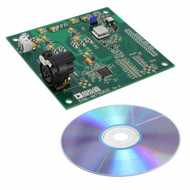
EVAL-AD7767-1EDZ产品简介:
ICGOO电子元器件商城为您提供EVAL-AD7767-1EDZ由Analog设计生产,在icgoo商城现货销售,并且可以通过原厂、代理商等渠道进行代购。 EVAL-AD7767-1EDZ价格参考。AnalogEVAL-AD7767-1EDZ封装/规格:评估板 - 模数转换器(ADC), AD7767-1 - 24 Bit 64k Samples per Second Analog to Digital Converter (ADC) Evaluation Board。您可以下载EVAL-AD7767-1EDZ参考资料、Datasheet数据手册功能说明书,资料中有EVAL-AD7767-1EDZ 详细功能的应用电路图电压和使用方法及教程。
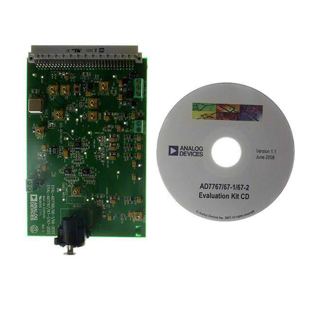
EVAL-AD7767-1EDZ 是 Analog Devices Inc. 提供的一款评估板,用于评估 AD7767-1 模数转换器(ADC)的性能和功能。该评估板主要应用于需要高精度、低功耗和高分辨率数据采集的场景。以下是其典型的应用场景:

 1. 工业自动化与控制
   - 在工业自动化领域,EVAL-AD7767-1EDZ 可用于传感器信号的精确采集,例如压力、温度、振动等物理量的测量。
   - 适用于工业 PLC(可编程逻辑控制器)、数据采集系统(DAQ)以及远程监控设备。

 2. 医疗设备
   - 高精度 ADC 适合用于医疗设备中的信号采集,如心电图(ECG)、脑电图(EEG)和超声波成像设备。
   - 其低噪声和高分辨率特性能够确保生物电信号的准确捕捉和处理。

 3. 能源管理
   - 在智能电网、电力监测和能源管理系统中,该评估板可用于电压、电流和功率的高精度测量。
   - 特别适用于三相电能表、太阳能逆变器和其他需要精确能量计量的场合。

 4. 环境监测
   - EVAL-AD7767-1EDZ 可用于环境监测系统,例如空气质量监测、水质量检测和气象站。
   - 能够精确采集来自各种传感器的数据,如气体浓度、湿度、光照强度等。

 5. 音频处理
   - AD7767-1 的高分辨率和低失真特性使其适合音频信号的数字化处理,例如专业音频设备、麦克风阵列和声音分析仪。

 6. 汽车电子
   - 在汽车电子领域,该评估板可用于电池管理系统(BMS)、车载传感器数据采集以及发动机控制单元(ECU)中。
   - 提供对车辆关键参数(如电池电压、电流、温度等)的高精度测量。

 7. 科学仪器
   - 科学研究中需要高精度数据采集时,EVAL-AD7767-1EDZ 是理想选择,例如光谱分析仪、示波器和其他精密测量设备。

通过 EVAL-AD7767-1EDZ 评估板,用户可以方便地测试 AD7767-1 ADC 的性能指标(如采样率、信噪比、线性度等),并验证其在实际应用中的表现,从而加速产品开发过程。
| 参数 | 数值 |
| ADC数 | 1 |
| 产品目录 | 编程器,开发系统嵌入式解决方案 |
| 描述 | BOARD EVAL AD7767-1 64KSPS 111DB数据转换 IC 开发工具 EVAL-AD7767-1 |
| 产品分类 | 评估板 - 模数转换器 (ADC)工程工具 |
| 品牌 | Analog Devices |
| 产品手册 | |
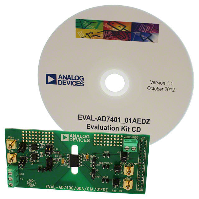
| 产品图片 |
|
| rohs | 符合RoHS无铅 / 符合限制有害物质指令(RoHS)规范要求 |
| 产品系列 | 模拟与数字IC开发工具,数据转换 IC 开发工具,Analog Devices EVAL-AD7767-1EDZ- |
| 数据手册 | |
| 产品型号 | EVAL-AD7767-1EDZ |
| 不同条件下的功率(典型值) | 10.5mW @ 64kSPS |
| 产品 | Evaluation Boards |
| 产品种类 | 数据转换 IC 开发工具 |
| 位数 | 24 |
| 使用的IC/零件 | AD7767-1 |
| 其它名称 | EVALAD77671EDZ |
| 商标 | Analog Devices |
| 封装 | Bulk |
| 工作温度 | -40°C ~ 105°C |
| 工作电源电压 | 2.375 V to 2.625 V |
| 工具用于评估 | AD7767 |
| 工厂包装数量 | 1 |
| 所含物品 | 板 |
| 接口类型 | Serial |
| 数据接口 | 串行 |
| 最大工作温度 | + 105 C |
| 最小工作温度 | - 40 C |
| 标准包装 | 1 |
| 相关产品 | /product-detail/zh/AD7767BRUZ-2/AD7767BRUZ-2-ND/1680413/product-detail/zh/AD7767BRUZ-1/AD7767BRUZ-1-ND/1680412/product-detail/zh/AD7767BRUZ/AD7767BRUZ-ND/1680411/product-detail/zh/AD7767BRUZ-RL7/AD7767BRUZ-RL7-ND/1679876/product-detail/zh/AD7767BRUZ-2-RL7/AD7767BRUZ-2-RL7-ND/1679875/product-detail/zh/AD7767BRUZ-1-RL7/AD7767BRUZ-1-RL7-ND/1679874 |
| 类型 | ADC |
| 系列 | AD7767 |
| 输入范围 | ±VREF |
| 采样率(每秒) | 64k |


- 商务部:美国ITC正式对集成电路等产品启动337调查
- 曝三星4nm工艺存在良率问题 高通将骁龙8 Gen1或转产台积电
- 太阳诱电将投资9.5亿元在常州建新厂生产MLCC 预计2023年完工
- 英特尔发布欧洲新工厂建设计划 深化IDM 2.0 战略
- 台积电先进制程称霸业界 有大客户加持明年业绩稳了
- 达到5530亿美元!SIA预计今年全球半导体销售额将创下新高
- 英特尔拟将自动驾驶子公司Mobileye上市 估值或超500亿美元
- 三星加码芯片和SET,合并消费电子和移动部门,撤换高东真等 CEO
- 三星电子宣布重大人事变动 还合并消费电子和移动部门
- 海关总署:前11个月进口集成电路产品价值2.52万亿元 增长14.8%


PDF Datasheet 数据手册内容提取
24-Bit, 8.5 mW, 109 dB, 128 kSPS/64 kSPS/32 kSPS ADCs AD7767 FEATURES GENERAL DESCRIPTION Oversampled successive approximation (SAR) architecture The AD7767/AD7767-1/AD7767-2 are high performance, High performance ac and dc accuracy, low power 24-bit, oversampled SAR analog-to-digital converters (ADCs). 115.5 dB dynamic range, 32 kSPS (AD7767-2) The AD7767/AD7767-1/AD7767-2 combine the benefits of a 112.5 dB dynamic range, 64 kSPS (AD7767-1) large dynamic range and input bandwidth, consuming 15 mW, 109.5 dB dynamic range, 128 kSPS (AD7767) 10.5 mW, and 8.5 mW power, respectively, and are contained in −118 dB THD a 16-lead TSSOP package. Exceptionally low power Ideal for ultralow power data acquisition (such as PCI- and 8.5 mW, 32 kSPS (AD7767-2) USB-based systems), the AD7767/AD7767-1/AD7767-2 10.5 mW, 64 kSPS (AD7767-1) provide 24-bit resolution. The combination of exceptional SNR, 15 mW, 128 kSPS (AD7767) wide dynamic range, and outstanding dc accuracy make the High dc accuracy AD7767/AD7767-1/AD7767-2 ideally suited for measuring 24 bits, no missing codes (NMC) small signal changes over a wide dynamic range. This is INL: ±3 ppm (typical), ±7.6 ppm (maximum) particularly suitable for applications where small changes on the Low temperature drift input are measured on larger ac or dc signals. In such an Zero error drift: 15 nV/°C application, the AD7767/AD7767-1/AD7767-2 accurately Gain error drift: 0.4 ppm/°C gather both ac and dc information. On-chip low-pass FIR filter Linear phase response The AD7767/AD7767-1/AD7767-2 include an on-board digital Pass-band ripple: ±0.005 dB filter (complete with linear phase response) that acts to elimi- Stop-band attenuation: 100 dB nate out-of-band noise by filtering the oversampled input 2.5 V supply with 1.8 V/2.5 V/3 V/3.6 V logic interface options voltage. The oversampled architecture also reduces front-end Flexible interfacing options antialias requirements. Other features of the AD7767 include a Synchronization of multiple devices SYNC/PD (synchronization/power-down) pin, allowing the Daisy-chain capability synchronization of multiple AD7767 devices. The addition of Power-down function an SDI pin provides the option of daisy chaining multiple Temperature range: −40°C to +105°C AD7767 devices. APPLICATIONS The AD7767/AD7767-1/AD7767-2 operate from a 2.5 V supply using a 5 V reference. The devices operate from −40°C to +105°C. Low power PCI/USB data acquisition systems Low power wireless acquisition systems RELATED DEVICES Vibration analysis Table 1. 24-Bit ADCs Instrumentation Part No. Description High precision medical acquisition AD7760 2.5 MSPS, 100 dB dynamic range,1 on-board differential FUNCTIONAL BLOCK DIAGRAM amp and reference buffer, parallel, variable decimation AVDD AGND MCLK DVDD VDRIVE DGND AD7762/ 625 kSPS, 109 dB dynamic range,1 on-board differential AD7763 amp and reference buffer, parallel/serial, variable VREF+ decimation VIN+ AD7764 312 kSPS, 109 dB dynamic range,1 on-board differential SUCCESSIVE DIGITAL amp and reference buffer, variable decimation (pin) APPROXIMATION FIR FILTER ADC AD7765 156 kSPS, 112 dB dynamic range,1 on-board differential VIN– SYNC/PD amp and reference buffer, variable decimation (pin) SERIAL INTERFACE REFGND AND CS AD7766 128 kSPS, 109.5 dB,1 15 mW, 16-bit INL, serial interface AD7767/ CONTROL LOGIC AD7766-1 64 kSPS 112.5 dB,110.5 mW, 16-bit INL, serial interface AD7767-1/ AD7767-2 AD7766-2 32 kSPS, 115.5 dB,1 8.5 mW, 16-bit INL, serial interface SCLKDRDY SDO SDI 06859-001 1 Dynamic range at maximum output data rate. Figure 1. Rev. C Information furnished by Analog Devices is believed to be accurate and reliable. However, no responsibility is assumed by Analog Devices for its use, nor for any infringements of patents or other One Technology Way, P.O. Box 9106, Norwood, MA 02062-9106, U.S.A. rights of third parties that may result from its use. Specifications subject to change without notice. No license is granted by implication or otherwise under any patent or patent rights of Analog Devices. Tel: 781.329.4700 www.analog.com Trademarks and registered trademarks are the property of their respective owners. Fax: 781.461.3113 ©2007–2010 Analog Devices, Inc. All rights reserved.
AD7767 TABLE OF CONTENTS Features .............................................................................................. 1 Supply and Reference Voltages ................................................. 16 Applications ....................................................................................... 1 AD7767 Interface ........................................................................... 17 Functional Block Diagram .............................................................. 1 Initial Power-Up ......................................................................... 17 General Description ......................................................................... 1 Reading Data ............................................................................... 17 Related Devices ................................................................................. 1 Power-Down, Reset, and Synchronization ............................. 17 Revision History ............................................................................... 2 Daisy Chaining ............................................................................... 18 Specifications ..................................................................................... 3 Reading Data in Daisy-Chain Mode ....................................... 18 Timing Specifications .................................................................. 5 Choosing the SCLK Frequency ................................................ 18 Timing Diagrams .......................................................................... 6 Daisy-Chain Mode Configuration and Timing Diagrams ... 19 Absolute Maximum Ratings ............................................................ 8 Driving the AD7767 ....................................................................... 20 ESD Caution .................................................................................. 8 Differential Signal Source ......................................................... 20 Pin Configuration and Function Descriptions ............................. 9 Single-Ended Signal Source ...................................................... 20 Typical Performance Characteristics ........................................... 10 Antialiasing ................................................................................. 21 Terminology .................................................................................... 14 Power Dissipation....................................................................... 21 Theory of Operation ...................................................................... 15 V Input Signal ....................................................................... 22 REF+ AD7767/AD7767-1/AD7767-2 Transfer Function ................ 15 Multiplexing Analog Input Channels ...................................... 22 Converter Operation .................................................................. 15 Outline Dimensions ....................................................................... 23 Analog Input Structure .............................................................. 16 Ordering Guide .......................................................................... 23 REVISION HISTORY 5/10—Rev. B to Rev. C Changes to Pin 8 Description ......................................................... 9 Changes to Table 8 .......................................................................... 20 3/09—Rev. A to Rev. B Changes to t Parameter, Table 3 .......................................... 5 SETTLING Changes to Table 7 .......................................................................... 17 1/09—Rev. 0 to Rev. A Changes to Features Section............................................................ 1 Change to Intermodulation Distortion (IMD) Parameter and Integral Nonlinearity Parameter, Table 2 ................................. 3 Changes to Supply and Reference Voltages Section ................... 16 Changes to Choosing the SCLK Frequency Section .................. 18 Changes to Figure 24 ...................................................................... 12 Changes to Driving the AD7767 Section .................................... 20 Changes to Single-Ended Signal Source Section ........................ 20 Added Figure 41; Renumbered Sequentially .............................. 20 Change to Figure 42 ....................................................................... 21 Added Table 8; Renumbered Sequentially .................................. 20 Replaced V Input Signal Section ............................................ 22 REF+ Replaced Figure 46 ......................................................................... 22 8/07—Revision 0: Initial Version Rev. C | Page 2 of 24
AD7767 SPECIFICATIONS AV = DV = 2.5 V ± 5%, V = 1.8 V to 3.6 V, V = 5 V, MCLK = 1 MHz, common-mode input = V /2, T = −40°C to +105°C, DD DD DRIVE REF REF A unless otherwise noted. Table 2. Parameter Test Conditions/Comments Min Typ Max Unit OUTPUT DATA RATE (ODR) AD7767 Decimate by 8 128 kHz AD7767-1 Decimate by 16 64 kHz AD7767-2 Decimate by 32 32 kHz ANALOG INPUT1 Differential Input Voltage V − V ±V V p-p IN+ IN− REF Absolute Input Voltage V −0.1 +V + 0.1 V IN+ REF V −0.1 +V + 0.1 V IN− REF Common-Mode Input Voltage V /2 − 5% V /2 V /2 + 5% V REF REF REF Input Capacitance 22 pF DYNAMIC PERFORMANCE AD7767 Decimate by 8, ODR = 128 kHz Dynamic Range2 Shorted inputs 108 109.5 dB Signal-to-Noise Ratio (SNR)2 Full-scale input amplitude, 1 kHz tone 107 108.5 dB Spurious-Free Dynamic Range (SFDR)2 Full-scale input amplitude, 1 kHz tone −128 −116 dB Total Harmonic Distortion (THD)2 Full-scale input amplitude, 1 kHz tone −118 −105 dB Intermodulation Distortion (IMD)2 Tone A = 49.7 kHz, Tone B = 50.3 kHz Second-Order Terms −133 dB Third-Order Terms −109 dB AD7767-1 Decimate by 16, ODR = 64 kHz Dynamic Range2 Shorted inputs 111 112.5 dB Signal-to-Noise Ratio (SNR)2 Full-scale input amplitude, 1 kHz tone 110 111.5 dB Spurious-Free Dynamic Range (SFDR)2 Full-scale input amplitude, 1 kHz tone −128 −116 dB Total Harmonic Distortion (THD)2 Full-scale input amplitude, 1 kHz tone −118 −105 dB Intermodulation Distortion (IMD)2 Tone A = 24.7 kHz, Tone B = 25.3 kHz dB Second-Order Terms −133 dB Third-Order Terms −108 dB AD7767-2 Decimate by 32, ODR = 32 kHz Dynamic Range2 Shorted inputs 114 115.5 dB Signal-to-Noise Ratio (SNR)2 Full-scale input amplitude, 1 kHz tone 112 113.5 dB Spurious-Free Dynamic Range (SFDR)2 Full-scale input amplitude, 1 kHz tone −128 −116 dB Total Harmonic Distortion (THD)2 Full-scale input amplitude, 1 kHz tone −118 −105 dB Intermodulation Distortion (IMD)2 Tone A = 11.7 kHz, Tone B = 12.3 kHz dB Second-Order Terms −137 dB Third-Order Terms −108 dB DC ACCURACY1 For all devices Resolution No missing codes 24 Bits Differential Nonlinearity2 Guaranteed monotonic to 24 bits Integral Nonlinearity2 18-bit linearity ±3 ±7.6 ppm Zero Error2 20 μV Gain Error2 0.0075 0.075 % FS Zero Error Drift2 15 nV/°C Gain Error Drift2 0.4 ppm/°C Common-Mode Rejection Ratio2 50 Hz tone −110 dB Rev. C | Page 3 of 24
AD7767 Parameter Test Conditions/Comments Min Typ Max Unit DIGITAL FILTER RESPONSE1 Group Delay 37/ODR μs Settling Time (Latency) Complete settling 74/ODR μs Pass-Band Ripple ±0.005 dB Pass Band 0.453 × ODR Hz −3 dB Bandwidth 0.49 × ODR Hz Stop-Band Frequency 0.547 × ODR Hz Stop-Band Attenuation 100 dB REFERENCE INPUT1 V Input Voltage 2.4 2 × AV V REF+ DD DIGITAL INPUTS (Logic Levels)1 V −0.3 +0.3 × V V IL DRIVE V 0.7 × V V + 0.3 V IH DRIVE DRIVE Input Leakage Current ±1 μA/pin Input Capacitance 5 pF Master Clock Rate 1.024 MHz Serial Clock Rate 1/t Hz 8 DIGITAL OUTPUTS1 Data Format Serial 24 bits, twos complement (MSB first) V I = +500 μA 0.4 V OL SINK V I = −500 μA V – 0.3 V OH SOURCE DRIVE POWER REQUIREMENTS1 AV ± 5% 2.5 V DD DV ± 5% 2.5 V DD V 1.7 2.5 3.6 V DRIVE CURRENT SPECIFICATIONS MCLK = 1.024 MHz AD7767 Operational Current 128 kHz output data rate AI 1.3 1.5 mA DD DI 3.9 4.8 mA DD I 0.35 0.425 mA REF AD7767-1 Operational Current 64 kHz output data rate AI 1.3 1.5 mA DD DI 2.2 2.85 mA DD I 0.35 0.425 mA REF AD7767-2 Operational Current 32 kHz output data rate AI 1.3 1.5 mA DD DI 1.37 1.86 mA DD I 0.35 0.425 mA REF Static Current with MCLK Stopped For all devices AI 0.9 1 mA DD DI 1 93 μA DD Power-Down Mode Current For all devices AI 0.1 6 μA DD DI 1 93 μA DD POWER DISSIPATION MCLK = 1.024 MHz AD7767 Operational Power 128 kHz output data rate 15 18 mW AD7767-1 Operational Power 64 kHz output data rate 10.5 13 mW AD7767-2 Operational Power 32 kHz output data rate 8.5 10.5 mW 1 Specifications are for all devices, AD7767, AD7767-1, and AD7767-2. 2 See the Terminology section. Rev. C | Page 4 of 24
AD7767 TIMING SPECIFICATIONS AV = DV = 2.5 V ± 5%, V = 1.7 V to 3.6 V, V = 5 V, common-mode input = V /2, T = −40°C (T ) to +105°C (T ), DD DD DRIVE REF REF A MIN MAX unless otherwise noted.1 Table 3. Parameter Limit at t , t Unit Description MIN MAX DRDY OPERATION t 510 ns typ MCLK rising edge to DRDY falling edge 1 t 2 100 ns min MCLK high pulse width 2 t2 900 ns max MCLK low pulse width 3 t 265 ns typ MCLK rising edge to DRDY rising edge (AD7767) 4 128 ns typ MCLK rising edge to DRDY rising edge (AD7767-1) 71 ns typ MCLK rising edge to DRDY rising edge (AD7767-2) t 294 ns typ DRDY pulse width (AD7767) 5 435 ns typ DRDY pulse width (AD7767-1) 492 ns typ DRDY pulse width (AD7767-2) t 3 t − t ns typ DRDY low period, read data during this period READ DRDY 5 t 3 n × 8 × t ns typ DRDY period DRDY MCLK Read OPERATION t 0 ns min DRDY falling edge to CS setup time 6 t 6 ns max CS falling edge to SDO tristate disabled 7 t 60 ns max Data access time after SCLK falling edge (V = 1.7 V) 8 DRIVE 50 ns max Data access time after SCLK falling edge (V = 2.3 V) DRIVE 25 ns max Data access time after SCLK falling edge (V = 2.7 V) DRIVE 24 ns max Data access time after SCLK falling edge (V = 3.0 V) DRIVE t 10 ns min SCLK falling edge to data valid hold time (V = 3.6 V) 9 DRIVE t 10 ns min SCLK high pulse width 10 t 10 ns min SCLK low pulse width 11 t 1/t sec min Minimum SCLK period SCLK 8 t 6 ns max Bus relinquish time after CS rising edge 12 t 0 ns min CS rising edge to DRDY rising edge 13 Read OPERATION WITH CS LOW t 0 ns min DRDY falling edge to data valid setup time 14 t 0 ns max DRDY rising edge to data valid hold time 15 DAISY-CHAIN OPERATION t 1 ns min SDI valid to SCLK falling edge setup time 16 t 2 ns max SCLK falling edge to SDI valid hold time 17 SYNC/PD OPERATION t 1 ns typ SYNC/PD falling edge to MCLK rising edge 18 t 20 ns typ MCLK rising edge to DRDY rising edge going into SYNC/PD mode 19 t 1 ns min SYNC/PD rising edge to MCLK rising edge 20 t 510 ns typ MCLK rising edge to DRDY falling edge coming out of SYNC/PD mode 21 t 3 (592 × n) + 2 t Filter settling time after a reset or power-down SETTLING MCLK 1 Sample tested during initial release to ensure compliance. All input signals are specified with tr = tf = 5 ns (10% to 90% of DVDD) and timed from a voltage level of 1.7 V. 2 t2 and t3 allow a ~90% to 10% duty cycle to be used for the MCLK input, where the minimum is 10% for the clock high time and 90% for MCLK low time. The maximum MCLK frequency is 1.024 MHz. 3 n = 1 for AD7767, n = 2 for the AD7767-1, n = 4 for the AD7767-2. Rev. C | Page 5 of 24
AD7767 TIMING DIAGRAMS t 2 MCLK 1 8 × n 1 8 × n t3 t4 t t t 1 5 5 t DRDY READ tDRDY 06859-002 Figure 2. DRDY vs. MCLK Timing Diagram, n = 1 for AD7767 (Decimate by 8), n = 2 for AD7767-1 (Decimate by 16), n = 4 for AD7767-2 (Decimate by 32) t DRDY DRDY tREAD t t 13 6 CS t 10 1 23 SCLK t t8 t9 t11 7 t 12 SDO MSB D22 D21 D20 D1 LSB 06859-003 Figure 3. Serial Timing Diagram, Reading Data Using CS CS = 0 t DRDY DRDY tREAD t 14 t 10 SCLK 1 23 24 t 11 t t t 8 9 15 SDO INDVAATLAID MSB D22 D21 D20 D1 LSB INDVAATLAID 06859-004 Figure 4. Serial Timing Diagram, Reading Data Setting CS Logic Low Rev. C | Page 6 of 24
AD7767 PART OUT OF POWER-DOWN FILTER RESET PART IN POWER-DOWN BEGINS SAMPLING MCLK (I) A B C D t18 t20 SYNC/PD (I) t19 t21 DRDY (O) tSETTLING DOUT (O) VALID DATA INVALID DATA VALID DATA 06859-005 Figure 5. Reset, Synchronization, and Power-Down Timing (For More Information, See the Power-Down, Reset, and Synchronization Section) Rev. C | Page 7 of 24
AD7767 ABSOLUTE MAXIMUM RATINGS T = 25°C, unless otherwise noted. A Table 4. Stresses above those listed under Absolute Maximum Ratings Parameter Rating may cause permanent damage to the device. This is a stress AV to AGND −0.3 V to +3 V DD rating only; functional operation of the device at these or any DV to DGND −0.3 V to +3 V DD other conditions above those indicated in the operational AV to DV −0.3 V to +0.3 V DD DD section of this specification is not implied. Exposure to absolute V to REFGND −0.3 V to +7 V REF+ maximum rating conditions for extended periods may affect REFGND to AGND −0.3 V to +0.3 V device reliability. V to DGND −0.3 V to +6 V DRIVE V ,V to AGND −0.3 V to V + 0.3 V ESD CAUTION IN+ IN– REF+ Digital Inputs to DGND −0.3 V to V + 0.3 V DRIVE Digital Outputs to DGND −0.3 V to V + 0.3 V DRIVE AGND to DGND −0.3 V to +0.3 V Input Current to Any Pin Except ±10 mA Supplies1 Operating Temperature Range −40°C to +105°C Storage Temperature Range −65°C to +150°C Junction Temperature 150°C TSSOP Package θ Thermal Impedance 150.4°C/W JA θ Thermal Impedance 27.6°C/W JC Lead Temperature, Soldering Vapor Phase (60 sec) 215°C Infrared (15 sec) 220°C ESD 1 kV 1 Transient currents of up to 100 mA do not cause SCR latch-up. Rev. C | Page 8 of 24
AD7767 PIN CONFIGURATION AND FUNCTION DESCRIPTIONS AVDD 1 16 CS VREF+ 2 15 SDI AD7767/ REFGND 3 14 MCLK AD767-1/ VIN+ 4 AD7767-2 13 SCLK VIN– 5 (NToOt Pto V SIEcaWle) 12 DRDY AGND 6 11 DGND SYNC/PD 7 10 SDO DVDD 8 9 VDRIVE 06859-006 Figure 6. 16-Lead TSSOP Pin Configuration Table 5. Pin Function Descriptions Pin No. Mnemonic Description 1 AV +2.5 V Analog Power Supply. DD 2 V Reference Input for the AD7767. An external reference must be applied to this input pin. The V input can range REF+ REF+ from 2.4 V to 5 V. The reference voltage input is independent of the voltage magnitude applied to the AV pin. DD 3 REFGND Reference Ground. Ground connection for the reference voltage. The input reference voltage (V ) should be REF+ decoupled to this pin. 4 V Positive Input of the Differential Analog Input. IN+ 5 V Negative Input of the Differential Analog Input. IN− 6 AGND Power Supply Ground for Analog Circuitry. 7 SYNC/PD Synchronization and Power-Down Input Pin. This pin has dual functionality. It can be used to synchronize multiple AD7767 devices and/or to put the AD7767 device into power-down mode. See the Power-Down, Reset, and Synchronization section for further details. 8 DV 2.5 V Digital Power Supply Input. In cases where an logic voltage of 2.5 V is used for interfacing (2.5 V applied to DD V pin), the DVDD and V pin may be connected to the same voltage supply rail. DRIVE DRIVE 9 V Logic Power Supply Input, 1.8 V to 3.6 V. The voltage supplied at this pin determines the operating voltage of the DRIVE digital logic interface. 10 SDO Serial Data Output. The conversion result from the AD7767 is output on the SDO pin as a 24-bit, twos complement, MSB first, serial data stream. 11 DGND Digital Logic Power Supply Ground. 12 DRDY Data Ready Output. A falling edge on the DRDY signal indicates that a new conversion data result is available in the output register of the AD7767. See the AD7767 Interface section for further details. 13 SCLK Serial Clock Input. The SCLK input provides the serial clock for all serial data transfers with the AD7767 device. See the AD7767 Interface section for further details. 14 MCLK Master Clock Input. The AD7767 sampling frequency is equal to the MCLK frequency. 15 SDI Serial Data Input. This is the daisy-chain input of the AD7767. See the Daisy Chaining section for further details. 16 CS Chip Select Input. The CS input selects the AD7767 device and acts as an enable on the SDO pin. In cases where CS is used, the MSB of the conversion result is clocked onto the SDO line on the CS falling edge. The CS input allows multiple AD7767 devices to share the same SDO line. This allows the user to select the appropriate device by supplying it with a logic low CS signal, which enables the SDO pin of the device concerned. See the AD7767 Interface section for further details. Rev. C | Page 9 of 24
AD7767 TYPICAL PERFORMANCE CHARACTERISTICS AV = DV = 2.5 V ± 5%, V = 1.8 V to 3.6 V, V = 5 V, MCLK = 1 MHz, common-mode input = V /2. T = 25°C, unless DD DD DRIVE REF REF A otherwise noted. All FFTs were generated using 8192 samples using a four-term Blackman-Harris window. 0 0 –20 –20 –40 –40 B) –60 B) –60 d d E ( –80 E ( –80 D D U U T T LI –100 LI –100 P P M M A –120 A –120 –140 –140 –160 –160 –180 –180 0 8k 16k 2F4RkEQU3E2NkCY (H4z0)k 48k 56k 64k 06859-101 0 8k 16k 2F4RkEQU3E2NkCY (H4z0)k 48k 56k 64k 06859-104 Figure 10. AD7767 FFT, 1 kHz, −6 dB Input Tone Figure 7. AD7767 FFT, 1 kHz, −0.5 dB Input Tone 0 0 –20 –20 –40 –40 B) –60 dB) –60 E (d –80 DE ( –80 D U U T LIT –100 PLI –100 P M M A –120 A –120 –140 –140 –160 –160 –180 –1800 4k 8k 1F2RkEQU1E6NkCY (H2z0)k 24k 28k 32k 06859-102 0 Figu4rke 11. A8Dk77671F-21Rk FEFQTU,1 E16N kkCHYz (,H 2−z06)k dB In24pkut To2n8ek 32k 06859-105 Figure 8. AD7767-1 FFT, 1 kHz, −0.5 dB Input Tone 0 0 –20 –20 –40 –40 B) –60 B) –60 E (d –80 E (d –80 D D U U PLIT –100 PLIT –100 M M A –120 A –120 –140 –140 –160 –160 –180 –180 0 4k FREQUE8NkCY (Hz) 12k 16k 06859-103 0 4k FREQUE8NkCY (Hz) 12k 16k 06859-106 Figure 9. AD7767-2 FFT, 1 kHz, −0.5 dB Input Tone Figure 12. AD7767-2 FFT, 1 kHz, −6 dB Input Tone Rev. C | Page 10 of 24
AD7767 0 0 TONE A = 49.7kHz TONE B = 50.3kHz –20 –20 SECOND-ORDER IMD = –133.71dB THIRD-ORDER IMD = –109.05dB –40 –40 B) –60 B) –60 d d E ( –80 E ( –80 D D U U T T LI –100 LI –100 P P M M A –120 A –120 –140 –140 –160 –160 –180 –180 0 8k 16k 2F4RkEQU3E2NkCY (H4z0)k 48k 56k 64k 06859-107 0 8k 16k 2F4RkEQU3E2NkCY (H4z0)k 48k 56k 64k 06859-110 Figure 13. AD7767 FFT, 1 kHz, −60 dB Input Tone Figure 16. AD7767 IMD FFT, 50 kHz Center Frequency 0 0 TONE A = 24.7kHz TONE B = 25.3kHz –20 –20 SECOND-ORDER IMD = –133.33dB THIRD-ORDER IMD = –108.15dB –40 –40 B) –60 B) –60 d d E ( –80 E ( –80 D D U U T T LI –100 LI –100 P P M M A –120 A –120 –140 –140 –160 –160 –180 –180 0 4k 8k 1F2RkEQU1E6NkCY (H2z0)k 24k 28k 32k 06859-108 0 4k 8k 1F2RkEQU1E6NkCY (H2z0)k 24k 28k 32k 06859-111 Figure 14. AD7767-1 FFT, 1 kHz, −60 dB Input Tone Figure 17. AD7767-1 IMD FFT, 25 kHz Center Frequency 0 0 TONE A = 11.7kHz TONE B = 12.3kHz –20 –20 SECOND-ORDER IMD = –137.96dB THIRD-ORDER IMD = –108.1dB –40 –40 B) –60 B) –60 d d E ( –80 E ( –80 D D U U T T LI –100 LI –100 P P M M A –120 A –120 –140 –140 –160 –160 –180 –180 0 4k FREQUE8NkCY (Hz) 12k 16k 06859-109 0 4k FREQUE8NkCY (Hz) 12k 16k 06859-112 Figure 15. AD7767-2 FFT, 1 kHz, −60 dB Input Tone Figure 18. AD7767-2 IMD FFT, 12 kHz Center Frequency Rev. C | Page 11 of 24
AD7767 –110 120 –112 115 –114 DYNAMIC RANGE –116 AD7767-2 110 THD (dB) –––111221208 AD7767-1 CMRR (dB) 105 OPEN INPUTS AD7767 100 –124 –126 95 –128 FULL-SCALE 921Hz –130 90 0 100k 200k 300MkCL4K00 FkRE5Q00UkEN6C0Y0k (H7z0)0k 800k 900k 1M 06859-113 0 10k 20k fNOI3S0Ek (Hz) 40k 50k 60k 06859-116 Figure 19. AD7767/AD7767-1/AD7767-2 THD vs. MCLK Frequency Figure 22. AD7767 CMRR vs. Common-Mode Ripple Frequency (fNOISE) 115 200 MAX = 8388637 114 180 MSPINR E=A 8D38 =8 419435 AD7767-2 160 113 140 112 E B) NC 120 d E NR ( 111 AD7767-1 URR 100 S C 110 C 80 O 60 109 AD7767 40 108 20 107 0 0 100k 200k 300MkCL4K00 FkRE5Q00UkEN6C0Y0k (H7z0)0k 800k 900k 1M 06859-114 83884938388497838850183885058388509838851383885178388521838852583885298388533838853783885418388545838854983885538388557C8388561O8388565D8388569ES83885738388577838858183885858388589838859383885978388601838860583886098388613838861783886218388625838862983886338388637 06859-118 Figure 20. AD7767/AD7767-1/AD7767-2 SNR vs. MCLK Frequency Figure 23. AD7767 24-Bit Histogram 150 250 DVDD AVDD MAX = 8388608 MIN = 8388507 SPREAD = 102 CODES 140 200 PSRR (dB) 113200 VDRIVE CCURRENCE 115000 O 110 50 100 0 0 10k 20k fNOI3S0Ek (Hz) 40k 50k 60k 06859-117 838850883885128388516838852083885248388528838853283885368388540838854483885488388552C8388556OD8388560ES838856483885688388572838857683885808388584838858883885928388596838860083886048388608 06859-119 Figure 21. AD7767 Power Supply Sensitivity vs. Supply Ripple Frequency Figure 24. AD7767-1 24-Bit Histogram (fNOISE) with Decoupling Capacitors Rev. C | Page 12 of 24
AD7767 3.80 MAX = 8388593 350 MIN = 8388526 LOW TEMPERATURE SPREAD = 69 CODES 3.04 NOMINAL TEMPERATURE HIGH TEMPERATURE 300 2.28 250 1.52 E RENC 200 pm) 0.76 R p 0 OCCU 150 INL (–0.76 100 –1.52 –2.28 50 –3.04 0 –3.80 83885268388529838853283885358388538838854183885448388547838855083885538388556CO8388559DE8388562S8388565838856883885718388574838857783885808388583838858683885898388592 06859-120 0 20971524194304629142546-B83IT8 8C6O08D10E4S85761025829112468006146777216 06859-122 Figure 25. AD7767-2 24-Bit Histogram Figure 27. AD7767/AD7767-1/AD7767-2 24-Bit INL 1.0 0.8 0.6 0.4 s) 0.2 B S L 0 L ( N D –0.2 –0.4 –0.6 –0.8 –1.0 0 20971524194304629142546-B83IT8 8C6O08D10E4S85761025829112468006146777216 06859-121 Figure 26. AD7767/AD7767-1/AD7767-2 24-Bit DNL Rev. C | Page 13 of 24
AD7767 TERMINOLOGY Signal-to-Noise Ratio (SNR) as per the THD specification, where it is the ratio of the rms SNR is the ratio of the actual input signal’s rms value to the rms sum of the individual distortion products to the rms amplitude sum of all other spectral components below the Nyquist frequency, of the sum of the fundamentals expressed in decibels. excluding harmonics and dc. The value for SNR is expressed in Integral Nonlinearity (INL) decibels. INL is the maximum deviation from a straight line passing Total Harmonic Distortion (THD) through the endpoints of the ADC transfer function. THD is the ratio of the rms sum of harmonics to the fundamen- Differential Nonlinearity (DNL) tal. For the AD7767, it is defined as DNL is the difference between the measured and the ideal 1 LSB change between any two adjacent codes in the ADC. V2 +V2 +V2 +V2 +V2 THD(dB)=20log 2 3 4 5 6 Zero Error V 1 Zero error is the difference between the ideal midscale input where: voltage (when both inputs are shorted together) and the actual V1 is the rms amplitude of the fundamental. voltage producing the midscale output code. V, V, V, V, and V are the rms amplitudes of the second to 2 3 4 5 6 Zero Error Drift the sixth harmonics. Zero error drift is the change in the actual zero error value due Nonharmonic Spurious-Free Dynamic Range (SFDR) to a temperature change of 1°C. It is expressed as a percentage SFDR is the ratio of the rms signal amplitude to the rms value of full scale at room temperature. of the peak spurious spectral component, excluding harmonics. Gain Error Dynamic Range The first transition (from 100 … 000 to 100 … 001) should occur Dynamic range is the ratio of the rms value of the full scale to ½ LSB above the nominal negative full scale for an analog voltage. the rms noise measured with the inputs shorted together. The The last transition (from 011 … 110 to 011 … 111) should occur value for the dynamic range is expressed in decibels. 1½ LSB below the nominal full scale for an analog voltage. The Intermodulation Distortion (IMD) gain error is the deviation of the difference between the actual With inputs consisting of sine waves at two frequencies, fa level of the last transition and the actual level of the first transition, and fb, any active device with nonlinearities creates distortion from the difference between the ideal levels. products at sum and difference frequencies of mfa ± nfb, where Gain Error Drift m, n = 0, 1, 2, 3, and so on. Intermodulation distortion terms Gain error drift is the change in the actual gain error value due are those for which neither m nor n are equal to 0. For example, to a temperature change of 1°C. It is expressed as a percentage the second-order terms include (fa + fb) and (fa − fb), and the of full scale at room temperature. third-order terms include (2fa + fb), (2fa − fb), (fa + 2fb), and Common-Mode Rejection Ratio (CMRR) (fa − 2fb). CMRR is defined as the ratio of the power in the ADC output The AD7767 is tested using the CCIF standard, where two input at full-scale frequency f to the power of a 100 mV sine wave frequencies near the top end of the input bandwidth are used. applied to the common-mode voltage of the V and V IN+ IN− In this case, the second-order terms are usually distanced in inputs at frequency fS. frequency from the original sine waves, and the third-order CMRR (dB) = 10 log(Pf/Pf) S terms are usually at a frequency close to the input frequencies. where Pf is the power at the frequency f in the ADC output, and As a result, the second- and third-order terms are specified Pf is the power at the frequency f in the ADC output. separately. The calculation of the intermodulation distortion is S S Rev. C | Page 14 of 24
AD7767 THEORY OF OPERATION The AD7767/AD7767-1/AD7767-2 operate using a fully The digital filtering that follows the converter output acts to differential analog input applied to a successive approximation remove the out-of-band quantization noise (see Figure 30). This (SAR) core. The output of the oversampled SAR is filtered using also has the effect of reducing the data rate from f at the MCLK a linear-phase digital FIR filter. The fully filtered data is output input of the filter to f /8, f /16, or f /32 at the digital MCLK MCLK MCLK in a serial format, with the MSB being clocked out first. output, depending on which model of the device is being used. AD7767/AD7767-1/AD7767-2 TRANSFER The digital filter consists of three separate filter blocks. Figure 31 FUNCTION shows the three constituent blocks of the filter. The order of decimation of the first filter block is set as 2, 4, or 8. The The conversion results of the AD7767/AD7767-1/AD7767-2 remaining sections each operate with a decimation of 2. are output in a twos complement, 24-bit serial format. The fully differential inputs V and V are scaled by the AD7767/ IN+ IN− DIGITAL FILTER AD7767-1/AD7767-2 relative to the reference voltage input STAGE 1 STAGE 2 STAGE 3 (V ) as shown in Figure 28. REF+ DATA SINC FILTER FIR FILTER FIR FILTER SDO 24 BITS STREAM TWOS COMPLEMENT DEC × (2 × n) DEC × 2 DEC × 2 011 ... 111 06859-019 011 ... 110 Figure 31. FIR Filter Stages (n = 1 for AD7767, n = 2 for AD7767-1, n = 4 for AD7767-2) 000 ... 010 Table 6 shows the three available models of the AD7767, listing T U P000 ... 001 the change in output data rate relative to the order of decimation T U T O000 ... 000 rate implemented. This brings into focus the trade-off that exists 4-BI111 ... 111 between extra filtering and reduction in bandwidth, whereby 2 using a filter option with a larger decimation rate increases the 111 ... 110 noise performance while decreasing the usable input bandwidth. 100 ... 001 Table 6. AD7767 Models 100 ... 000 Model Decimation Rate Output Data Rate (ODR) VIN– =V IVNR+E =F 0–V 1LSB VVIINN+– ==VVRR22EEFF VIN+ =V IVNR– E=F 0–V 1LSB 06859-012 AAADDD777777666777 --21 31826 631422 8kk HHkHzz z Figure 28. AD7767/AD7767-1/AD7767-2 Transfer Function CONVERTER OPERATION Note that the output data rates shown in Table 6 are realized Internally, the input waveform applied to the SAR core is when using the maximum MCLK input frequency of 1.024 MHz. converted and an equivalent digital word is output to the digital The output data rate scales linearly with the MCLK frequency, filter at a rate equal to MCLK. By employing oversampling, the as does the digital power dissipated in the device. quantization noise of the converter is spread across a wide The settling time of the filter implemented on the AD7767, bandwidth from 0 to f . This means that the noise energy MCLK AD7767-1, and AD7767-2 is related to the length of the filter contained in the signal band of interest is reduced (see employed. The response of the filter in the time domain sets the Figure 29). filter settling time. Table 7 shows the filter settling times of the AD7767/AD7767-1/AD7767-2. The frequency responses of the digital filters on the AD7767, QUANTIZATION NOISE AD7767-1, and AD7767-2 are shown in Figure 32, Figure 33, BAND OF INTEREST fMCLK/2 06859-213 adnatda Friagtue/r2e) 3, 4th, ere dsipgeitcatli vfieltlye.r Aprt otvhied eNs y6q duBis to ff raetqteuneunactiyo (no. uIntp euatc h Figure 29. Quantization Noise case, the filter provides stop-band attenuation of 100 dB and pass-band ripple of ±0.005 dB. DIGITAL FILTER CUTOFF FREQUENCY BAND OF INTEREST fMCLK/2 06859-214 Figure 30. Digital Filter Cutoff Frequency Rev. C | Page 15 of 24
AD7767 0 ANALOG INPUT STRUCTURE –20 The AD7767/AD7767-1/AD7767-2 are configured as a differential input structure. A true differential signal is sampled between the –40 analog inputs V and V , Pin 4 and Pin 5, respectively. Using B) IN+ IN− E (d –60 differential inputs provides rejection of signals that are common TUD –80 to both the VIN+ and VIN− pins. LI P Figure 35 shows the equivalent analog input circuit of the M –100 A AD7767/AD7767-1/AD7767-2. The two diodes on each of the –120 differential inputs provide ESD protection for the analog inputs. –140 VREF+ –1600 16k 32k 4F8RkEQU6E4NkCY (H8z0)k 96k 112k 128k 06859-216 VIN+ C1 DD RIN C2 Figure 32. AD7767 Digital Filter Frequency Response GND AGND VREF+ 0 D RIN C2 –20 VIN– C1 D dB) ––4600 GND AGND 06859-219 E ( Figure 35. Equivalent Analog Input Structure D TU –80 Take care to ensure that the analog input signal does not exceed LI AMP –100 the reference supply voltage (VREF+) by more than 0.3 V, as specified in the Absolute Maximum Ratings section. If the input voltage –120 exceeds this limit, the diodes become forward biased and start –140 to conduct current. The diodes can handle 130 mA maximum. –160 The impedance of the analog inputs can be modeled as a parallel 0 8k 16k 2F4RkEQU3E2NkCY (H4z0)k 48k 56k 64k 06859-217 cnoemctiboinn aotfio Rn o, fC C11, aanndd Cth2e. Tnehtew voarlku efo orfm Ce1d ibs yd tohme isneartieeds cboyn t-he Figure 33. AD7767-1 Digital Filter Frequency Response IN pin capacitance. R is typically 1.4 kΩ, the lumped component IN of serial resistors and the R of the switches. C2 is typically ON 0 22 pF, and its value is dominated by the sampling capacitor. SUPPLY AND REFERENCE VOLTAGES –20 The AD7767/AD7767-1/AD7767-2 operate from a 2.5 V supply –40 B) applied to the DVDD and AVDD pins. The interface is specified to d –60 E ( operate between 1.7 V and 3.6 V. The AD7767/AD7767-1/ D TU –80 AD7767-2 operate from a reference input in the range of 2.2 V MPLI –100 to 2 × AVDD applied to the VREF+ pin. The nominal reference A supply voltage is 5 V, but a 2.5 V supply can also be used. When –120 using a 5 V reference, the recommended reference devices are the ADR445, ADR435, or ADR425; when using 2.5 V, the ADR441, –140 ADR431, or ADR421 are recommended. The voltage applied to –1600 4k 8k 1F2RkEQU1E6NkCY (H2z0)k 24k 28k 32k 06859-218 athned r aesf ear epnocwee irn spuupt p(lVy RtEoF+ t)h oep AerDat7e7s6 b7o/AthD a7s7 a6 r7e-f1e/rAenDc7e7 s6u7p-p2l y Figure 34. AD7767-2 Digital Filter Frequency Response device. Therefore, when using a 5 V reference input, the full-scale differential input range of the AD7767/AD7767-1/AD7767-2 is 10 V. See the Driving the AD7767 section for details on the maximum input voltage. Rev. C | Page 16 of 24
AD7767 AD7767 INTERFACE The AD7767 provides the user with a flexible serial interface, The AD7767 offers the option of using a chip select input signal enabling the user to implement the most desirable interfacing (CS) in its data read cycle. The CS signal is a gate for the SDO pin scheme for their application. The AD7767 interface comprises and allows many AD7767 devices to share the same serial bus. It seven different signals. Five of these signals are inputs: MCLK, acts as an instruction signal to each of these devices indicating CS, SYNC/PD, SCLK, and SDI. The other two signals are permission to use the bus. When CS is logic high, the SDO line outputs: DRDY and SDO. of the AD7767 is tristated. INITIAL POWER-UP There are two distinct patterns that can be initiated to read data from the AD7767 device: a pattern for when the CS falling edge On initial power-up, apply a continuous MCLK signal. It is occurs after the DRDY falling edge and a pattern for when the recommended that the user reset the AD7767 to clear the filters and ensure correct operation. The reset is completed as shown CS falling edge occurs before the DRDY falling edge (when CS in Figure 5, with all events occurring relative to the rising edge is set to logic low). of MCLK. A negative pulse on the SYNC/PD input initiates the When the CS falling edge occurs after the DRDY falling edge, reset, and the DRDY output switches to logic high and remains the MSB of the conversion result is available on the SDO line on high until valid data is available. Following the power-up of the the CS falling edge. The remaining bits of the conversion result AD7767 by transitioning the SYNC/PD pin to logic high, a settling (MSB − 1, MSB − 2, and so on) are clocked onto the SDO line time is required before valid data is output by the device. This by the falling edges of SCLK that follow the CS falling edge. settling time, t , is a function of the MCLK frequency and SETTLING Figure 3 details this interfacing scheme. the decimation rate. Table 7 lists the settling time of each AD7767 When CS is tied low, the AD7767 serial interface can operate in model and should be referenced when reviewing Figure 5. 3-wire mode as shown in Figure 4. In this case, the MSB of the Table 7. Filter Settling Time After SYNC/PD conversion result is available on the SDO line on the falling Model Decimation Rate t 1 edge of DRDY. The remaining bits of the data conversion result SETTLING AD7767 8 (594 × t ) + t (MSB − 1, MSB − 2, and so on) are clocked onto the SDO line MCLK 21 AD7767-1 16 (1186 × t ) + t by the subsequent SCLK falling edges. MCLK 21 AD7767-2 32 (2370 × t ) + t MCLK 21 POWER-DOWN, RESET, AND SYNCHRONIZATION 1 tSETTLING is measured from the first MCLK rising edge after the rising edge of SYNC/PD The AD7767 SYNC/PD pin allows the user to synchronize to the falling edge of DRDY. multiple AD7767 devices. This pin also allows the user to reset and power down the AD7767 device. These features are READING DATA implemented relative to the rising edges of MCLK and are The AD7767 outputs its data conversion results in an MSB-first, shown in Figure 5, marked as A, B, C, and D. twos complement, 24-bit format on the serial data output pin To power down, reset, or synchronize a device, the AD7767 (SDO). MCLK is the master clock, which controls all the AD7767 SYNC/PD pin should be taken low. On the first rising edge of conversions. The SCLK is the serial clock input for the device. MCLK, the AD7767 is powered down. The DRDY pin transi- All data transfers take place with respect to the SCLK signal. tions to logic high, indicating that the data in the output register The DRDY line is used as a status signal to indicate when the is no longer valid. The status of the SYNC/PD pin is checked on data is available to be read from the AD7767. The falling edge of each subsequent rising edge of MCLK. On the first rising edge DRDY indicates that a new data-word is available in the output of MCLK after the SYNC/PD pin is taken high, the AD7767 is register of the device. DRDY stays low during the period that taken out of power-down. On the next rising edge, the filter of output data is permitted to be read from the SDO pin. The the AD7767 is reset. On the following rising edge, the first new DRDY signal returns to logic high to indicate when not to read sample is taken. from the device. Ensure that a data read is not attempted during A settling time, t , from the filter reset must elapse before SETTLING this period while the output register is being updated. valid data is output by the device (see Table 7). The DRDY output goes logic low after t to indicate when valid data is SETTLING available on SDO for readback. Rev. C | Page 17 of 24
AD7767 DAISY CHAINING Daisy chaining devices allows numerous devices to use the same This is illustrated in the examples shown (Figure 37 and Figure 38), digital interface lines by cascading the outputs of multiple ADCs where the conversion results from the devices labeled A, B, C, on a single data line. This feature is especially useful for reduc- and D are clocked onto SDO (A) during the time between the ing component count and wiring connections, for example, in falling edge of DRDY (A) and the rising edge of DRDY (A). isolated multiconverter applications or for systems with a limited CHOOSING THE SCLK FREQUENCY interfacing capacity. Data readback is analogous to clocking a shift register where data is clocked on the falling edge of SCLK. As shown in Figure 37, the number of SCLK falling edges that occur during the period when DRDY (A) is active low must The block diagram in Figure 36 shows how devices must be match the number of devices in the chain multiplied by 24 (the connected to achieve daisy-chain functionality. The scheme number of bits that must be clocked through onto SDO (A) for shown operates by passing the output data of the SDO pin of an each device). AD7767 device to the SDI input of the next AD7767 device in the chain. The data then continues through the chain until it is The period of SCLK (tSCLK) required for a known daisy-chain clocked onto the SDO pin of the first device in the chain. length using a known common MCLK frequency must, therefore, be established in advance. Note that the maximum READING DATA IN DAISY-CHAIN MODE SCLK frequency is governed by t and is specified in the Timing 8 An example of a daisy chain of four AD7767 devices is shown in Specifications table for different V voltages. DRIVE Figure 36 and Figure 37. In the case illustrated in Figure 36, the In the case where CS is tied logic low, output of the AD7767 labeled A is the output of the full daisy chain. The last device in the chain (the AD7767 labeled D) has ⎡ t ⎤ its serial data input (SDI) pin connected to ground. All the tSCLK ≤ ⎢⎣24RE×ADK⎥⎦ (1) devices in the chain must use common MCLK, SCLK, CS, and where: SYNC/PD signals. K is the number of AD7767 devices in the chain. To enable the daisy-chain conversion process, apply a common t is the period of the SCLK. SCLK SYNC/PD pulse to all devices, synchronizing all the devices in tREAD equals tDRDY − t5. the chain (see the Power-Down, Reset, and Synchronization In the case where CS is used in the daisy-chain interface, section). ⎡(t )−(t +t +t )⎤ After applying a SYNC/PD pulse to all the devices, there is a tSCLK ≤ ⎢⎣ READ 246×K 7 13 ⎥⎦ (2) delay (as listed in Table 7) before valid conversion data appears at the output of the chain of devices. As shown in Figure 37, the where: first conversion result is output from the AD7767 device labeled K is the number of AD7767 devices in the chain. A. This 24-bit conversion result is followed by the conversion tSCLK is the period of the SCLK. results from the devices labeled B, C, and D, respectively, with tREAD equals tDRDY − t5. all conversion results output in an MSB-first sequence. The Note that the maximum value of SCLK is governed by t and is stream of conversion results is clocked through each device in 8 specified in the Timing Specifications table for different V the chain and is eventually clocked onto the SDO pin of the DRIVE voltages. AD7767 device labeled A. The conversion results of all the devices in the chain must be clocked onto the SDO pin of the final device in the chain while its DRDY signal is active low. Rev. C | Page 18 of 24
AD7767 DAISY-CHAIN MODE CONFIGURATION AND TIMING DIAGRAMS SYNC/PD CS SYNC/PD SYNC/PD SYNC/PD SYNC/PD CS CS CS CS DRDY AD7767 AD7767 AD7767 AD7767 (D) (C) (B) (A) SDI SDI SDO SDI SDO SDI SDO SDI SDO SCLK SCLK SCLK SCLK MCLK MCLK MCLK MCLK SCLK MCLK 06859-013 Figure 36. Daisy-Chain Configuration with Four AD7767 Devices MCLK 1 8 × n DRDY (A) CS 24 ×tSCLK 24 ×tSCLK 24 ×tSCLK 24 ×tSCLK SCLK SDO (A) AD7767 (A) AD7767 (B) AD7767 (C) AD7767 (D) AD7767 (A) SDI (A) = SDO (B) AD7767 (B) AD7767 (C) AD7767 (D) AD7767 (B) SDI (B) = SDO (C) AD7767 (C) AD7767 (D) AD7767 (C) SDI (C) = SDO (D) AD7767 (D) AD7767 (D) 06859-014 Figure 37. Daisy-Chain Timing Diagram (n = 1 for AD7767, n = 2 for AD7767-1, n = 4 for AD7767-2) When Driving the AD7767 MCLK 1 DRDY (A) CS SDO (A) MSB (A) LSB (A) MSB (B) LSB (B) MSB (C) LSB (C) SCLK t 16 t 17 SDI (A) = SDO (B) MSB (B) LSB (B) MSB (C) LSB (C) MSB (D) LSB (D) 06859-015 Figure 38. Daisy-Chain SDI Setup and Hold Timing Rev. C | Page 19 of 24
AD7767 DRIVING THE AD7767 The AD7767 must be driven with fully differential inputs. The R1 and R2 set the attenuation ratio between the input range and common-mode voltage of the differential inputs to the AD7767 the ADC range (V ). R1, R2, and C are chosen depending on REF F device and therefore the limits on the differential inputs are set the desired input resistance, signal bandwidth, antialiasing, and by the reference voltage (V ) applied to the device. The common- noise contribution. The ratio of R2 to R1 should be equal to the REF mode voltage of the AD7767 is V /2. When the AD7767 V pin ratio of REF to the peak-to-peak input voltage. For example, for REF REF+ has a 5 V supply (using ADR445, ADR435, or ADR425), the the ±10 V range with a 4 kΩ impedance, R2 = 1 kΩ and R1 = 4 kΩ. common mode is at 2.5 V, meaning that the maximum inputs that R3 and R4 set the common mode on the IN− input, and R5 and R6 can be applied on the AD7767 differential inputs are a 5 V p-p set the common mode on the IN+ input of the ADC. The common input around 2.5 V. mode, which is equal to the voltage present at V , should be OFFSET1 VREF close to VREF/2. The voltage present should roughly be set to the ratio of V to 1 + R2/R1. OFFSET1 VREF VIN+ 1kΩ 2 3.3nF 1kΩ ADP3330-2.5 0V AIN+ 15Ω 2.5V VREF ADA4841-1 2.2nF VIN– 1 VREF 1kΩ 4 VIN+ AVDD 2 3.3nF AD7767 Figur0eV 39. Maximum Differential Inputs to the AD06859-0167 767 AIN– 1kΩ ADA4841-1 15Ω 2.52nVFIN– VR2EF+ * REFERENCE 1kΩ 2.5VTO 5V An analog voltage of 2.5 V supplies the AD7767 AVDD pin. VOLTAGE 1kΩ ADR4xx However, the AD7767 allows the user to apply a reference vfuolllt-asgcea loef ruapn gtoe, 5o fVfe. rTinhgis tphreo uvsidere st hthee o upsteiorn w oitfh u asinn ign tchree ased *SEE VREF+ INPUT SIGNAL SECTION FOR DETAILS. 06859-020 AD7767 with a greater LSB voltage. Figure 39 shows the Figure 40. Driving the AD7767 from a Fully Differential Source maximum inputs to the AD7767. VIN VOUT = 5V REF DIFFERENTIAL SIGNAL SOURCE R5 Voffset1 R6 0.1µF AADDRR442455 0.1µF ADP3330-2.5 An example of recommended driving circuitry that can be used 2.5V R3 Voffset2 R4 LDO in conjunction with the AD7767/AD7767-1/AD7767-2 is shown in 5.2V 100µF Figure 40. Figure 40 shows how the ADA4841-1 device can be 100nF ufrsoemd tao d dirffievree annti ainl psouut rtoce t.h Eea AchD o7f7 t6h7e/ AdiDff7e7re6n7t-i1a/lA pDat7h7s 6i7s -2 REF OUTN 15Ω 2.2nF VIN+VREF+ AVDD AD7767 driven by an ADA4841-1 device. OUTP 2.2nF 100nF VIN– IN 15Ω AGNDDGND SINGLE-ENDED SIGNAL SOURCE FB ADA4941 For applications using a single-ended analog signal, either bipolar or unipolar, the ADA4941-1 single-ended-to-differential R1 –0.2V Vin dArDiv7e7r 6c7re-a2t.e Ts ha efu slclyh edmiffaetriecn itsi aslh ionwpunt itno tFhieg uArDe 74716. 7 /AD7767-1/ RC2F 06859-018 Figure 41. Driving the AD7767 from a Single-Ended Source Table 8. Resistor Values Required When Using the Differential to Single-Ended Circuit with ADA4941 (See Figure 41) V (V) V (V) V (V) OUT+ (V) OUT− (V) R1 (kΩ) R2 (kΩ) R4 (kΩ) R3 = R5 = R6 (kΩ) IN OFFSET1 OFFSET2 +20, −20 2.5 2.203 −0.01, +4.96 5.01, 0.04 8.06 1 12.7 10 +10, −10 2.5 2.000 0.01, 4.99 4.99, 0.01 4.02 1 15 10 +5, −5 2.5 1.667 0.00, 5.00 5.00, 0.00 2 1 20 10 Rev. C | Page 20 of 24
AD7767 ANTIALIASING applied divided by the decimation rate employed by the device in use. For instance, operating the AD7767 device with an MCLK The AD7767/AD7767-1/AD7767-2 sample the analog input of 800 kHz results in an output data rate of 100 kHz due to the at a maximum rate of 1.024 MHz. The on-board digital filter decimate-by-8 filtering. provides up to 100 dB attenuation for any possible aliasing frequency in the range from the beginning of the filter stop 4.5 band (0.547 × ODR) to where the image of the digital filter pass 4.0 band occurs. This occurs at MCLK minus the filter stop band 3.5 (MCLK − 0.547 × ODR), as shown in Figure 42. DIDD 3.0 fMCLK mA) T ( 2.5 N E R 2.0 R U DIGITAL FILTER C 1.5 ADNITGIAITLAIAL SF IPLRTOERTE 1C0T0dIOBN IMAGE ATfMCLK AIDD 1.0 BAND OF INTEREST fFMICRLSKT – I M(0A.5G4E7 ×P OOIDNRT) 06859-231 0.5 IREF Figure 42. AD7767/AD7767-1/AD7767 Spectrum 0 Table 9 shows the attenuation achieved by various orders of 0 100k 200k 300k F4R00EkQU5E0N0kCY6 (0H0zk) 700k 800k 900k 1000k06859-226 front-end antialias filters prior to the signal entering the AD7767/ Figure 43. AD7767 Current vs. MCLK Frequency AD7767-1/AD7767-2 at the image of the digital filter stop band, 2.5 which is 1.024 MHz − 0.547 × ODR. Table 9. Antialias Filter Order, 2.0 Attenuation at at First Image Point DIDD Attenuation at mA) 1.5 Model Filter Order 1.024 MHz – 0.547 × ODR T ( N AD7767 First 27 dB RE Second 50 dB CUR 1.0 Third 70 dB AIDD AD7767-1 First 33 dB 0.5 Second 62 dB IREF Third 89 dB 0 AD7767-2 FSiercsto nd 7348 ddBB 0 100k 200k 300k F4R00EkQU5E0N0kCY6 (0H0zk) 700k 800k 900k 1000k06859-227 Figure 44. AD7767-1 Current vs. MCLK Frequency Third 110 dB 1.4 The AD7764 and AD7765 ∑-Δ devices are available to DIDD 1.2 customers that require extra antialias protection. These devices sample the signal internally at a rate of 20 MHz to achieve up to 1.0 a maximum of 156 kHz or 312 kHz output data rate. This mA) AIDD T ( 0.8 means that the first alias point of these devices when run at the N E R maximum speeds is 19.921 MHz and 19.843 MHz, respectively. UR 0.6 C POWER DISSIPATION 0.4 The AD7767/AD7767-1/AD7767-2 offer exceptional perform- IREF 0.2 ance at ultralow power. Figure 43, Figure 44, and Figure 45 show how the current consumption of the AD7767/AD7767-1/ 0 ABoDth77 t6h7e- d2i sgcitaalel sa nwdit ahn tahleo gM cCurLrKen ftrse sqcuaelne cays athpep lMiedC LtoK t hfree qdueveniccey. 0 100k 200k 300k F4R00EkQU5E0N0kCY6 (0H0zk) 700k 800k 900k 1000k06859-228 Figure 45. AD7767-2 Current vs. MCLK Frequency is reduced. The actual throughput equals the MCLK frequency Rev. C | Page 21 of 24
AD7767 V INPUT SIGNAL MULTIPLEXING ANALOG INPUT CHANNELS REF+ The AD7767/AD7767-1/AD7767-2 V pin is supplied with a The AD7767/AD7767-1/AD7767-2 can be used with a multi- REF + voltage in the range of 2.4 V to 2 × AV (nominally 5 V). It is plexer configuration. As per any converter that uses a digital DD recommended that the V input be generated by a low noise filtering block, the maximum switching rate or the output data REF+ voltage reference. Examples of such references are the ADR445, rate per channel is a function of the digital filter settling time. ADR435, ADR425 (5 V output), and ADR421 (2.5 V output). A user multiplexing the analog inputs to a converter that Typical reference supply circuits are shown in Figure 46. employs a digital filter must wait the full digital filter settling The reference voltage input pin (V ) also acts as a power time before a valid conversion result can be achieved; after this REF+ supply to the AD7767/AD7767-1/AD7767-2 device. For a 5 V settling time, the channel can be switched. Then, the full V input, a full-scale input of 5 V on both V and V can settling time must again be observed before a valid conversion REF+ IN+ IN− be applied while voltage supplies to pins AV remain at 2.5 V. result is available and the input is switched once more. DD This configuration reduces the number of different supplies The AD7767 filter settling time equals 74 divided by the output required. data rate in use. The maximum switching frequency in a The output of the low noise voltage reference does not require a multiplexed application is, therefore, 1/(74/ODR), where the buffer; however, decoupling the output of the low noise reference is output data rate (ODR) is a function of the applied MCLK important. Place a 0.1 μF capacitor at the output of the voltage frequency and the decimation rate employed by the device in reference devices (ADR445, ADR435, ADR425, and ADR421) question. For example, applying a 1.024 MHz MCLK frequency and follow the decoupling advice provided for the reference to the AD7767 results in a maximum output data rate of 128 kHz, device chosen. which in turn allows a 1.729 kHz multiplexer switching rate. As mentioned, the nominal supply to the V pin is 5 V to The AD7767-1 and the AD7767-2 employ digital filters with REF+ achieve the full dynamic range available. When a 2.5 V V longer settling time to achieve greater precision; thus, the REF+ input is used (that is, in low power applications), the signal-to- maximum switching frequency for these devices is 864 Hz and noise ratio and dynamic range figures (generated using a 5 V 432 Hz, respectively. V input) quoted in the Specifications section decrease by REF+ 6 dB, a direct result of halving the available input range. The AD7767/AD7767-1/AD7767-2 device requires a 100 μF capacitor to ground, which acts as a decoupling capacitor and as a reservoir of charge for the V pin. Place this capacitor as REF+ close to the AD7767/AD7767-1/AD7767-2 device as possible. Reducing the value of this capacitor (C40 in Figure 46) to 10 μF typically degrades noise performance by 1 dB. C40 can be an electrolytic or tantalum capacitor. REFERENCE SUPPLY V+ VIN VOUT VREF+ C34 C35 C39 C40 AD7767/ 10µF 0.1µF ADR4xx 0.1µF 100µF AD7767-1/ AD7767-2 06859-021 Figure 46. AD7767/AD7767-1/AD7767-2 Reference Input Configuration Rev. C | Page 22 of 24
AD7767 OUTLINE DIMENSIONS 5.10 5.00 4.90 16 9 4.50 6.40 4.40 BSC 4.30 1 8 PIN 1 1.20 MAX 0.15 0.20 0.05 0.09 0.75 0.30 8° 0.60 0.65 0.19 SEATING 0° 0.45 BSC PLANE COPLANARITY 0.10 COMPLIANT TO JEDEC STANDARDS MO-153-AB Figure 47. 16-Lead Thin Shrink Small Outline Package [TSSOP] (RU-16) Dimensions shown in millimeters ORDERING GUIDE Model1 Temperature Range Package Description Package Option AD7767BRUZ −40°C to +105°C 16-Lead Thin Shrink Small Outline Package [TSSOP] RU-16 AD7767BRUZ-RL7 −40°C to +105°C 16-Lead Thin Shrink Small Outline Package [TSSOP] RU-16 AD7767BRUZ-1 −40°C to +105°C 16-Lead Thin Shrink Small Outline Package [TSSOP] RU-16 AD7767BRUZ-1-RL7 −40°C to +105°C 16-Lead Thin Shrink Small Outline Package [TSSOP] RU-16 AD7767BRUZ-2 −40°C to +105°C 16-Lead Thin Shrink Small Outline Package [TSSOP] RU-16 AD7767BRUZ-2-RL7 −40°C to +105°C 16-Lead Thin Shrink Small Outline Package [TSSOP] RU-16 EVAL-AD7767EDZ Evaluation Board EVAL-AD7767-1EDZ Evaluation Board EVAL-AD7767-2EDZ Evaluation Board EVAL-CED1Z Converter Evaluation and Development Board 1 Z = RoHS Compliant Part. Rev. C | Page 23 of 24
AD7767 NOTES ©2007–2010 Analog Devices, Inc. All rights reserved. Trademarks and registered trademarks are the property of their respective owners. D06859-0-5/10(C) Rev. C | Page 24 of 24
Mouser Electronics Authorized Distributor Click to View Pricing, Inventory, Delivery & Lifecycle Information: A nalog Devices Inc.: AD7767BRUZ-2-RL7 AD7767BRUZ-1 AD7767BRUZ-RL7 AD7767BRUZ-2 EVAL-AD7767EDZ AD7767BRUZ AD7767BRUZ-1-RL7 EVAL-AD7767-1EDZ EVAL-AD7767-2EDZ