ICGOO在线商城 > 集成电路(IC) > 嵌入式 - CPLD(复杂可编程逻辑器件) > EPM3032ATC44-7N
 Datasheet下载
- 型号: EPM3032ATC44-7N
- 制造商: altera
- 库位|库存: xxxx|xxxx
- 要求:
| 数量阶梯 | 香港交货 | 国内含税 |
| +xxxx | $xxxx | ¥xxxx |
查看当月历史价格
查看今年历史价格
EPM3032ATC44-7N产品简介:
ICGOO电子元器件商城为您提供EPM3032ATC44-7N由altera设计生产,在icgoo商城现货销售,并且可以通过原厂、代理商等渠道进行代购。 EPM3032ATC44-7N价格参考。alteraEPM3032ATC44-7N封装/规格:嵌入式 - CPLD(复杂可编程逻辑器件), 。您可以下载EPM3032ATC44-7N参考资料、Datasheet数据手册功能说明书,资料中有EPM3032ATC44-7N 详细功能的应用电路图电压和使用方法及教程。
Intel EPM3032ATC44-7N 是一款嵌入式复杂可编程逻辑器件(CPLD),属于MAX III系列,具有低功耗、高性能和高性价比的特点。其应用场景主要包括以下几个方面:

 1. 工业控制
   - 用于工业自动化设备中的信号处理和控制逻辑,例如PLC(可编程逻辑控制器)、数据采集模块和传感器接口。
   - 提供灵活的时序控制和多路复用功能,适用于需要实时响应的工业环境。

 2. 通信设备
   - 在通信系统中实现协议转换、数据路由和信号同步等功能。
   - 用于设计小型化、低功耗的通信接口模块,如UART、SPI、I2C等。

 3. 消费电子
   - 应用于家用电器、数码产品和其他消费类电子产品中,提供定制化的逻辑功能。
   - 例如,电视遥控器、智能家居设备中的按键扫描、LED驱动和电源管理。

 4. 汽车电子
   - 在汽车电子系统中,用于实现车载娱乐系统的控制逻辑、传感器数据处理和CAN总线接口设计。
   - 满足汽车环境中对可靠性和稳定性的要求。

 5. 医疗设备
   - 用于医疗仪器中的信号调理、数据传输和控制逻辑,例如心率监测仪、血压计等。
   - 提供高精度和低延迟的逻辑运算能力。

 6. 安防监控
   - 在视频监控系统中,用于图像信号的预处理、格式转换和控制逻辑设计。
   - 支持多种输入输出接口,便于与其他设备集成。

 7. 教育与科研
   - 作为教学工具,帮助学生学习数字电路设计和FPGA/CPLD开发。
   - 在科研领域,用于快速原型验证和小规模逻辑设计。

 特点总结
EPM3032ATC44-7N 具有32个宏单元、丰富的I/O资源和多种工作模式,适合中小型逻辑设计需求。其低功耗特性使其在电池供电设备中表现优异,而紧凑的44引脚封装也便于嵌入式应用中的空间优化。
| 参数 | 数值 |
| 产品目录 | 集成电路 (IC)半导体 |
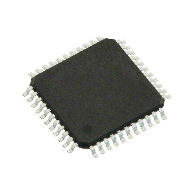
| 描述 | IC CPLD 32MC 7.5NS 44TQFPCPLD - 复杂可编程逻辑器件 CPLD - MAX 3000A 32 Macro 34 IOs |
| 产品分类 | |
| I/O数 | 34 |
| 品牌 | Altera Corporation |
| 产品手册 | |
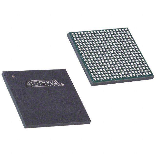
| 产品图片 |
|
| rohs | 符合RoHS无铅 / 符合限制有害物质指令(RoHS)规范要求 |
| 产品系列 | 嵌入式处理器和控制器,CPLD - 复杂可编程逻辑器件,Altera Corporation EPM3032ATC44-7NMAX® 3000A |
| 数据手册 | 点击此处下载产品Datasheethttp://www.altera.com/literature/ds/pkgds.pdf#page=53-54点击此处下载产品Datasheet |
| 产品型号 | EPM3032ATC44-7N |
| PCN设计/规格 | |
| 产品 | MAX 3000A |
| 产品目录页面 | |
| 产品种类 | CPLD - 复杂可编程逻辑器件 |
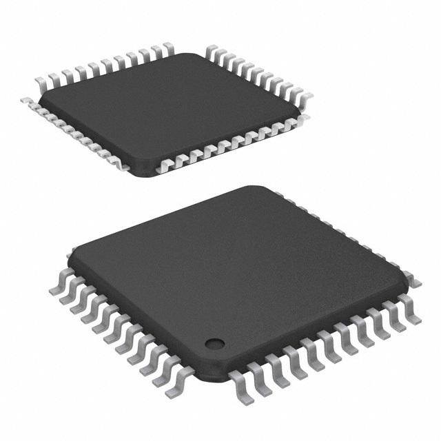
| 供应商器件封装 | 44-TQFP(10x10) |
| 其它名称 | 544-1970 |
| 包装 | 托盘 |
| 可编程类型 | 系统内可编程 |
| 商标 | Altera Corporation |
| 大电池数量 | 32 |
| 存储类型 | EEPROM |
| 安装类型 | 表面贴装 |
| 安装风格 | SMD/SMT |
| 宏单元数 | 32 |
| 封装 | Tray |
| 封装/外壳 | 44-TQFP |
| 封装/箱体 | TQFP-44 |
| 工作温度 | 0°C ~ 85°C |
| 工作电源电压 | 3.3 V |
| 工厂包装数量 | 160 |
| 延迟时间 | 4.5 ns |
| 延迟时间tpd(1)最大值 | 7.5ns |
| 最大工作温度 | + 70 C |
| 最大工作频率 | 227.3 MHz |
| 最小工作温度 | 0 C |
| 栅极数 | 600 |
| 栅极数量 | 600 |
| 标准包装 | 480 |
| 每个宏指令的积项数 | 32 |
| 电源电压-内部 | 3 V ~ 3.6 V |
| 电源电压-最大 | 3.6 V |
| 电源电压-最小 | 3 V |
| 系列 | MAX 3000A |
| 输入/输出端数量 | 34 |
| 逻辑元件/块数 | 2 |
| 逻辑数组块数量——LAB | 2 |


- 商务部:美国ITC正式对集成电路等产品启动337调查
- 曝三星4nm工艺存在良率问题 高通将骁龙8 Gen1或转产台积电
- 太阳诱电将投资9.5亿元在常州建新厂生产MLCC 预计2023年完工
- 英特尔发布欧洲新工厂建设计划 深化IDM 2.0 战略
- 台积电先进制程称霸业界 有大客户加持明年业绩稳了
- 达到5530亿美元!SIA预计今年全球半导体销售额将创下新高
- 英特尔拟将自动驾驶子公司Mobileye上市 估值或超500亿美元
- 三星加码芯片和SET,合并消费电子和移动部门,撤换高东真等 CEO
- 三星电子宣布重大人事变动 还合并消费电子和移动部门
- 海关总署:前11个月进口集成电路产品价值2.52万亿元 增长14.8%


PDF Datasheet 数据手册内容提取
MAX 3000A Programmable Logic ® Device Family June 2006, ver. 3.5 Data Sheet Features... ■ High–performance, low–cost CMOS EEPROM–based programmable logic devices (PLDs) built on a MAX® architecture (see Table1) ■ 3.3-V in-system programmability (ISP) through the built–in IEEE Std. 1149.1 Joint Test Action Group (JTAG) interface with advanced pin-locking capability – ISP circuitry compliant with IEEE Std. 1532 ■ Built–in boundary-scan test (BST) circuitry compliant with IEEE Std. 1149.1-1990 ■ Enhanced ISP features: – Enhanced ISP algorithm for faster programming – ISP_Done bit to ensure complete programming – Pull-up resistor on I/O pins during in–system programming ■ High–density PLDs ranging from 600 to 10,000 usable gates ■ 4.5–ns pin–to–pin logic delays with counter frequencies of up to 227.3MHz ■ MultiVoltTM I/O interface enabling the device core to run at 3.3 V, while I/O pins are compatible with 5.0–V, 3.3–V, and 2.5–V logic levels ■ Pin counts ranging from 44 to 256 in a variety of thin quad flat pack (TQFP), plastic quad flat pack (PQFP), plastic J–lead chip carrier (PLCC), and FineLine BGATM packages ■ Hot–socketing support ■ Programmable interconnect array (PIA) continuous routing structure for fast, predictable performance ■ Industrial temperature range Table 1.MAX3000A Device Features Feature EPM3032A EPM3064A EPM3128A EPM3256A EPM3512A Usable gates 600 1,250 2,500 5,000 10,000 Macrocells 32 64 128 256 512 Logic array blocks 2 4 8 16 32 Maximum user I/O 34 66 98 161 208 pins t (ns) 4.5 4.5 5.0 7.5 7.5 PD t (ns) 2.9 2.8 3.3 5.2 5.6 SU t (ns) 3.0 3.1 3.4 4.8 4.7 CO1 f (MHz) 227.3 222.2 192.3 126.6 116.3 CNT Altera Corporation 1 DS-MAX3000A-3.5
MAX 3000A Programmable Logic Device Family Data Sheet ...and More ■ PCI compatible ■ Bus–friendly architecture including programmable slew–rate control Features ■ Open–drain output option ■ Programmable macrocell flipflops with individual clear, preset, clock, and clock enable controls ■ Programmable power–saving mode for a power reduction of over 50% in each macrocell ■ Configurable expander product–term distribution, allowing up to 32 product terms per macrocell ■ Programmable security bit for protection of proprietary designs ■ Enhanced architectural features, including: – 6 or 10 pin– or logic–driven output enable signals – Two global clock signals with optional inversion – Enhanced interconnect resources for improved routability – Programmable output slew–rate control ■ Software design support and automatic place–and–route provided by Altera’s development systems for Windows–based PCs and Sun SPARCstations, and HP 9000 Series 700/800 workstations ■ Additional design entry and simulation support provided by EDIF 2 0 0 and 3 0 0 netlist files, library of parameterized modules (LPM), Verilog HDL, VHDL, and other interfaces to popular EDA tools from third–party manufacturers such as Cadence, Exemplar Logic, Mentor Graphics, OrCAD, Synopsys, Synplicity, and VeriBest ■ Programming support with the Altera master programming unit (MPU), MasterBlasterTM communications cable, ByteBlasterMVTM parallel port download cable, BitBlasterTM serial download cable as well as programming hardware from third–party manufacturers and any in–circuit tester that supports JamTM Standard Test and Programming Language (STAPL) Files (.jam), Jam STAPL Byte-Code Files (.jbc), or Serial Vector Format Files (.svf) General MAX3000A devices are low–cost, high–performance devices based on the Altera MAX architecture. Fabricated with advanced CMOS technology, Description the EEPROM–based MAX3000A devices operate with a 3.3-V supply voltage and provide 600 to 10,000 usable gates, ISP, pin-to-pin delays as fast as 4.5 ns, and counter speeds of up to 227.3MHz. MAX3000A devices in the –4, –5, –6, –7, and –10 speed grades are compatible with the timing requirements of the PCI Special Interest Group (PCI SIG) PCILocal Bus Specification, Revision2.2. See Table2. 2 Altera Corporation
MAX 3000A Programmable Logic Device Family Data Sheet Table 2.MAX3000A Speed Grades Device Speed Grade –4 –5 –6 –7 –10 EPM3032A v v v EPM3064A v v v EPM3128A v v v EPM3256A v v EPM3512A v v The MAX3000A architecture supports 100% transistor-to-transistor logic (TTL) emulation and high–density small-scale integration (SSI), medium-scale integration (MSI), and large-scale integration (LSI) logic functions. The MAX3000A architecture easily integrates multiple devices ranging from PALs, GALs, and 22V10s to MACH and pLSI devices. MAX3000A devices are available in a wide range of packages, including PLCC, PQFP, and TQFP packages. See Table3. Table 3.MAX3000A Maximum User I/O Pins Note (1) Device 44–Pin 44–Pin 100–Pin 144–Pin 208–Pin 256-Pin PLCC TQFP TQFP TQFP PQFP FineLine BGA EPM3032A 34 34 EPM3064A 34 34 66 EPM3128A 80 96 98 EPM3256A 116 158 161 EPM3512A 172 208 Note: (1) When the IEEE Std. 1149.1 (JTAG) interface is used for in–system programming or boundary–scan testing, four I/O pins become JTAG pins. MAX3000A devices use CMOS EEPROM cells to implement logic functions. The user–configurable MAX3000A architecture accommodates a variety of independent combinatorial and sequential logic functions. The devices can be reprogrammed for quick and efficient iterations during design development and debugging cycles, and can be programmed and erased up to 100 times. Altera Corporation 3
MAX 3000A Programmable Logic Device Family Data Sheet MAX3000A devices contain 32 to 512 macrocells, combined into groups of 16 macrocells called logic array blocks (LABs). Each macrocell has a programmable–AND/fixed–OR array and a configurable register with independently programmable clock, clock enable, clear, and preset functions. To build complex logic functions, each macrocell can be supplemented with shareable expander and high–speed parallel expander product terms to provide up to 32 product terms per macrocell. MAX3000A devices provide programmable speed/power optimization. Speed–critical portions of a design can run at high speed/full power, while the remaining portions run at reduced speed/low power. This speed/power optimization feature enables the designer to configure one or more macrocells to operate at 50% or lower power while adding only a nominal timing delay. MAX3000A devices also provide an option that reduces the slew rate of the output buffers, minimizing noise transients when non–speed–critical signals are switching. The output drivers of all MAX3000A devices can be set for 2.5V or 3.3V, and all input pins are 2.5–V, 3.3–V, and 5.0-V tolerant, allowing MAX3000A devices to be used in mixed–voltage systems. MAX3000A devices are supported by Altera development systems, which are integrated packages that offer schematic, text—including VHDL, Verilog HDL, and the Altera Hardware Description Language (AHDL)—and waveform design entry, compilation and logic synthesis, simulation and timing analysis, and device programming. The software provides EDIF 2 0 0 and 3 0 0, LPM, VHDL, Verilog HDL, and other interfaces for additional design entry and simulation support from other industry–standard PC– and UNIX–workstation–based EDA tools. The software runs on Windows–based PCs, as well as Sun SPARCstation, and HP 9000 Series 700/800 workstations. f For more information on development tools, see the MAX+PLUSII Programmable Logic Development System & Software Data Sheet and the Quartus Programmable Logic Development System & Software Data Sheet. Functional The MAX3000A architecture includes the following elements: Description ■ Logic array blocks (LABs) ■ Macrocells ■ Expander product terms (shareable and parallel) ■ Programmable interconnect array (PIA) ■ I/O control blocks The MAX3000A architecture includes four dedicated inputs that can be used as general–purpose inputs or as high–speed, global control signals (clock, clear, and two output enable signals) for each macrocell and I/O pin. Figure1 shows the architecture of MAX3000A devices. 4 Altera Corporation
MAX 3000A Programmable Logic Device Family Data Sheet Figure 1. MAX3000A Device Block Diagram INPUT/GCLK1 INPUT/OE2/GCLK2 INPUT/OE1 INPUT/GCLRn 6 or 10 Output Enables (1) 6 or 10 Output Enables (1) LAB A LAB B 2 to 2 to I/O 16 Macrocells 36 36 Macrocells 16 I/O 2 to 16 I/O Control 1 to 16 17 to 32 Control 2 to 16 I/O Block Block 16 16 6 or 10 2 to 16 2 to 16 6 or 10 LAB C PIA LAB D 2 to 2 to I/O 16 Macrocells 36 36 Macrocells 16 I/O 2 to 16 I/O CBolonctrkol 33 to 48 49 to 64 CBolonctrkol 2 to 16 I/O 16 16 6 or 10 2 to 16 2 to 16 6 or 10 Note: (1) EPM3032A, EPM3064A, EPM3128A, and EPM3256A devices have six output enables. EPM3512A devices have 10output enables. Logic Array Blocks The MAX3000A device architecture is based on the linking of high–performance LABs. LABs consist of 16–macrocell arrays, as shown in Figure1. Multiple LABs are linked together via the PIA, a global bus that is fed by all dedicated input pins, I/O pins, and macrocells. Each LAB is fed by the following signals: ■ 36 signals from the PIA that are used for general logic inputs ■ Global controls that are used for secondary register functions Altera Corporation 5
MAX 3000A Programmable Logic Device Family Data Sheet Macrocells MAX3000A macrocells can be individually configured for either sequential or combinatorial logic operation. Macrocells consist of three functional blocks: logic array, product–term select matrix, and programmable register. Figure2 shows a MAX3000A macrocell. Figure 2. MAX3000A Macrocell Global Global LAB Local Array Clear Clocks 2 Parallel Logic Expanders Programmable (from other Register macrocells) Register Bypass To I/O Control PRN Block D/T Q Product- Clock/ Term Enable ENA Select Select CLRN Matrix VCC Clear Select To PIA Shared Logic Expanders 36 Signals 16 Expander from PIA Product Terms Combinatorial logic is implemented in the logic array, which provides five product terms per macrocell. The product–term select matrix allocates these product terms for use as either primary logic inputs (to the OR and XOR gates) to implement combinatorial functions, or as secondary inputs to the macrocell’s register preset, clock, and clock enable control functions. Two kinds of expander product terms (“expanders”) are available to supplement macrocell logic resources: ■ Shareable expanders, which are inverted product terms that are fed back into the logic array ■ Parallel expanders, which are product terms borrowed from adjacent macrocells The Altera development system automatically optimizes product–term allocation according to the logic requirements of the design. 6 Altera Corporation
MAX 3000A Programmable Logic Device Family Data Sheet For registered functions, each macrocell flipflop can be individually programmed to implement D, T, JK, or SR operation with programmable clock control. The flipflop can be bypassed for combinatorial operation. During design entry, the designer specifies the desired flipflop type; the Altera development system software then selects the most efficient flipflop operation for each registered function to optimize resource utilization. Each programmable register can be clocked in three different modes: ■ Global clock signal mode, which achieves the fastest clock–to–output performance. ■ Global clock signal enabled by an active–high clock enable. A clock enable is generated by a product term. This mode provides an enable on each flipflop while still achieving the fast clock–to–output performance of the global clock. ■ Array clock implemented with a product term. In this mode, the flipflop can be clocked by signals from buried macrocells or I/O pins. Two global clock signals are available in MAX3000A devices. As shown in Figure1, these global clock signals can be the true or the complement of either of the two global clock pins, GCLK1 or GCLK2. Each register also supports asynchronous preset and clear functions. As shown in Figure2, the product–term select matrix allocates product terms to control these operations. Although the product–term–driven preset and clear from the register are active high, active–low control can be obtained by inverting the signal within the logic array. In addition, each register clear function can be individually driven by the active–low dedicated global clear pin (GCLRn). All registers are cleared upon power-up. By default, all registered outputs drive low when the device is powered up. You can set the registered outputs to drive high upon power-up through the Quartus®II software. Quartus II software uses the NOT Gate Push-Back method, which uses an additional macrocell to set the output high. To set this in the Quartus II software, go to the Assignment Editor and set the Power-Up Level assignment for the register to High. Altera Corporation 7
MAX 3000A Programmable Logic Device Family Data Sheet Expander Product Terms Although most logic functions can be implemented with the five product terms available in each macrocell, highly complex logic functions require additional product terms. Another macrocell can be used to supply the required logic resources. However, the MAX3000A architecture also offers both shareable and parallel expander product terms (“expanders”) that provide additional product terms directly to any macrocell in the same LAB. These expanders help ensure that logic is synthesized with the fewest possible logic resources to obtain the fastest possible speed. Shareable Expanders Each LAB has 16 shareable expanders that can be viewed as a pool of uncommitted single product terms (one from each macrocell) with inverted outputs that feed back into the logic array. Each shareable expander can be used and shared by any or all macrocells in the LAB to build complex logic functions. Shareable expanders incur a small delay (t ). Figure3 shows how shareable expanders can feed multiple SEXP macrocells. Figure 3. MAX3000A Shareable Expanders Shareable expanders can be shared by any or all macrocells in an LAB. Macrocell Product-Term Logic Product-Term Select Matrix Macrocell Product-Term Logic 36 Signals 16 Shared from PIA Expanders 8 Altera Corporation
MAX 3000A Programmable Logic Device Family Data Sheet Parallel Expanders Parallel expanders are unused product terms that can be allocated to a neighboring macrocell to implement fast, complex logic functions. Parallel expanders allow up to 20 product terms to directly feed the macrocell OR logic, with five product terms provided by the macrocell and 15 parallel expanders provided by neighboring macrocells in the LAB. The Altera development system compiler can automatically allocate up to three sets of up to five parallel expanders to the macrocells that require additional product terms. Each set of five parallel expanders incurs a small, incremental timing delay (t ). For example, if a macrocell PEXP requires 14product terms, the compiler uses the five dedicated product terms within the macrocell and allocates two sets of parallel expanders; the first set includes five product terms, and the second set includes four product terms, increasing the total delay by 2 × t . PEXP Two groups of eight macrocells within each LAB (e.g., macrocells 1 through 8 and 9through 16) form two chains to lend or borrow parallel expanders. A macrocell borrows parallel expanders from lower– numbered macrocells. For example, macrocell 8 can borrow parallel expanders from macrocell 7, from macrocells 7 and 6, or from macrocells 7, 6, and 5. Within each group of eight, the lowest–numbered macrocell can only lend parallel expanders and the highest–numbered macrocell can only borrow them. Figure4 shows how parallel expanders can be borrowed from a neighboring macrocell. Altera Corporation 9
MAX 3000A Programmable Logic Device Family Data Sheet Figure 4. MAX3000A Parallel Expanders Unused product terms in a macrocell can be allocated to a neighboring macrocell. From Previous Macrocell Preset Product- Macrocell er Select Product- Matrix Term Logic Clock Clear Preset Product- Macrocell TTTerm Product- Select Term Logic Matrix Clock Clear To Next Macrocell 36 Signals 16 Shared from PIA Expanders Programmable Interconnect Array Logic is routed between LABs on the PIA. This global bus is a programmable path that connects any signal source to any destination on the device. All MAX3000A dedicated inputs, I/O pins, and macrocell outputs feed the PIA, which makes the signals available throughout the entire device. Only the signals required by each LAB are actually routed from the PIA into the LAB. Figure5 shows how the PIA signals are routed into the LAB. An EEPROM cell controls one input to a two-input AND gate, which selects a PIA signal to drive into the LAB. 10 Altera Corporation
MAX 3000A Programmable Logic Device Family Data Sheet Figure 5. MAX3000A PIA Routing To LAB PIA Signals While the routing delays of channel–based routing schemes in masked or FPGAs are cumulative, variable, and path–dependent, the MAX3000A PIA has a predictable delay. The PIA makes a design’s timing performance easy to predict. I/O Control Blocks The I/O control block allows each I/O pin to be individually configured for input, output, or bidirectional operation. All I/O pins have a tri–state buffer that is individually controlled by one of the global output enable signals or directly connected to ground or V . Figure6 shows the I/O CC control block for MAX3000A devices. The I/O control block has 6 or 10global output enable signals that are driven by the true or complement of two output enable signals, a subset of the I/O pins, or a subset of the I/O macrocells. Altera Corporation 11
MAX 3000A Programmable Logic Device Family Data Sheet Figure 6. I/O Control Block of MAX3000A Devices 6 or 10 Global Output Enable Signals (1) PIA OE Select Multiplexer VCC to Other I/O Pins from GND Macrocell Open-Drain Output Slew-Rate Control to PIA Note: (1) EPM3032A, EPM3064A, EPM3128A, and EPM3256A devices have six output enables. EPM3512A devices have 10output enables. When the tri–state buffer control is connected to ground, the output is tri-stated (high impedance), and the I/O pin can be used as a dedicated input. When the tri–state buffer control is connected to V , the output is CC enabled. The MAX3000A architecture provides dual I/O feedback, in which macrocell and pin feedbacks are independent. When an I/O pin is configured as an input, the associated macrocell can be used for buried logic. 12 Altera Corporation
MAX 3000A Programmable Logic Device Family Data Sheet In–System MAX3000A devices can be programmed in–system via an industry– standard four–pin IEEE Std. 1149.1-1990 (JTAG) interface. In-system Programma- programmability (ISP) offers quick, efficient iterations during design bility development and debugging cycles. The MAX3000A architecture internally generates the high programming voltages required to program its EEPROM cells, allowing in–system programming with only a single 3.3–V power supply. During in–system programming, the I/O pins are tri–stated and weakly pulled–up to eliminate board conflicts. The pull–up value is nominally 50 kΩ. MAX3000A devices have an enhanced ISP algorithm for faster programming. These devices also offer an ISP_Done bit that ensures safe operation when in–system programming is interrupted. This ISP_Done bit, which is the last bit programmed, prevents all I/O pins from driving until the bit is programmed. ISP simplifies the manufacturing flow by allowing devices to be mounted on a printed circuit board (PCB) with standard pick–and–place equipment before they are programmed. MAX3000A devices can be programmed by downloading the information via in–circuit testers, embedded processors, the MasterBlaster communications cable, the ByteBlasterMV parallel port download cable, and the BitBlaster serial download cable. Programming the devices after they are placed on the board eliminates lead damage on high–pin–count packages (e.g., QFP packages) due to device handling. MAX3000A devices can be reprogrammed after a system has already shipped to the field. For example, product upgrades can be performed in the field via software or modem. The Jam STAPL programming and test language can be used to program MAX3000A devices with in–circuit testers, PCs, or embedded processors. f For more information on using the Jam STAPL programming and test language, see Application Note 88 (Using the Jam Language for ISP & ICR via an Embedded Processor), Application Note 122 (Using Jam STAPL for ISP & ICR via an Embedded Processor) and AN 111 (Embedded Programming Using the 8051 and Jam Byte-Code). The ISP circuitry in MAX3000A devices is compliant with the IEEE Std. 1532 specification. The IEEE Std. 1532 is a standard developed to allow concurrent ISP between multiple PLD vendors. Altera Corporation 13
MAX 3000A Programmable Logic Device Family Data Sheet Programming Sequence During in-system programming, instructions, addresses, and data are shifted into the MAX 3000A device through the TDI input pin. Data is shifted out through the TDO output pin and compared against the expected data. Programming a pattern into the device requires the following six ISP stages. A stand-alone verification of a programmed pattern involves only stages 1, 2, 5, and 6. 1. Enter ISP. The enter ISP stage ensures that the I/O pins transition smoothly from user mode to ISP mode. The enter ISP stage requires 1ms. 2. Check ID. Before any program or verify process, the silicon ID is checked. The time required to read this silicon ID is relatively small compared to the overall programming time. 3. Bulk Erase. Erasing the device in-system involves shifting in the instructions to erase the device and applying one erase pulse of 100ms. 4. Program. Programming the device in-system involves shifting in the address and data and then applying the programming pulse to program the EEPROM cells. This process is repeated for each EEPROM address. 5. Verify. Verifying an Altera device in-system involves shifting in addresses, applying the read pulse to verify the EEPROM cells, and shifting out the data for comparison. This process is repeated for each EEPROM address. 6. Exit ISP. An exit ISP stage ensures that the I/O pins transition smoothly from ISP mode to user mode. The exit ISP stage requires 1ms. Programming Times The time required to implement each of the six programming stages can be broken into the following two elements: ■ A pulse time to erase, program, or read the EEPROM cells. ■ A shifting time based on the test clock (TCK) frequency and the number of TCK cycles to shift instructions, address, and data into the device. 14 Altera Corporation
MAX 3000A Programmable Logic Device Family Data Sheet By combining the pulse and shift times for each of the programming stages, the program or verify time can be derived as a function of the TCK frequency, the number of devices, and specific target device(s). Because different ISP-capable devices have a different number of EEPROM cells, both the total fixed and total variable times are unique for a single device. Programming a Single MAX 3000A Device The time required to program a single MAX 3000A device in-system can be calculated from the following formula: Cycle PTCK t = t +-------------------------------- PROG PPULSE f TCK where: t = Programming time PROG t = Sum of the fixed times to erase, program, and PPULSE verify the EEPROM cells Cycle = Number of TCK cycles to program a device PTCK f = TCK frequency TCK The ISP times for a stand-alone verification of a single MAX 3000A device can be calculated from the following formula: Cycle VTCK t = t +-------------------------------- VER VPULSE f TCK where: t = Verify time VER t = Sum of the fixed times to verify the EEPROM cells VPULSE Cycle = Number of TCK cycles to verify a device VTCK Altera Corporation 15
MAX 3000A Programmable Logic Device Family Data Sheet The programming times described in Tables4 through 6 are associated with the worst-case method using the enhanced ISP algorithm. Table 4.MAX 3000A t & Cycle Values PULSE TCK Device Programming Stand-Alone Verification t (s) Cycle t (s) Cycle PPULSE PTCK VPULSE VTCK EPM3032A 2.00 55,000 0.002 18,000 EPM3064A 2.00 105,000 0.002 35,000 EPM3128A 2.00 205,000 0.002 68,000 EPM3256A 2.00 447,000 0.002 149,000 EPM3512A 2.00 890,000 0.002 297,000 Tables5 and 6 show the in-system programming and stand alone verification times for several common test clock frequencies. Table 5.MAX 3000A In-System Programming Times for Different Test Clock Frequencies Device f Units TCK 10 MHz 5 MHz 2 MHz 1 MHz 500 kHz 200 kHz 100 kHz 50 kHz EPM3032A 2.01 2.01 2.03 2.06 2.11 2.28 2.55 3.10 s EPM3064A 2.01 2.02 2.05 2.11 2.21 2.53 3.05 4.10 s EPM3128A 2.02 2.04 2.10 2.21 2.41 3.03 4.05 6.10 s EPM3256A 2.05 2.09 2.23 2.45 2.90 4.24 6.47 10.94 s EPM3512A 2.09 2.18 2.45 2.89 3.78 6.45 10.90 19.80 s Table 6.MAX 3000A Stand-Alone Verification Times for Different Test Clock Frequencies Device f Units TCK 10 MHz 5 MHz 2 MHz 1 MHz 500 kHz 200 kHz 100 kHz 50 kHz EPM3032A 0.00 0.01 0.01 0.02 0.04 0.09 0.18 0.36 s EPM3064A 0.01 0.01 0.02 0.04 0.07 0.18 0.35 0.70 s EPM3128A 0.01 0.02 0.04 0.07 0.14 0.34 0.68 1.36 s EPM3256A 0.02 0.03 0.08 0.15 0.30 0.75 1.49 2.98 s EPM3512A 0.03 0.06 0.15 0.30 0.60 1.49 2.97 5.94 s 16 Altera Corporation
MAX 3000A Programmable Logic Device Family Data Sheet Programming MAX3000A devices can be programmed on Windows–based PCs with an Altera Logic Programmer card, MPU, and the appropriate device adapter. with External The MPU performs continuity checking to ensure adequate electrical Hardware contact between the adapter and the device. f For more information, see the Altera Programming Hardware Data Sheet. The Altera software can use text– or waveform–format test vectors created with the Altera Text Editor or Waveform Editor to test the programmed device. For added design verification, designers can perform functional testing to compare the functional device behavior with the results of simulation. Data I/O, BP Microsystems, and other programming hardware manufacturers also provide programming support for Altera devices. f For more information, see Programming Hardware Manufacturers. IEEE Std. MAX3000A devices include the JTAG BST circuitry defined by IEEE Std.1149.1–1990. Table7 describes the JTAG instructions supported by 1149.1 (JTAG) MAX3000A devices. The pin-out tables found on the Altera web site Boundary–Scan (http://www.altera.com) or the Altera Digital Library show the location of the JTAG control pins for each device. If the JTAG interface is not Support required, the JTAG pins are available as user I/O pins. Table 7.MAX3000A JTAG Instructions JTAG Instruction Description SAMPLE/PRELOAD Allows a snapshot of signals at the device pins to be captured and examined during normal device operation, and permits an initial data pattern output at the device pins EXTEST Allows the external circuitry and board–level interconnections to be tested by forcing a test pattern at the output pins and capturing test results at the input pins BYPASS Places the 1–bit bypass register between the TDI and TDO pins, which allows the BST data to pass synchronously through a selected device to adjacent devices during normal device operation IDCODE Selects the IDCODE register and places it between the TDI and TDO pins, allowing the IDCODE to be serially shifted out of TDO USERCODE Selects the 32–bit USERCODE register and places it between the TDI and TDO pins, allowing the USERCODE value to be shifted out of TDO ISP Instructions These instructions are used when programming MAX3000A devices via the JTAG ports with the MasterBlaster, ByteBlasterMV, or BitBlaster cable, or when using a Jam STAPL file, JBC file, or SVF file via an embedded processor or test equipment Altera Corporation 17
MAX 3000A Programmable Logic Device Family Data Sheet The instruction register length of MAX3000A devices is 10 bits. The IDCODE and USERCODE register length is 32 bits. Tables8 and 9 show the boundary–scan register length and device IDCODE information for MAX3000A devices. Table 8.MAX3000A Boundary–Scan Register Length Device Boundary–Scan Register Length EPM3032A 96 EPM3064A 192 EPM3128A 288 EPM3256A 480 EPM3512A 624 Table 9.32–Bit MAX3000A Device IDCODE Value Note (1) Device IDCODE (32 bits) Version Part Number (16 Bits) Manufacturer’s 1 (1 Bit) (4 Bits) Identity (11 Bits) (2) EPM3032A 0001 0111 0000 0011 0010 00001101110 1 EPM3064A 0001 0111 0000 0110 0100 00001101110 1 EPM3128A 0001 0111 0001 0010 1000 00001101110 1 EPM3256A 0001 0111 0010 0101 0110 00001101110 1 EPM3512A 0001 0111 0101 0001 0010 00001101110 1 Notes: (1) The most significant bit (MSB) is on the left. (2) The least significant bit (LSB) for all JTAG IDCODEs is 1. f See Application Note 39 (IEEE 1149.1 (JTAG) Boundary–Scan Testing in Altera Devices) for more information on JTAG BST. 18 Altera Corporation
MAX 3000A Programmable Logic Device Family Data Sheet Figure7 shows the timing information for the JTAG signals. Figure 7. MAX3000A JTAG Waveforms TMS TDI tJCP tJCH tJCL tJPSU tJPH TCK tJPZX tJPCO tJPXZ TDO t t JSSU JSH Signal to Be Captured tJSZX tJSCO tJSXZ Signal to Be Driven Table10 shows the JTAG timing parameters and values for MAX3000A devices. Table 10.JTAG Timing Parameters & Values for MAX3000A Devices Symbol Parameter Min Max Unit tJCP TCK clock period 100 ns tJCH TCK clock high time 50 ns tJCL TCK clock low time 50 ns tJPSU JTAG port setup time 20 ns tJPH JTAG port hold time 45 ns tJPCO JTAG port clock to output 25 ns tJPZX JTAG port high impedance to valid output 25 ns tJPXZ JTAG port valid output to high impedance 25 ns tJSSU Capture register setup time 20 ns tJSH Capture register hold time 45 ns tJSCO Update register clock to output 25 ns tJSZX Update register high impedance to valid output 25 ns tJSXZ Update register valid output to high impedance 25 ns Altera Corporation 19
MAX 3000A Programmable Logic Device Family Data Sheet Programmable MAX3000A devices offer a power–saving mode that supports low-power operation across user–defined signal paths or the entire device. This Speed/Power feature allows total power dissipation to be reduced by 50% or more Control because most logic applications require only a small fraction of all gates to operate at maximum frequency. The designer can program each individual macrocell in a MAX3000A device for either high–speed or low–power operation. As a result, speed-critical paths in the design can run at high speed, while the remaining paths can operate at reduced power. Macrocells that run at low power incur a nominal timing delay adder (t ) for the t , t , t , LPA LAD LAC IC t , t , t and t parameters. ACL EN CPPW SEXP Output MAX3000A device outputs can be programmed to meet a variety of system–level requirements. Configuration MultiVolt I/O Interface The MAX3000A device architecture supports the MultiVolt I/O interface feature, which allows MAX3000A devices to connect to systems with differing supply voltages. MAX3000A devices in all packages can be set for 2.5–V, 3.3–V, or 5.0–V I/O pin operation. These devices have one set of V pins for internal operation and input buffers (VCCINT), and another CC set for I/O output drivers (VCCIO). The VCCIO pins can be connected to either a 3.3–V or 2.5–V power supply, depending on the output requirements. When the VCCIO pins are connected to a 2.5–V power supply, the output levels are compatible with 2.5–V systems. When the VCCIO pins are connected to a 3.3–V power supply, the output high is at 3.3V and is therefore compatible with 3.3-V or 5.0–V systems. Devices operating with V levels lower than 3.0V CCIO incur a nominally greater timing delay of t instead of t . Inputs can OD2 OD1 always be driven by 2.5–V, 3.3–V, or 5.0–V signals. Table11 summarizes the MAX3000A MultiVolt I/O support. Table 11.MAX3000A MultiVolt I/O Support V Voltage Input Signal (V) Output Signal (V) CCIO 2.5 3.3 5.0 2.5 3.3 5.0 2.5 v v v v 3.3 v v v v v v Note: (1) When VCCIO is 3.3 V, a MAX 3000A device can drive a 2.5–V device that has 3.3–V tolerant inputs. 20 Altera Corporation
MAX 3000A Programmable Logic Device Family Data Sheet Open–Drain Output Option MAX3000A devices provide an optional open–drain (equivalent to open-collector) output for each I/O pin. This open–drain output enables the device to provide system–level control signals (e.g., interrupt and write enable signals) that can be asserted by any of several devices. It can also provide an additional wired–OR plane. Open-drain output pins on MAX3000A devices (with a pull-up resistor to the 5.0-V supply) can drive 5.0-V CMOS input pins that require a high V . IH When the open-drain pin is active, it will drive low. When the pin is inactive, the resistor will pull up the trace to 5.0V, thereby meeting CMOS requirements. The open-drain pin will only drive low or tri-state; it will never drive high. The rise time is dependent on the value of the pull-up resistor and load impedance. The I current specification should be OL considered when selecting a pull-up resistor Slew–Rate Control The output buffer for each MAX3000A I/O pin has an adjustable output slew rate that can be configured for low–noise or high–speed performance. A faster slew rate provides high–speed transitions for high-performance systems. However, these fast transitions may introduce noise transients into the system. A slow slew rate reduces system noise, but adds a nominal delay of 4 to 5 ns. When the configuration cell is turned off, the slew rate is set for low–noise performance. Each I/O pin has an individual EEPROM bit that controls the slew rate, allowing designers to specify the slew rate on a pin–by–pin basis. The slew rate control affects both the rising and falling edges of the output signal. Design Security All MAX3000A devices contain a programmable security bit that controls access to the data programmed into the device. When this bit is programmed, a design implemented in the device cannot be copied or retrieved. This feature provides a high level of design security because programmed data within EEPROM cells is invisible. The security bit that controls this function, as well as all other programmed data, is reset only when the device is reprogrammed. Generic Testing MAX3000A devices are fully tested. Complete testing of each programmable EEPROM bit and all internal logic elements ensures 100% programming yield. AC test measurements are taken under conditions equivalent to those shown in Figure8. Test patterns can be used and then erased during early stages of the production flow. Altera Corporation 21
MAX 3000A Programmable Logic Device Family Data Sheet Figure 8. MAX3000A AC Test Conditions Power supply transients can affect AC measurements. Simultaneous transitions VCC of multiple outputs should be avoided for accurate measurement. Threshold tests 703 Ω must not be performed under AC [521 Ω] conditions. Large–amplitude, fast– Device To Test ground–current transients normally occur Output System as the device outputs discharge the load capacitances. When these transients flow through the parasitic inductance between 620 Ω the device ground pin and the test system [481 Ω] C1 (includes jig ground, significant reductions in capacitance) observable noise immunity can result. Device input Numbers in brackets are for 2.5–V rise and fall times < 2 ns outputs. Numbers without brackets are for 3.3–V devices or outputs. Operating Tables12 through 15 provide information on absolute maximum ratings, recommended operating conditions, DC operating conditions, and Conditions capacitance for MAX3000A devices. Table 12.MAX3000A Device Absolute Maximum Ratings Note (1) Symbol Parameter Conditions Min Max Unit VCC Supply voltage With respect to ground (2) –0.5 4.6 V VI DC input voltage –2.0 5.75 V IOUT DC output current, per pin –25 25 mA TSTG Storage temperature No bias –65 150 ° C TA Ambient temperature Under bias –65 135 ° C TJ Junction temperature PQFP and TQFP packages, under bias 135 ° C 22 Altera Corporation
MAX 3000A Programmable Logic Device Family Data Sheet Table 13.MAX3000A Device Recommended Operating Conditions Symbol Parameter Conditions Min Max Unit VCCINT Supply voltage for internal logic and (10) 3.0 3.6 V input buffers VCCIO Supply voltage for output drivers, 3.0 3.6 V 3.3–V operation Supply voltage for output drivers, 2.3 2.7 V 2.5–V operation VCCISP Supply voltage during ISP 3.0 3.6 V VI Input voltage (3) –0.5 5.75 V VO Output voltage 0 VCCIO V TA Ambient temperature Commercial range 0 70 ° C Industrial range –40 85 ° C TJ Junction temperature Commercial range 0 90 ° C Industrial range (11) –40 105 ° C tR Input rise time 40 ns tF Input fall time 40 ns Table 14.MAX3000A Device DC Operating Conditions Note (4) Symbol Parameter Conditions Min Max Unit VIH High–level input voltage 1.7 5.75 V VIL Low–level input voltage –0.5 0.8 V VOH 3.3–V high–level TTL output IOH = –8 mA DC, VCCIO = 3.00 V (5) 2.4 V voltage 3.3–V high–level CMOS output IOH = –0.1 mA DC, VCCIO = 3.00 V (5) VCCIO – 0.2 V voltage 2.5–V high–level output voltage IOH = –100 µA DC, VCCIO = 2.30 V (5) 2.1 V IOH = –1 mA DC, VCCIO = 2.30 V (5) 2.0 V IOH = –2 mA DC, VCCIO = 2.30 V (5) 1.7 V VOL 3.3–V low–level TTL output voltage IOL = 8 mA DC, VCCIO = 3.00 V (6) 0.4 V 3.3–V low–level CMOS output IOL = 0.1 mA DC, VCCIO = 3.00 V (6) 0.2 V voltage 2.5–V low–level output voltage IOL = 100 µA DC, VCCIO = 2.30 V (6) 0.2 V IOL = 1 mA DC, VCCIO = 2.30 V (6) 0.4 V IOL = 2 mA DC, VCCIO = 2.30 V (6) 0.7 V II Input leakage current VI = –0.5 to 5.5 V (7) –10 10 μA IOZ Tri–state output off–state current VI = –0.5 to 5.5 V (7) –10 10 μA RISP Value of I/O pin pull–up resistor VCCIO = 2.3 to 3.6 V (8) 20 74 kΩ when programming in–system or during power–up Altera Corporation 23
MAX 3000A Programmable Logic Device Family Data Sheet Table 15.MAX3000A Device Capacitance Note (9) Symbol Parameter Conditions Min Max Unit CIN Input pin capacitance VIN = 0 V, f = 1.0 MHz 8 pF CI/O I/O pin capacitance VOUT = 0 V, f = 1.0 MHz 8 pF Notes to tables: (1) See the Operating Requirements for Altera Devices Data Sheet. (2) Minimum DC input voltage is –0.5 V. During transitions, the inputs may undershoot to –2.0 V or overshoot to 5.75 V for input currents less than 100 mA and periods shorter than 20 ns. (3) All pins, including dedicated inputs, I/O pins, and JTAG pins, may be driven before VCCINT and VCCIO are powered. (4) These values are specified under the recommended operating conditions, as shown in Table13 on page23. (5) The parameter is measured with 50% of the outputs each sourcing the specified current. The IOH parameter refers to high–level TTL or CMOS output current. (6) The parameter is measured with 50% of the outputs each sinking the specified current. The IOL parameter refers to low–level TTL, PCI, or CMOS output current. (7) This value is specified during normal device operation. During power-up, the maximum leakage current is μ ±300 A. (8) This pull–up exists while devices are programmed in–system and in unprogrammed devices during power–up. (9) Capacitance is measured at 25° C and is sample–tested only. The OE1 pin (high–voltage pin during programming) has a maximum capacitance of 20 pF. (10) The POR time for all MAX 3000Adevices does not exceed 100μs. The sufficient VCCINT voltage level for POR is 3.0V. The device is fully initialized within the POR time after VCCINT reaches the sufficient POR voltage level. (11) These devices support in-system programming for –40° to 100° C. For in-system programming support between –40° and 0° C, contact Altera Applications. Figure9 shows the typical output drive characteristics of MAX3000A devices. 24 Altera Corporation
MAX 3000A Programmable Logic Device Family Data Sheet Figure 9. Output Drive Characteristics of MAX3000A Devices 3.3 V 150 I OL 100 Typical IO VCCINT = 3.3 V Output V = 3.3 V CCIO Current (mA) Temperature = 25 O C 50 I OH 0 0 1 2 3 4 V Output Voltage (V) O 2.5 V 150 I OL 100 Typical IO VCCINT = 3.3 V Output V = 2.5 V CCIO Current (mA) Temperature = 25 O C 50 I OH 0 0 1 2 3 4 V Output Voltage (V) O Power Because MAX3000A devices can be used in a mixed–voltage environment, they have been designed specifically to tolerate any possible Sequencing & power–up sequence. The V and V power planes can be CCIO CCINT Hot–Socketing powered in any order. Signals can be driven into MAX3000A devices before and during power-up without damaging the device. In addition, MAX3000A devices do not drive out during power-up. Once operating conditions are reached, MAX3000A devices operate as specified by the user. Altera Corporation 25
MAX 3000A Programmable Logic Device Family Data Sheet Timing Model MAX3000A device timing can be analyzed with the Altera software, with a variety of popular industry–standard EDA simulators and timing analyzers, or with the timing model shown in Figure10. MAX3000A devices have predictable internal delays that enable the designer to determine the worst–case timing of any design. The software provides timing simulation, point–to–point delay prediction, and detailed timing analysis for device–wide performance evaluation. Figure 10. MAX3000A Timing Model Internal Output Enable Delay tIOE Input Global Control Delay Delay tIN tGLOB Parallel RDegeilsatyer ODuetlpauyt DtPePIlIAaAy CLooRngDtetttriogLIceLCAA lilA saCDDtryerearlayy ExpantPdEeXrP Delay ttttttSHPCRCURLDOREMB tttttttOOOXZZZZXXXDDD123321 tEN I/O Shared Delay Expander Delay tIO tSEXP The timing characteristics of any signal path can be derived from the timing model and parameters of a particular device. External timing parameters, which represent pin–to–pin timing delays, can be calculated as the sum of internal parameters. Figure11 shows the timing relationship between internal and external delay parameters. 26 Altera Corporation
MAX 3000A Programmable Logic Device Family Data Sheet Figure 11. MAX3000A Switching Waveforms tR & tF < 2 ns. Inputs are Combinatorial Mode driven at 3 V for a logic high and 0 V for a logic tIN low. All timing Input Pin characteristics are tIO measured at 1.5 V. I/O Pin tPIA PIA Delay tSEXP Shared Expander Delay tLAC , tLAD Logic Array Input tPEXP Parallel Expander Delay tCOMB Logic Array Output tOD Output Pin Global Clock Mode Global tR tCH tCL tF Clock Pin tIN Global Clock tGLOB at Register tSU tH Data or Enable (Logic Array Output) Array Clock Mode tR tACH tACL tF Input or I/O Pin tIN tIO Clock into PIA Clock into tPIA Logic Array Clock at tIC Register tSU tH Data from Logic Array tRD tPIA tCLR , tPRE tPIA Register to PIA to Logic Array tOD tOD Register Output to Pin Altera Corporation 27
MAX 3000A Programmable Logic Device Family Data Sheet Tables16 through 23 show EPM3032A, EPM3064A, EPM3128A, EPM3256A, and EPM3512A timing information. Table 16.EPM3032A External Timing Parameters Note (1) Symbol Parameter Conditions Speed Grade Unit –4 –7 –10 Min Max Min Max Min Max t Input to non– C1 = 35 pF 4.5 7.5 10 ns PD1 registered output (2) t I/O input to non– C1 = 35 pF 4.5 7.5 10 ns PD2 registered output (2) t Global clock setup (2) 2.9 4.7 6.3 ns SU time t Global clock hold time (2) 0.0 0.0 0.0 ns H t Global clock to output C1 = 35 pF 1.0 3.0 1.0 5.0 1.0 6.7 ns CO1 delay t Global clock high time 2.0 3.0 4.0 ns CH t Global clock low time 2.0 3.0 4.0 ns CL t Array clock setup time (2) 1.6 2.5 3.6 ns ASU t Array clock hold time (2) 0.3 0.5 0.5 ns AH t Array clock to output C1 = 35 pF 1.0 4.3 1.0 7.2 1.0 9.4 ns ACO1 delay (2) t Array clock high time 2.0 3.0 4.0 ns ACH t Array clock low time 2.0 3.0 4.0 ns ACL t Minimum pulse width (3) 2.0 3.0 4.0 ns CPPW for clear and preset t Minimum global clock (2) 4.4 7.2 9.7 ns CNT period f Maximum internal (2), (4) 227.3 138.9 103.1 MHz CNT global clock frequency t Minimum array clock (2) 4.4 7.2 9.7 ns ACNT period f Maximum internal (2), (4) 227.3 138.9 103.1 MHz ACNT array clock frequency 28 Altera Corporation
MAX 3000A Programmable Logic Device Family Data Sheet Table 17.EPM3032A Internal Timing Parameters (Part 1 of 2) Note (1) Symbol Parameter Conditions Speed Grade Unit –4 –7 –10 Min Max Min Max Min Max t Input pad and buffer delay 0.7 1.2 1.5 ns IN t I/O input pad and buffer 0.7 1.2 1.5 ns IO delay t Shared expander delay 1.9 3.1 4.0 ns SEXP t Parallel expander delay 0.5 0.8 1.0 ns PEXP t Logic array delay 1.5 2.5 3.3 ns LAD t Logic control array delay 0.6 1.0 1.2 ns LAC t Internal output enable delay 0.0 0.0 0.0 ns IOE t Output buffer and pad C1 = 35 pF 0.8 1.3 1.8 ns OD1 delay, slow slew rate = off V = 3.3 V CCIO t Output buffer and pad C1 = 35 pF 1.3 1.8 2.3 ns OD2 delay, slow slew rate=off V = 2.5 V CCIO t Output buffer and pad C1 = 35 pF 5.8 6.3 6.8 ns OD3 delay, slow slew rate = on V = 2.5 V or 3.3 V CCIO t Output buffer enable delay, C1 = 35 pF 4.0 4.0 5.0 ns ZX1 slow slew rate = off V = 3.3 V CCIO t Output buffer enable delay, C1 = 35 pF 4.5 4.5 5.5 ns ZX2 slow slew rate = off V = 2.5 V CCIO t Output buffer enable delay, C1 = 35 pF 9.0 9.0 10.0 ns ZX3 slow slew rate = on V = 2.5 V or 3.3 V CCIO t Output buffer disable delay C1 = 5 pF 4.0 4.0 5.0 ns XZ t Register setup time 1.3 2.0 2.8 ns SU t Register hold time 0.6 1.0 1.3 ns H t Register delay 0.7 1.2 1.5 ns RD t Combinatorial delay 0.6 1.0 1.3 ns COMB t Array clock delay 1.2 2.0 2.5 ns IC t Register enable time 0.6 1.0 1.2 ns EN t Global control delay 0.8 1.3 1.9 ns GLOB t Register preset time 1.2 1.9 2.6 ns PRE t Register clear time 1.2 1.9 2.6 ns CLR Altera Corporation 29
MAX 3000A Programmable Logic Device Family Data Sheet Table 17.EPM3032A Internal Timing Parameters (Part 2 of 2) Note (1) Symbol Parameter Conditions Speed Grade Unit –4 –7 –10 Min Max Min Max Min Max t PIA delay (2) 0.9 1.5 2.1 ns PIA t Low–power adder (5) 2.5 4.0 5.0 ns LPA Table 18.EPM3064A External Timing Parameters Note (1) Symbol Parameter Conditions Speed Grade Unit –4 –7 –10 Min Max Min Max Min Max t Input to non–registered C1 = 35 pF (2) 4.5 7.5 10.0 ns PD1 output t I/O input to non–registered C1 = 35 pF (2) 4.5 7.5 10.0 ns PD2 output t Global clock setup time (2) 2.8 4.7 6.2 ns SU t Global clock hold time (2) 0.0 0.0 0.0 ns H t Global clock to output delay C1 = 35 pF 1.0 3.1 1.0 5.1 1.0 7.0 ns CO1 t Global clock high time 2.0 3.0 4.0 ns CH t Global clock low time 2.0 3.0 4.0 ns CL t Array clock setup time (2) 1.6 2.6 3.6 ns ASU t Array clock hold time (2) 0.3 0.4 0.6 ns AH t Array clock to output delay C1 = 35 pF (2) 1.0 4.3 1.0 7.2 1.0 9.6 ns ACO1 t Array clock high time 2.0 3.0 4.0 ns ACH t Array clock low time 2.0 3.0 4.0 ns ACL t Minimum pulse width for (3) 2.0 3.0 4.0 ns CPPW clear and preset t Minimum global clock (2) 4.5 7.4 10.0 ns CNT period f Maximum internal global (2), (4) 222.2 135.1 100.0 MHz CNT clock frequency t Minimum array clock period (2) 4.5 7.4 10.0 ns ACNT f Maximum internal array (2), (4) 222.2 135.1 100.0 MHz ACNT clock frequency 30 Altera Corporation
MAX 3000A Programmable Logic Device Family Data Sheet Table 19.EPM3064A Internal Timing Parameters (Part 1 of 2) Note (1) Symbol Parameter Conditions Speed Grade Unit –4 –7 –10 Min Max Min Max Min Max t Input pad and buffer delay 0.6 1.1 1.4 ns IN t I/O input pad and buffer 0.6 1.1 1.4 ns IO delay t Shared expander delay 1.8 3.0 3.9 ns SEXP t Parallel expander delay 0.4 0.7 0.9 ns PEXP t Logic array delay 1.5 2.5 3.2 ns LAD t Logic control array delay 0.6 1.0 1.2 ns LAC t Internal output enable delay 0.0 0.0 0.0 ns IOE t Output buffer and pad C1 = 35 pF 0.8 1.3 1.8 ns OD1 delay, slow slew rate = off V = 3.3 V CCIO t Output buffer and pad C1 = 35 pF 1.3 1.8 2.3 ns OD2 delay, slow slew rate=off V = 2.5 V CCIO t Output buffer and pad C1 = 35 pF 5.8 6.3 6.8 ns OD3 delay, slow slew rate = on V = 2.5 V or 3.3 V CCIO t Output buffer enable delay, C1 = 35 pF 4.0 4.0 5.0 ns ZX1 slow slew rate = off V = 3.3 V CCIO t Output buffer enable delay, C1 = 35 pF 4.5 4.5 5.5 ns ZX2 slow slew rate = off V = 2.5 V CCIO t Output buffer enable delay, C1 = 35 pF 9.0 9.0 10.0 ns ZX3 slow slew rate = on V = 2.5 V or 3.3 V CCIO t Output buffer disable delay C1 = 5 pF 4.0 4.0 5.0 ns XZ t Register setup time 1.3 2.0 2.9 ns SU t Register hold time 0.6 1.0 1.3 ns H t Register delay 0.7 1.2 1.6 ns RD t Combinatorial delay 0.6 0.9 1.3 ns COMB t Array clock delay 1.2 1.9 2.5 ns IC t Register enable time 0.6 1.0 1.2 ns EN t Global control delay 1.0 1.5 2.2 ns GLOB t Register preset time 1.3 2.1 2.9 ns PRE Altera Corporation 31
MAX 3000A Programmable Logic Device Family Data Sheet Table 19.EPM3064A Internal Timing Parameters (Part 2 of 2) Note (1) Symbol Parameter Conditions Speed Grade Unit –4 –7 –10 Min Max Min Max Min Max t Register clear time 1.3 2.1 2.9 ns CLR t PIA delay (2) 1.0 1.7 2.3 ns PIA t Low–power adder (5) 3.5 4.0 5.0 ns LPA Table 20.EPM3128A External Timing Parameters Note (1) Symbol Parameter Conditions Speed Grade Unit –5 –7 –10 Min Max Min Max Min Max t Input to non– C1 = 35 pF 5.0 7.5 10 ns PD1 registered output (2) t I/O input to non– C1 = 35 pF 5.0 7.5 10 ns PD2 registered output (2) t Global clock setup (2) 3.3 4.9 6.6 ns SU time t Global clock hold time (2) 0.0 0.0 0.0 ns H t Global clock to output C1 = 35 pF 1.0 3.4 1.0 5.0 1.0 6.6 ns CO1 delay t Global clock high time 2.0 3.0 4.0 ns CH t Global clock low time 2.0 3.0 4.0 ns CL t Array clock setup time (2) 1.8 2.8 3.8 ns ASU t Array clock hold time (2) 0.2 0.3 0.4 ns AH t Array clock to output C1 = 35 pF 1.0 4.9 1.0 7.1 1.0 9.4 ns ACO1 delay (2) t Array clock high time 2.0 3.0 4.0 ns ACH t Array clock low time 2.0 3.0 4.0 ns ACL t Minimum pulse width (3) 2.0 3.0 4.0 ns CPPW for clear and preset t Minimum global clock (2) 5.2 7.7 10.2 ns CNT period f Maximum internal (2), (4) 192.3 129.9 98.0 MHz CNT global clock frequency t Minimum array clock (2) 5.2 7.7 10.2 ns ACNT period 32 Altera Corporation
MAX 3000A Programmable Logic Device Family Data Sheet Table 20.EPM3128A External Timing Parameters Note (1) Symbol Parameter Conditions Speed Grade Unit –5 –7 –10 Min Max Min Max Min Max f Maximum internal (2), (4) 192.3 129.9 98.0 MHz ACNT array clock frequency Table 21.EPM3128A Internal Timing Parameters (Part 1 of 2) Note (1) Symbol Parameter Conditions Speed Grade Unit –5 –7 –10 Min Max Min Max Min Max t Input pad and buffer delay 0.7 1.0 1.4 ns IN t I/O input pad and buffer 0.7 1.0 1.4 ns IO delay t Shared expander delay 2.0 2.9 3.8 ns SEXP t Parallel expander delay 0.4 0.7 0.9 ns PEXP t Logic array delay 1.6 2.4 3.1 ns LAD t Logic control array delay 0.7 1.0 1.3 ns LAC t Internal output enable delay 0.0 0.0 0.0 ns IOE t Output buffer and pad C1 = 35 pF 0.8 1.2 1.6 ns OD1 delay, slow slew rate = off V = 3.3 V CCIO t Output buffer and pad C1 = 35 pF 1.3 1.7 2.1 ns OD2 delay, slow slew rate=off V = 2.5 V CCIO t Output buffer and pad C1 = 35 pF 5.8 6.2 6.6 ns OD3 delay, slow slew rate = on V = 2.5 V or 3.3 V CCIO t Output buffer enable delay, C1 = 35 pF 4.0 4.0 5.0 ns ZX1 slow slew rate = off V = 3.3 V CCIO t Output buffer enable delay, C1 = 35 pF 4.5 4.5 5.5 ns ZX2 slow slew rate = off V = 2.5 V CCIO t Output buffer enable delay, C1 = 35 pF 9.0 9.0 10.0 ns ZX3 slow slew rate = on V = 2.5 V or 3.3 V CCIO t Output buffer disable delay C1 = 5 pF 4.0 4.0 5.0 ns XZ Altera Corporation 33
MAX 3000A Programmable Logic Device Family Data Sheet Table 21.EPM3128A Internal Timing Parameters (Part 2 of 2) Note (1) Symbol Parameter Conditions Speed Grade Unit –5 –7 –10 Min Max Min Max Min Max t Register setup time 1.4 2.1 2.9 ns SU t Register hold time 0.6 1.0 1.3 ns H t Register delay 0.8 1.2 1.6 ns RD t Combinatorial delay 0.5 0.9 1.3 ns COMB t Array clock delay 1.2 1.7 2.2 ns IC t Register enable time 0.7 1.0 1.3 ns EN t Global control delay 1.1 1.6 2.0 ns GLOB t Register preset time 1.4 2.0 2.7 ns PRE t Register clear time 1.4 2.0 2.7 ns CLR t PIA delay (2) 1.4 2.0 2.6 ns PIA t Low–power adder (5) 4.0 4.0 5.0 ns LPA Table 22.EPM3256A External Timing Parameters Note (1) Symbol Parameter Conditions Speed Grade Unit –7 –10 Min Max Min Max t Input to non–registered C1 = 35 pF (2) 7.5 10 ns PD1 output t I/O input to non–registered C1 = 35 pF (2) 7.5 10 ns PD2 output t Global clock setup time (2) 5.2 6.9 ns SU t Global clock hold time (2) 0.0 0.0 ns H t Global clock to output C1 = 35 pF 1.0 4.8 1.0 6.4 ns CO1 delay t Global clock high time 3.0 4.0 ns CH t Global clock low time 3.0 4.0 ns CL t Array clock setup time (2) 2.7 3.6 ns ASU t Array clock hold time (2) 0.3 0.5 ns AH t Array clock to output delay C1 = 35 pF (2) 1.0 7.3 1.0 9.7 ns ACO1 t Array clock high time 3.0 4.0 ns ACH t Array clock low time 3.0 4.0 ns ACL t Minimum pulse width for (3) 3.0 4.0 ns CPPW clear and preset 34 Altera Corporation
MAX 3000A Programmable Logic Device Family Data Sheet Table 22.EPM3256A External Timing Parameters Note (1) Symbol Parameter Conditions Speed Grade Unit –7 –10 Min Max Min Max t Minimum global clock (2) 7.9 10.5 ns CNT period f Maximum internal global (2), (4) 126.6 95.2 MHz CNT clock frequency t Minimum array clock (2) 7.9 10.5 ns ACNT period f Maximum internal array (2), (4) 126.6 95.2 MHz ACNT clock frequency Table 23.EPM3256A Internal Timing Parameters (Part 1 of 2) Note (1) Symbol Parameter Conditions Speed Grade Unit –7 –10 Min Max Min Max t Input pad and buffer delay 0.9 1.2 ns IN t I/O input pad and buffer delay 0.9 1.2 ns IO t Shared expander delay 2.8 3.7 ns SEXP t Parallel expander delay 0.5 0.6 ns PEXP t Logic array delay 2.2 2.8 ns LAD t Logic control array delay 1.0 1.3 ns LAC t Internal output enable delay 0.0 0.0 ns IOE t Output buffer and pad delay, C1 = 35 pF 1.2 1.6 ns OD1 slow slew rate = off V = 3.3 V CCIO t Output buffer and pad delay, C1 = 35 pF 1.7 2.1 ns OD2 slow slew rate=off V = 2.5 V CCIO t Output buffer and pad delay, C1 = 35 pF 6.2 6.6 ns OD3 slow slew rate = on V = 2.5 V or 3.3 V CCIO t Output buffer enable delay, slow C1 = 35 pF 4.0 5.0 ns ZX1 slew rate = off V = 3.3 V CCIO t Output buffer enable delay, slow C1 = 35 pF 4.5 5.5 ns ZX2 slew rate = off V = 2.5 V CCIO Altera Corporation 35
MAX 3000A Programmable Logic Device Family Data Sheet Table 23.EPM3256A Internal Timing Parameters (Part 2 of 2) Note (1) Symbol Parameter Conditions Speed Grade Unit –7 –10 Min Max Min Max t Output buffer enable delay, slow C1 = 35 pF 9.0 10.0 ns ZX3 slew rate = on V = 2.5 V or 3.3 V CCIO t Output buffer disable delay C1 = 5 pF 4.0 5.0 ns XZ t Register setup time 2.1 2.9 ns SU t Register hold time 0.9 1.2 ns H t Register delay 1.2 1.6 ns RD t Combinatorial delay 0.8 1.2 ns COMB t Array clock delay 1.6 2.1 ns IC t Register enable time 1.0 1.3 ns EN t Global control delay 1.5 2.0 ns GLOB t Register preset time 2.3 3.0 ns PRE t Register clear time 2.3 3.0 ns CLR t PIA delay (2) 2.4 3.2 ns PIA t Low–power adder (5) 4.0 5.0 ns LPA Table 24.EPM3512A External Timing Parameters Note (1) Symbol Parameter Conditions Speed Grade Unit -7 -10 Min Max Min Max t Input to non-registered output C1 = 35 pF (2) 7.5 10.0 ns PD1 t I/O input to non-registered C1 = 35 pF (2) 7.5 10.0 ns PD2 output t Global clock setup time (2) 5.6 7.6 ns SU t Global clock hold time (2) 0.0 0.0 ns H t Global clock setup time of fast 3.0 3.0 ns FSU input t Global clock hold time of fast 0.0 0.0 ns FH input t Global clock to output delay C1 = 35 pF 1.0 4.7 1.0 6.3 ns CO1 t Global clock high time 3.0 4.0 ns CH t Global clock low time 3.0 4.0 ns CL t Array clock setup time (2) 2.5 3.5 ns ASU 36 Altera Corporation
MAX 3000A Programmable Logic Device Family Data Sheet Table 24.EPM3512A External Timing Parameters Note (1) Symbol Parameter Conditions Speed Grade Unit -7 -10 Min Max Min Max t Array clock hold time (2) 0.2 0.3 ns AH t Array clock to output delay C1 = 35 pF (2) 1.0 7.8 1.0 10.4 ns ACO1 t Array clock high time 3.0 4.0 ns ACH t Array clock low time 3.0 4.0 ns ACL t Minimum pulse width for clear (3) 3.0 4.0 ns CPPW and preset t Minimum global clock period (2) 8.6 11.5 ns CNT f Maximum internal global clock (2), (4) 116.3 87.0 MHz CNT frequency t Minimum array clock period (2) 8.6 11.5 ns ACNT f Maximum internal array clock (2), (4) 116.3 87.0 MHz ACNT frequency Table 25.EPM3512A Internal Timing Parameters (Part 1 of 2) Note (1) Symbol Parameter Conditions Speed Grade Unit -7 -10 Min Max Min Max t Input pad and buffer delay 0.7 0.9 ns IN t I/O input pad and buffer delay 0.7 0.9 ns IO t Fast input delay 3.1 3.6 ns FIN t Shared expander delay 2.7 3.5 ns SEXP t Parallel expander delay 0.4 0.5 ns PEXP t Logic array delay 2.2 2.8 ns LAD t Logic control array delay 1.0 1.3 ns LAC t Internal output enable delay 0.0 0.0 ns IOE t Output buffer and pad delay, C1 = 35 pF 1.0 1.5 ns OD1 slow slew rate = off V = 3.3 V CCIO t Output buffer and pad delay, C1 = 35 pF 1.5 2.0 ns OD2 slow slew rate=off V = 2.5 V CCIO Altera Corporation 37
MAX 3000A Programmable Logic Device Family Data Sheet Table 25.EPM3512A Internal Timing Parameters (Part 2 of 2) Note (1) Symbol Parameter Conditions Speed Grade Unit -7 -10 Min Max Min Max t Output buffer and pad delay, C1 = 35 pF 6.0 6.5 ns OD3 slow slew rate = on V = 2.5 V or 3.3 V CCIO t Output buffer enable delay, C1 = 35 pF 4.0 5.0 ns ZX1 slow slew rate = off V = 3.3 V CCIO t Output buffer enable delay, C1 = 35 pF 4.5 5.5 ns ZX2 slow slew rate = off V = 2.5 V CCIO t Output buffer enable delay, C1 = 35 pF 9.0 10.0 ns ZX3 slow slew rate = on V = 3.3 V CCIO t Output buffer disable delay C1 = 5 pF 4.0 5.0 ns XZ t Register setup time 2.1 3.0 ns SU t Register hold time 0.6 0.8 ns H t Register setup time of fast input 1.6 1.6 ns FSU t Register hold time of fast input 1.4 1.4 ns FH t Register delay 1.3 1.7 ns RD t Combinatorial delay 0.6 0.8 ns COMB t Array clock delay 1.8 2.3 ns IC t Register enable time 1.0 1.3 ns EN t Global control delay 1.7 2.2 ns GLOB t Register preset time 1.0 1.4 ns PRE t Register clear time 1.0 1.4 ns CLR t PIA delay (2) 3.0 4.0 ns PIA t Low-power adder (5) 4.5 5.0 ns LPA Notes to tables: (1) These values are specified under the recommended operating conditions, as shown in Table13 on page23. See Figure11 on page27 for more information on switching waveforms. (2) These values are specified for a PIA fan–out of one LAB (16 macrocells). For each additional LAB fan–out in these devices, add an additional 0.1 ns to the PIA timing value. (3) This minimum pulse width for preset and clear applies for both global clear and array controls. The tLPA parameter must be added to this minimum width if the clear or reset signal incorporates the tLAD parameter into the signal path. (4) These parameters are measured with a 16–bit loadable, enabled, up/down counter programmed into each LAB. (5) The tLPA parameter must be added to the tLAD, tLAC, tIC, tEN, tSEXP, tACL, and tCPPW parameters for macrocells running in low–power mode. 38 Altera Corporation
MAX 3000A Programmable Logic Device Family Data Sheet Power Supply power (P) versus frequency (f , in MHz) for MAX3000A MAX devices is calculated with the following equation: Consumption P = P + P = I × V + P INT IO CCINT CC IO The P value, which depends on the device output load characteristics IO and switching frequency, can be calculated using the guidelines given in Application Note 74 (Evaluating Power for Altera Devices). The I value depends on the switching frequency and the application CCINT logic. The I value is calculated with the following equation: CCINT I = CCINT (A × MC ) + [B × (MC – MC )] + (C × MC × f × tog ) TON DEV TON USED MAX LC The parameters in the I equation are: CCINT MC = Number of macrocells with the Turbo BitTM option turned TON on, as reported in the Quartus II or MAX+PLUSII Report File (.rpt) MC = Number of macrocells in the device DEV MC = Total number of macrocells in the design, as reported in USED the RPT File f = Highest clock frequency to the device MAX tog = Average percentage of logic cells toggling at each clock LC (typically 12.5%) A, B, C = Constants (shown in Table26) Table 26.MAX3000A I Equation Constants CC Device A B C EPM3032A 0.71 0.30 0.014 EPM3064A 0.71 0.30 0.014 EPM3128A 0.71 0.30 0.014 EPM3256A 0.71 0.30 0.014 EPM3512A 0.71 0.30 0.014 The I calculation provides an I estimate based on typical CCINT CC conditions using a pattern of a 16–bit, loadable, enabled, up/down counter in each LAB with no output load. Actual I should be verified CC during operation because this measurement is sensitive to the actual pattern in the device and the environmental operating conditions. Figures12 and 13 show the typical supply current versus frequency for MAX3000A devices. Altera Corporation 39
MAX 3000A Programmable Logic Device Family Data Sheet Figure 12. I vs. Frequency for MAX3000A Devices CC EPM3032A EPM3064A 40 80 35 VRCoCo m= 3Te.3m Vperature 227.3 MHz 70 VRCoCo m= 3Te.3m Vperature 222.2 MHz 30 60 25 High Speed 50 High Speed TAycptiivcea l( mI C A C ) 20 TAycptiivcea l( mI C A C ) 40 15 144.9 MHz 30 125.0 MHz 10 Low Power 20 Low Power 5 10 0 50 100 150 200 250 0 50 100 150 200 250 Frequency (MHz) Frequency (MHz) EPM3128A 160 VCC = 3.3 V 140 Room Temperature 192.3 MHz 120 100 High Speed Typical I C C Active (mA) 80 60 108.7 MHz 40 Low Power 20 0 50 100 150 200 250 Frequency (MHz) 40 Altera Corporation
MAX 3000A Programmable Logic Device Family Data Sheet Figure 13. I vs. Frequency for MAX 3000A Devices CC EPM3256A EPM3512A 300 600 VCC = 3.3 V VCC = 3.3 V Room Temperature Room Temperature 250 500 172.4 MHz 116.3 MHz 200 400 High Speed Typical I C C Typical I C C High Speed Active (mA)150 Active (mA)300 100 102.0 MHz 200 76.3 MHz Low Power 50 Low Power 100 0 50 100 150 200 0 20 40 60 80 100 120 140 Frequency (MHz) Frequency (MHz) Altera Corporation 41
MAX 3000A Programmable Logic Device Family Data Sheet Device See the Altera web site (http://www.altera.com) or the Altera Digital Library for pin–out information. Pin–Outs Figures14 through 18 show the package pin–out diagrams for MAX3000Adevices. Figure 14. 44–Pin PLCC/TQFP Package Pin–Out Diagram Package outlines not drawn to scale. OE2/GCLK2GCLRnOE1GCLK1 OE2/GCLK2 GCLRn OE1 GCLK1 I/OI/OI/OVCC INPUT/INPUT/INPUT/INPUT/GNDI/OI/O Pin 1 I/O I/O I/O VCC INPUT/ INPUT/ INPUT/ INPUT/GND I/O I/O Pin 34 6 5 4 3 2 1 44 43 42 41 40 I/O/TDI 7 39 I/O I/O/TDI I/O I/O 8 38 I/O/TDO I/O I/O/TDO I/O 9 37 I/O I/O I/O GND 10 36 GND I/O 11 35 VCC GND GND I/O 12 EPM3032A 34 I/O I/O EPM3032A VCC I/O/TMI/OS 1134 EPM3064A 3332 II//OO/TCK I/O/TMI/OS EPM3064A II//OO VCC 15 31 I/O I/O I/O/TCK I/O 16 30 GND VCC I/O GND 17 29 I/O I/O GND GND I/O 18 19 20 21 22 23 24 25 26 27 28 I/OI/OI/OI/O GNDVCCI/OI/OI/OI/OI/O Pin 12 I/O I/O I/O I/O GND VCC I/O I/OI/O I/O I/O Pin 23 44-Pin PLCC 44-Pin TQFP 42 Altera Corporation
MAX 3000A Programmable Logic Device Family Data Sheet Figure 15. 100–Pin TQFP Package Pin–Out Diagram Package outline not drawn to scale. Pin 1 Pin 76 EPM3064A EPM3128A Pin 26 Pin 51 Figure 16. 144–Pin TQFP Package Pin–Out Diagram Package outline not drawn to scale. Indicates location of Pin 1 Pin 1 Pin 109 EPM3128A EPM3256A Pin 37 Pin 73 Altera Corporation 43
MAX 3000A Programmable Logic Device Family Data Sheet Figure 17. 208–Pin PQFP Package Pin–Out Diagram Package outline not drawn to scale. Pin 1 Pin 157 EPM3256A EPM3512A Pin 53 Pin 105 44 Altera Corporation
MAX 3000A Programmable Logic Device Family Data Sheet Figure 18. 256-Pin FineLine BGA Package Pin-Out Diagram Package outline not drawn to scale. A1 Ball Pad Corner A Indicates Location of B Ball A1 C D E F G H J EPM3512A K L M N P R T 16 15 14 13 12 11 10 9 8 7 6 5 4 3 2 1 Revision The information contained in the MAX 3000A Programmable Logic Device Data Sheet version 3.5 supersedes information published in previous History versions. The following changes were made in the MAX 3000A Programmable Logic Device Data Sheet version 3.5: Version 3.5 The following changes were made in the MAX 3000A Programmable Logic Device Data Sheet version 3.5: ■ New paragraph added before “Expander Product Terms”. Version 3.4 The following changes were made in the MAX 3000A Programmable Logic Device Data Sheet version 3.4: ■ Updated Table1. Altera Corporation 45
MAX 3000A Programmable Logic Device Family Data Sheet Version 3.3 The following changes were made in the MAX 3000A Programmable Logic Device Data Sheet version 3.3: ■ Updated Tables3, 13, and 26. ■ Added Tables4 through 6. ■ Updated Figures12 and 13. ■ Added “Programming Sequence” on page 14 and “Programming Times” on page 14 Version 3.2 The following change were made in the MAX 3000A Programmable Logic Device Data Sheet version 3.2: ■ Updated the EPM3512 I versus frequency graph in Figure13. CC Version 3.1 The following changes were made in the MAX 3000A Programmable Logic Device Data Sheet version 3.1: ■ Updated timing information in Table1 for the EPM3256A device. ■ Updated Note (10) of Table15. Version 3.0 The following changes were made in the MAX 3000A Programmable Logic Device Data Sheet version 3.0: ■ Added EPM3512A device. ■ Updated Tables2 and 3. 101 Innovation Drive San Jose, CA 95134 (408) 544-7000 Copyright © 2006 Altera Corporation. All rights reserved. Altera, The Programmable Solutions Company, the stylized Altera logo, specific device designations, and all other words and logos that are identified as http://www.altera.com trademarks and/or service marks are, unless noted otherwise, the trademarks and service marks of Altera Applications Hotline: Corporation in the U.S. and other countries. All other product or service names are the property of their (800) 800-EPLD respective holders. Altera products are protected under numerous U.S. and foreign patents and pending applications, maskwork rights, and copyrights. Altera warrants performance of its semiconductor products to Customer Marketing: current specifications in accordance with Altera's standard warranty, but reserves the right (408) 544-7104 to make changes to any products and services at any time without notice. Altera assumes no Literature Services: responsibility or liability arising out of the application or use of any information, product, or service described herein except as expressly agreed to in writing by Altera Corporation. lit_req@altera.com Altera customers are advised to obtain the latest version of device specifications before relying on any published information and before placing orders for products or services 46 Altera Corporation