ICGOO在线商城 > 集成电路(IC) > 嵌入式 - FPGA(现场可编程门阵列) > EP3C40F484I7N
 Datasheet下载
- 型号: EP3C40F484I7N
- 制造商: altera
- 库位|库存: xxxx|xxxx
- 要求:
| 数量阶梯 | 香港交货 | 国内含税 |
| +xxxx | $xxxx | ¥xxxx |
查看当月历史价格
查看今年历史价格
EP3C40F484I7N产品简介:
ICGOO电子元器件商城为您提供EP3C40F484I7N由altera设计生产,在icgoo商城现货销售,并且可以通过原厂、代理商等渠道进行代购。 EP3C40F484I7N价格参考。alteraEP3C40F484I7N封装/规格:嵌入式 - FPGA(现场可编程门阵列), 。您可以下载EP3C40F484I7N参考资料、Datasheet数据手册功能说明书,资料中有EP3C40F484I7N 详细功能的应用电路图电压和使用方法及教程。
Intel(原Altera)的EP3C40F484I7N是一款基于Cyclone III系列的FPGA(现场可编程门阵列),具有丰富的逻辑资源、嵌入式存储器和数字信号处理(DSP)功能。以下是该型号FPGA的一些典型应用场景:

 1. 工业自动化与控制
EP3C40F484I7N广泛应用于工业自动化领域,特别是在实时控制系统中。它能够实现复杂的控制算法,如PID控制器、运动控制等,支持多轴电机控制、伺服驱动和机器人控制。其丰富的I/O接口和高速通信能力使其适合用于工厂自动化、智能制造和工业物联网(IIoT)设备。

 2. 通信设备
在通信领域,EP3C40F484I7N可用于设计基站、路由器、交换机等网络设备中的关键模块。它可以实现数据包处理、协议转换、流量控制等功能,支持多种通信标准,如以太网、PCIe、USB等。此外,它还可以用于无线通信系统中的基带处理、调制解调器设计等。

 3. 图像处理与计算机视觉
该FPGA具备强大的并行处理能力,适用于图像处理和计算机视觉应用。它可以用于实时图像采集、预处理、特征提取、模式识别等任务。例如,在安防监控系统中,EP3C40F484I7N可以实现视频流的实时分析,检测异常行为或入侵事件;在医疗影像设备中,它可以帮助加速图像重建和处理。

 4. 消费电子与家电
EP3C40F484I7N也适用于消费电子产品,如智能电视、智能家居设备等。它可以作为主控芯片,负责系统的整体控制、用户界面管理、音频视频编解码等功能。同时,它还可以用于家电产品的智能化升级,如智能冰箱、空调等,实现远程控制、状态监测和节能优化。

 5. 汽车电子
在汽车电子领域,EP3C40F484I7N可用于高级驾驶辅助系统(ADAS)、车载娱乐系统、车身控制系统等。它能够处理来自多个传感器的数据,如摄像头、雷达、超声波传感器等,提供实时的环境感知和决策支持。此外,它还可以用于车辆网络通信,确保各个子系统之间的高效协同工作。

 6. 教育与科研
由于其灵活性和可编程性,EP3C40F484I7N也是教育和科研领域的理想选择。学生和研究人员可以利用它进行硬件实验、算法验证和原型开发,尤其是在数字电路设计、嵌入式系统、通信工程等领域。

总之,EP3C40F484I7N凭借其高性能、低功耗和丰富的外设接口,适用于多种嵌入式系统和复杂的应用场景,尤其适合需要高度定制化和实时处理的任务。
| 参数 | 数值 |
| 产品目录 | 集成电路 (IC)半导体 |
| 描述 | IC FPGA 331 I/O 484FBGAFPGA - 现场可编程门阵列 FPGA - Cyclone III 2475 LABs 331 IOs |
| 产品分类 | |
| I/O数 | 331 |
| LAB/CLB数 | 2475 |
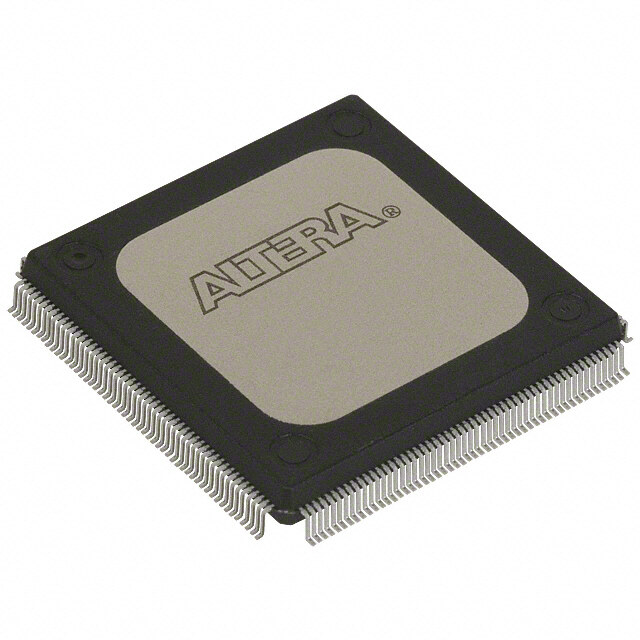
| 品牌 | Altera |
| 产品手册 | |
| 产品图片 |
|
| rohs | 符合RoHS无铅 / 符合限制有害物质指令(RoHS)规范要求 |
| 产品系列 | 嵌入式处理器和控制器,FPGA - 现场可编程门阵列,Altera Corporation EP3C40F484I7NCyclone® III |
| mouser_ship_limit | 根据美国政府的出口法规规定,Mouser无法将此产品销售到您所在的国家。 |
| 数据手册 | 点击此处下载产品Datasheet点击此处下载产品Datasheet点击此处下载产品Datasheet点击此处下载产品Datasheet点击此处下载产品Datasheet点击此处下载产品Datasheet点击此处下载产品Datasheet点击此处下载产品Datasheet |
| 产品型号 | EP3C40F484I7N |
| PCN设计/规格 | |
| 产品 | Cyclone III |
| 产品培训模块 | http://www.digikey.cn/PTM/IndividualPTM.page?site=cn&lang=zhs&ptm=15612http://www.digikey.cn/PTM/IndividualPTM.page?site=cn&lang=zhs&ptm=25437http://www.digikey.cn/PTM/IndividualPTM.page?site=cn&lang=zhs&ptm=25450 |
| 产品种类 | FPGA - 现场可编程门阵列 |
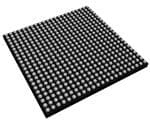
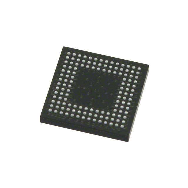
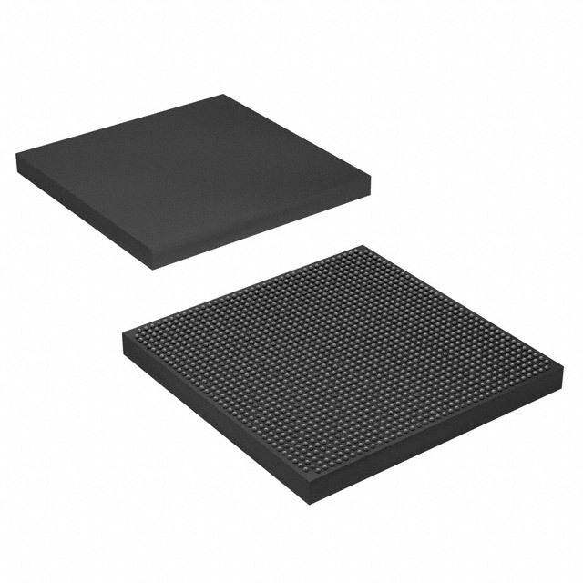
| 供应商器件封装 | 484-FBGA(23x23) |
| 其它名称 | 544-2548 |
| 商标 | Altera Corporation |
| 安装类型 | 表面贴装 |
| 安装风格 | SMD/SMT |
| 封装 | Tray |
| 封装/外壳 | 484-BGA |
| 封装/箱体 | FBGA-484 |
| 工作温度 | -40°C ~ 100°C |
| 工作电源电压 | 1.15 V to 1.25 V |
| 工厂包装数量 | 60 |
| 总RAM位数 | 1161216 |
| 总内存 | 1161216 bit |
| 最大工作温度 | + 85 C |
| 最大工作频率 | 315 MHz |
| 最小工作温度 | - 40 C |
| 栅极数 | - |
| 标准包装 | 60 |
| 电压-电源 | 1.15 V ~ 1.25 V |
| 系列 | Cyclone III |
| 输入/输出端数量 | 331 |
| 逻辑元件/单元数 | 39600 |
| 逻辑元件数量 | 39600 |
| 逻辑数组块数量——LAB | 2475 |
| 配用 | /product-detail/zh/DK-DEV-3CLS200N/544-2601-ND/2139648/product-detail/zh/DK-N2EVAL-3C25N/544-2411-ND/1658128 |


- 商务部:美国ITC正式对集成电路等产品启动337调查
- 曝三星4nm工艺存在良率问题 高通将骁龙8 Gen1或转产台积电
- 太阳诱电将投资9.5亿元在常州建新厂生产MLCC 预计2023年完工
- 英特尔发布欧洲新工厂建设计划 深化IDM 2.0 战略
- 台积电先进制程称霸业界 有大客户加持明年业绩稳了
- 达到5530亿美元!SIA预计今年全球半导体销售额将创下新高
- 英特尔拟将自动驾驶子公司Mobileye上市 估值或超500亿美元
- 三星加码芯片和SET,合并消费电子和移动部门,撤换高东真等 CEO
- 三星电子宣布重大人事变动 还合并消费电子和移动部门
- 海关总署:前11个月进口集成电路产品价值2.52万亿元 增长14.8%


PDF Datasheet 数据手册内容提取
1. Cyclone III Device Family Overview July 2012 CIII51001-2.4 CIII51001-2.4 Cyclone® III device family offers a unique combination of high functionality, low power and low cost. Based on Taiwan Semiconductor Manufacturing Company (TSMC) low-power (LP) process technology, silicon optimizations and software features to minimize power consumption, Cyclone III device family provides the ideal solution for your high-volume, low-power, and cost-sensitive applications. To address the unique design needs, Cyclone III device family offers the following two variants: ■ Cyclone III—lowest power, high functionality with the lowest cost ■ Cyclone III LS—lowest power FPGAs with security With densities ranging from about 5,000 to 200,000 logic elements (LEs) and 0.5Megabits (Mb) to 8Mb of memory for less than ¼ watt of static power consumption, Cyclone III device family makes it easier for you to meet your power budget. Cyclone III LS devices are the first to implement a suite of security features at the silicon, software, and intellectual property (IP) level on a low-power and high-functionality FPGA platform. This suite of security features protects the IP from tampering, reverse engineering and cloning. In addition, Cyclone III LS devices support design separation which enables you to introduce redundancy in a single chip to reduce size, weight, and power of your application. This chapter contains the following sections: ■ “CycloneIIIDevice Family Features” on page1–1 ■ “CycloneIIIDevice Family Architecture” on page1–6 ■ “Reference and Ordering Information” on page1–12 Cyclone III Device Family Features Cyclone III device family offers the following features: Lowest Power FPGAs ■ Lowest power consumption with TSMC low-power process technology and Altera® power-aware design flow ■ Low-power operation offers the following benefits: ■ Extended battery life for portable and handheld applications ■ Reduced or eliminated cooling system costs ■ Operation in thermally-challenged environments ■ Hot-socketing operation support © 2012 Altera Corporation. All rights reserved. ALTERA, ARRIA, CYCLONE, HARDCOPY, MAX, MEGACORE, NIOS, QUARTUS and STRATIX words and logos are trademarks of Altera Corporation and registered in the U.S. Patent and Trademark Office and in other countries. All other words and logos identified as trademarks or service marks are the property of their respective holders as described at www.altera.com/common/legal.html. Altera warrants performance of its ISO semiconductor products to current specifications in accordance with Altera's standard warranty, but reserves the right to make changes to any products and 9001:2008 services at any time without notice. Altera assumes no responsibility or liability arising out of the application or use of any information, product, or service Registered described herein except as expressly agreed to in writing by Altera. Altera customers are advised to obtain the latest version of device specifications before relying on any published information and before placing orders for products or services. Cyclone III Device Handbook Volume 1 July 2012 Subscribe
1–2 Chapter 1: CycloneIIIDevice Family Overview CycloneIIIDevice Family Features Design Security Feature Cyclone III LS devices offer the following design security features: ■ Configuration security using advanced encryption standard (AES) with 256-bit volatile key ■ Routing architecture optimized for design separation flow with the Quartus®II software ■ Design separation flow achieves both physical and functional isolation between design partitions ■ Ability to disable external JTAG port ■ Error Detection (ED) Cycle Indicator to core ■ Provides a pass or fail indicator at every ED cycle ■ Provides visibility over intentional or unintentional change of configuration random access memory (CRAM) bits ■ Ability to perform zeroization to clear contents of the FPGA logic, CRAM, embedded memory, and AESkey ■ Internal oscillator enables system monitor and health check capabilities Increased System Integration ■ High memory-to-logic and multiplier-to-logic ratio ■ High I/O count, low-and mid-range density devices for user I/O constrained applications ■ Adjustable I/O slew rates to improve signal integrity ■ Supports I/O standards such as LVTTL, LVCMOS, SSTL, HSTL, PCI, PCI-X, LVPECL, bus LVDS (BLVDS), LVDS, mini-LVDS, RSDS, and PPDS ■ Supports the multi-value on-chip termination (OCT) calibration feature to eliminate variations over process, voltage, and temperature (PVT) ■ Four phase-locked loops (PLLs) per device provide robust clock management and synthesis for device clock management, external system clock management, and I/O interfaces ■ Five outputs per PLL ■ Cascadable to save I/Os, ease PCB routing, and reduce jitter ■ Dynamically reconfigurable to change phase shift, frequency multiplication or division, or both, and input frequency in the system without reconfiguring the device ■ Remote system upgrade without the aid of an external controller ■ Dedicated cyclical redundancy code checker circuitry to detect single-event upset (SEU) issues ■ Nios® II embedded processor for CycloneIIIdevice family, offering low cost and custom-fit embedded processing solutions Cyclone III Device Handbook July 2012 Altera Corporation Volume 1
Chapter 1: CycloneIIIDevice Family Overview 1–3 CycloneIIIDevice Family Features ■ Wide collection of pre-built and verified IP cores from Altera and Altera Megafunction Partners Program (AMPP) partners ■ Supports high-speed external memory interfaces such as DDR, DDR2, SDRSDRAM, and QDRIISRAM ■ Auto-calibrating PHY feature eases the timing closure process and eliminates variations with PVT for DDR, DDR2, and QDRIISRAM interfaces CycloneIIIdevice family supports vertical migration that allows you to migrate your device to other devices with the same dedicated pins, configuration pins, and power pins for a given package-across device densities. This allows you to optimize device density and cost as your design evolves. Table1–1 lists Cyclone III device family features. Table1–1. Cyclone III Device Family Features Number of Global Logic Total RAM 18 x 18 Maximum Family Device M9K PLLs Clock Elements Bits Multipliers User I/Os Blocks Networks EP3C5 5,136 46 423,936 23 2 10 182 EP3C10 10,320 46 423,936 23 2 10 182 EP3C16 15,408 56 516,096 56 4 20 346 EP3C25 24,624 66 608,256 66 4 20 215 Cyclone III EP3C40 39,600 126 1,161,216 126 4 20 535 EP3C55 55,856 260 2,396,160 156 4 20 377 EP3C80 81,264 305 2,810,880 244 4 20 429 EP3C120 119,088 432 3,981,312 288 4 20 531 EP3CLS70 70,208 333 3,068,928 200 4 20 429 EP3CLS100 100,448 483 4,451,328 276 4 20 429 Cyclone III LS EP3CLS150 150,848 666 6,137,856 320 4 20 429 EP3CLS200 198,464 891 8,211,456 396 4 20 429 July 2012 Altera Corporation Cyclone III Device Handbook Volume 1
1–4 Chapter 1: CycloneIIIDevice Family Overview CycloneIIIDevice Family Features Table1–2 lists Cyclone III device family package options, I/O pins, and differential channel counts. Table1–2. Cyclone III Device Family Package Options, I/O pin and Differential Channel Counts (1), (2), (3), (4), (5) Family Package E144 (7) M164 P240 F256 U256 F324 F484 U484 F780 EP3C5 94, 22 106, 28 — 182, 68 182, 68 — — — — EP3C10 94, 22 106, 28 — 182, 68 182, 68 — — — — EP3C16 84, 19 92, 23 160, 47 168, 55 168, 55 — 346, 140 346, 140 — EP3C25 82, 18 — 148, 43 156, 54 156, 54 215, 83 — — — CycloneIII (8) EP3C40 — — 128, 26 — — 195, 61 331, 127 331, 127 535, 227(6) EP3C55 — — — — — — 327, 135 327, 135 377, 163 EP3C80 — — — — — — 295, 113 295, 113 429, 181 EP3C120 — — — — — — 283, 106 — 531, 233 EP3CLS70 — — — — — — 294, 113 294, 113 429, 181 EP3CLS100 — — — — — — 294, 113 294, 113 429, 181 CycloneIII LS EP3CLS150 — — — — — — 226, 87 — 429, 181 EP3CLS200 — — — — — — 226, 87 — 429, 181 Notes to Table1–2: (1) For each device package, the first number indicates the number of the I/O pin; the second number indicates the differential channel count. (2) For more information about device packaging specifications, refer to the Cyclone III Package and Thermal Resistance webpage. (3) The I/O pin numbers are the maximum I/O counts (including clock input pins) supported by the device package combination and can be affected by the configuration scheme selected for the device. (4) All packages are available in lead-free and leaded options. (5) Vertical migration is not supported between Cyclone III and Cyclone III LS devices. (6) The EP3C40 device in the F780 package supports restricted vertical migration. Maximum user I/Os are restricted to 510 I/Os if you enable migration to the EP3C120 and are using voltage referenced I/O standards. If you are not using voltage referenced I/O standards, you can increase the maximum number of I/Os. (7) The E144 package has an exposed pad at the bottom of the package. This exposed pad is a ground pad that must be connected to the ground plane on your PCB. Use this exposed pad for electrical connectivity and not for thermal purposes. (8) All Cyclone III device UBGA packages are supported by the Quartus II software version 7.1 SP1 and later, with the exception of the UBGA packages of EP3C16, which are supported by the Quartus II software version 7.2. Cyclone III Device Handbook July 2012 Altera Corporation Volume 1
Chapter 1: CycloneIIIDevice Family Overview 1–5 CycloneIIIDevice Family Features Table1–3 lists Cyclone III device family package sizes. Table1–3. Cyclone III Device Family Package Sizes Family Package Pitch (mm) Nominal Area (mm2) Length x Width (mm mm) Height (mm) E144 0.5 484 22 22 1.60 M164 0.5 64 8 8 1.40 P240 0.5 1197 34.6 34.6 4.10 F256 1.0 289 17 17 1.55 Cyclone III U256 0.8 196 14 14 2.20 F324 1.0 361 19 19 2.20 F484 1.0 529 23 23 2.60 U484 0.8 361 19 19 2.20 F780 1.0 841 29 29 2.60 F484 1.0 529 23 23 2.60 Cyclone III LS U484 0.8 361 19 19 2.20 F780 1.0 841 29 29 2.60 Table1–4 lists Cyclone III device family speed grades. Table1–4. Cyclone III Device Family Speed Grades (Part 1 of 2) Family Device E144 M164 P240 F256 U256 F324 F484 U484 F780 C7, C8, C7, C8, C6, C7, C6, C7, EP3C5 — — — — — I7, A7 I7 C8, I7, A7 C8, I7, A7 C7, C8, C7, C8, C6, C7, C6, C7, EP3C10 — — — — — I7, A7 I7 C8, I7, A7 C8, I7, A7 C7, C8, C7, C8, C6, C7, C6, C7, C6, C7, C6, C7, EP3C16 C8 — — I7, A7 I7 C8, I7, A7 C8, I7, A7 C8, I7, A7 C8, I7, A7 C7, C8, C6, C7, C6, C7, C6, C7, EP3C25 — C8 — — — I7, A7 C8, I7, A7 C8, I7, A7 C8, I7, A7 Cyclone III C6, C7, C6, C7, C6, C7, C6, C7, EP3C40 — — C8 — — C8, I7, A7 C8, I7, A7 C8, I7, A7 C8, I7 C6, C7, C6, C7, C6, C7, EP3C55 — — — — — — C8, I7 C8, I7 C8, I7 C6, C7, C6, C7, C6, C7, EP3C80 — — — — — — C8, I7 C8, I7 C8, I7 C7, C8, EP3C120 — — — — — — C7, C8, I7 — I7 July 2012 Altera Corporation Cyclone III Device Handbook Volume 1
1–6 Chapter 1: CycloneIIIDevice Family Overview CycloneIIIDevice Family Architecture Table1–4. Cyclone III Device Family Speed Grades (Part 2 of 2) Family Device E144 M164 P240 F256 U256 F324 F484 U484 F780 C7, C8, EP3CLS70 — — — — — — C7, C8, I7 C7, C8, I7 I7 C7, C8, EP3CLS100 — — — — — — C7, C8, I7 C7, C8, I7 CycloneIII I7 LS C7, C8, EP3CLS150 — — — — — — C7, C8, I7 — I7 C7, C8, EP3CLS200 — — — — — — C7, C8, I7 — I7 Table1–5 lists Cyclone III device family configuration schemes. Table1–5. Cyclone III Device Family Configuration Schemes Configuration Scheme Cyclone III Cyclone III LS Active serial (AS) v v Active parallel (AP) v — Passive serial (PS) v v Fast passive parallel (FPP) v v Joint Test Action Group (JTAG) v v Cyclone III Device Family Architecture CycloneIIIdevice family includes a customer-defined feature set that is optimized for portable applications and offers a wide range of density, memory, embedded multiplier, and I/O options. CycloneIIIdevice family supports numerous external memory interfaces and I/O protocols that are common in high-volume applications. The QuartusII software features and parameterizable IP cores make it easier for you to use the CycloneIIIdevice family interfaces and protocols. The following sections provide an overview of the CycloneIIIdevice family features. Logic Elements and Logic Array Blocks The logic array block (LAB) consists of 16 logic elements and a LAB-wide control block. An LE is the smallest unit of logic in the CycloneIIIdevice family architecture. Each LE has four inputs, a four-input look-up table (LUT), a register, and output logic. The four-input LUT is a function generator that can implement any function with four variables. f For more information about LEs and LABs, refer to the Logic Elements and Logic Array Blocks in the Cyclone III Device Family chapter. Cyclone III Device Handbook July 2012 Altera Corporation Volume 1
Chapter 1: CycloneIIIDevice Family Overview 1–7 CycloneIIIDevice Family Architecture Memory Blocks Each M9K memory block of the CycloneIIIdevice family provides nine Kbits of on-chip memory capable of operating at up to 315 MHz for Cyclone III devices and up to 274MHz for Cyclone III LS devices. The embedded memory structure consists of M9K memory blocks columns that you can configure as RAM, first-in first-out (FIFO) buffers, or ROM. The CycloneIIIdevice family memory blocks are optimized for applications such as high throughout packet processing, embedded processor program, and embedded data storage. The QuartusII software allows you to take advantage of the M9K memory blocks by instantiating memory using a dedicated megafunction wizard or by inferring memory directly from the VHDL or Verilog source code. M9K memory blocks support single-port, simple dual-port, and true dual-port operation modes. Single-port mode and simple dual-port mode are supported for all port widths with a configuration of ×1, ×2, ×4, ×8, ×9, ×16, ×18, ×32, and ×36. True dual-port is supported in port widths with a configuration of ×1, ×2, ×4, ×8, ×9, ×16, and ×18. f For more information about memory blocks, refer to the Memory Blocks in the Cyclone III Device Family chapter. Embedded Multipliers and Digital Signal Processing Support Cyclone III devices support up to 288 embedded multiplier blocks and CycloneIII LS devices support up to 396 embedded multiplier blocks. Each block supports one individual 18×18-bit multiplier or two individual 9×9-bit multipliers. The QuartusII software includes megafunctions that are used to control the operation mode of the embedded multiplier blocks based on user parameter settings. Multipliers can also be inferred directly from the VHDL or Verilog source code. In addition to embedded multipliers, CycloneIIIdevice family includes a combination of on-chip resources and external interfaces, making them ideal for increasing performance, reducing system cost, and lowering the power consumption of digital signal processing (DSP) systems. You can use CycloneIII device family alone or as DSP device co-processors to improve price-to-performance ratios of DSP systems. The CycloneIIIdevice family DSP system design support includes the following features: ■ DSP IP cores: ■ Common DSP processing functions such as finite impulse response (FIR), fast Fourier transform (FFT), and numerically controlled oscillator (NCO) functions ■ Suites of common video and image processing functions ■ Complete reference designs for end-market applications ■ DSP Builder interface tool between the QuartusII software and the MathWorks Simulink and MATLAB design environments ■ DSP development kits f For more information about embedded multipliers and digital signal processing support, refer to the Embedded Multipliers in Cyclone III Devices chapter. July 2012 Altera Corporation Cyclone III Device Handbook Volume 1
1–8 Chapter 1: CycloneIIIDevice Family Overview CycloneIIIDevice Family Architecture Clock Networks and PLLs CycloneIII device family includes 20 global clock networks. You can drive global clock signals from dedicated clock pins, dual-purpose clock pins, user logic, and PLLs. CycloneIII device family includes up to four PLLs with five outputs per PLL to provide robust clock management and synthesis. You can use PLLs for device clock management, external system clock management, and I/O interfaces. You can dynamically reconfigure the CycloneIII device family PLLs to enable auto-calibration of external memory interfaces while the device is in operation. This feature enables the support of multiple input source frequencies and corresponding multiplication, division, and phase shift requirements. PLLs in CycloneIII device family may be cascaded to generate up to ten internal clocks and two external clocks on output pins from a single external clock source. f For more PLL specifications and information, refer to the Cyclone III Device Data Sheet, Cyclone III LS Device Data Sheet, and Clock Networks and PLLs in the Cyclone III Device Family chapters. I/O Features CycloneIII device family has eight I/O banks. All I/O banks support single-ended and differential I/O standards listed in Table1–6. Table1–6. CycloneIII Device Family I/O Standards Support Type I/O Standard Single-Ended I/O LVTTL, LVCMOS, SSTL, HSTL, PCI, and PCI-X Differential I/O SSTL, HSTL, LVPECL, BLVDS, LVDS, mini-LVDS, RSDS, and PPDS The CycloneIIIdevice family I/O also supports programmable bus hold, programmable pull-up resistors, programmable delay, programmable drive strength, programmable slew-rate control to optimize signal integrity, and hot socketing. CycloneIII device family supports calibrated on-chip series termination (R OCT) or S driver impedance matching (Rs) for single-ended I/O standards, with one OCT calibration block per side. f For more information, refer to the I/O Features in the Cyclone III Device Family chapter. High-Speed Differential Interfaces CycloneIII device family supports high-speed differential interfaces such as BLVDS, LVDS, mini-LVDS, RSDS, and PPDS. These high-speed I/O standards in CycloneIII device family provide high data throughput using a relatively small number of I/O pins and are ideal for low-cost applications. Dedicated differential output drivers on the left and right I/O banks can send data rates at up to 875Mbps for Cyclone III devices and up to 740 Mbps for Cyclone III LS devices, without the need for external resistors. This saves board space or simplifies PCB routing. Top and bottom I/O banks support differential transmission (with the addition of an external resistor network) data rates at up to 640 Mbps for both Cyclone III and Cyclone III LS devices. Cyclone III Device Handbook July 2012 Altera Corporation Volume 1
Chapter 1: CycloneIIIDevice Family Overview 1–9 CycloneIIIDevice Family Architecture f For more information, refer to the High-Speed Differential Interfaces in the CycloneIII Device Family chapter. Auto-Calibrating External Memory Interfaces CycloneIII device family supports common memory types such as DDR, DDR2, SDRSDRAM, and QDRII SRAM. DDR2SDRAM memory interfaces support data rates up to 400 Mbps for Cyclone III devices and 333 Mbps for Cyclone III LS devices. Memory interfaces are supported on all sides of CycloneIIIdevice family. CycloneIII device family has the OCT, DDR output registers, and 8-to-36-bit programmable DQ group widths features to enable rapid and robust implementation of different memory standards. An auto-calibrating megafunction is available in the QuartusII software for DDR and QDR memory interface PHYs. This megafunction is optimized to take advantage of the CycloneIII device family I/O structure, simplify timing closure requirements, and take advantage of the CycloneIII device family PLL dynamic reconfiguration feature to calibrate PVT changes. f For more information, refer to the External Memory Interfaces in the CycloneIII Device Family chapter. Support for Industry-Standard Embedded Processors To quickly and easily create system-level designs using CycloneIII device family, you can select among the ×32-bit soft processor cores: Freescale®V1 Coldfire, ARM® CortexM1, or Altera Nios®II, along with a library of 50 other IP blocks when using the system-on-a-programmable-chip (SOPC) Builder tool. SOPC Builder is an Altera QuartusII design tool that facilitates system-integration of IP blocks in an FPGA design. The SOPC Builder automatically generates interconnect logic and creates a testbench to verify functionality, saving valuable design time. CycloneIII device family expands the peripheral set, memory, I/O, or performance of legacy embedded processors. Single or multiple NiosII embedded processors are designed into CycloneIII device family to provide additional co-processing power, or even replace legacy embedded processors in your system. Using the CycloneIII device family and NiosII together provide low-cost, high-performance embedded processing solutions, which in turn allow you to extend the life cycle of your product and improve time-to-market over standard product solutions. 1 Separate licensing of the Freescale and ARM embedded processors are required. Hot Socketing and Power-On-Reset CycloneIII device family features hot socketing (also known as hot plug-in or hot swap) and power sequencing support without the use of external devices. You can insert or remove a board populated with one or more CycloneIII device family during a system operation without causing undesirable effects to the running system bus or the board that was inserted into the system. July 2012 Altera Corporation Cyclone III Device Handbook Volume 1
1–10 Chapter 1: CycloneIIIDevice Family Overview CycloneIIIDevice Family Architecture The hot socketing feature allows you to use FPGAs on PCBs that also contain a mixture of 3.3-V, 2.5-V, 1.8-V, 1.5-V, and 1.2-V devices. The CycloneIII device family hot socketing feature eliminates power-up sequence requirements for other devices on the board for proper FPGA operation. f For more information about hot socketing and power-on-reset, refer to the Hot-Socketing and Power-on Reset in the Cyclone III Device Family chapter. SEU Mitigation CycloneIIILS devices offer built-in error detection circuitry to detect data corruption due to soft errors in the CRAM cells. This feature allows CRAM contents to be read and verified to match a configuration-computed CRC value. The QuartusII software activates the built-in 32-bit CRC checker, which is part of the CycloneIIILS device. f For more information about SEU mitigation, refer to the SEU Mitigation in the CycloneIII Device Family chapter. JTAG Boundary Scan Testing CycloneIII device family supports the JTAG IEEE Std. 1149.1 specification. The boundary-scan test (BST) architecture offers the capability to test pin connections without using physical test probes and captures functional data while a device is operating normally. Boundary-scan cells in the CycloneIII device family can force signals onto pins or capture data from pins or from logic array signals. Forced test data is serially shifted into the boundary-scan cells. Captured data is serially shifted out and externally compared to expected results. In addition to BST, you can use the IEEE Std. 1149.1 controller for the CycloneIIILS device in-circuit reconfiguration (ICR). f For more information about JTAG boundary scan testing, refer to the IEEE 1149.1 (JTAG) Boundary-Scan Testing for the Cyclone III Device Family chapter. Quartus II Software Support The QuartusII software is the leading design software for performance and productivity. It is the only complete design solution for CPLDs, FPGAs, and ASICs in the industry. The QuartusII software includes an integrated development environment to accelerate system-level design and seamless integration with leading third-party software tools and flows. The Cyclone III LS devices provide both physical and functional separation between security critical design partitions. Cyclone III LS devices offer isolation between design partitions. This ensures that device errors do not propagate from one partition to another, whether unintentional or intentional. The QuartusII software design separation flow facilitates the creation of separation regions in CycloneIIILS devices by tightly controlling the routing in and between the LogicLock regions. For ease of use, the separation flow integrates in the existing incremental compilation flow. f For more information about the Quartus II software features, refer to the Quartus II Handbook. Cyclone III Device Handbook July 2012 Altera Corporation Volume 1
Chapter 1: CycloneIIIDevice Family Overview 1–11 CycloneIIIDevice Family Architecture Configuration CycloneIII device family uses SRAM cells to store configuration data. Configuration data is downloaded to CycloneIII device family each time the device powers up. Low-cost configuration options include the Altera EPCS family serial flash devices as well as commodity parallel flash configuration options. These options provide the flexibility for general-purpose applications and the ability to meet specific configuration and wake-up time requirements of the applications. CycloneIII device family supports the AS, PS, FPP, and JTAG configuration schemes. The AP configuration scheme is only supported in Cyclone III devices. f For more information about configuration, refer to the Configuration, Design Security, and Remote System Upgrades in the Cyclone III Device Family chapter. Remote System Upgrades CycloneIII device family offers remote system upgrade without an external controller. The remote system upgrade capability in CycloneIII device family allows system upgrades from a remote location. Soft logic (either the NiosII embedded processor or user logic) implemented in CycloneIII device family can download a new configuration image from a remote location, store it in configuration memory, and direct the dedicated remote system upgrade circuitry to start a reconfiguration cycle. The dedicated circuitry performs error detection during and after the configuration process, and can recover from an error condition by reverting to a safe configuration image. The dedicated circuitry also provides error status information. Cyclone III devices support remote system upgrade in the AS and AP configuration scheme. Cyclone III LS devices support remote system upgrade in the AS configuration scheme only. f For more information, refer to the Configuration, Design Security, and Remote System Upgrades in the CycloneIII Device Family chapter. Design Security (Cyclone III LS Devices Only) Cyclone III LS devices offer design security features which play a vital role in the large and critical designs in the competitive military and commercial environments. Equipped with the configuration bit stream encryption and anti-tamper features, Cyclone III LS devices protect your designs from copying, reverse engineering and tampering. The configuration security of Cyclone III LS devices uses AES with 256-bit security key. f For more information, refer to the Configuration, Design Security, and Remote System Upgrades in Cyclone III Device Family chapter. July 2012 Altera Corporation Cyclone III Device Handbook Volume 1
1–12 Chapter 1: CycloneIIIDevice Family Overview Reference and Ordering Information Reference and Ordering Information Figure1–1 and Figure1–2 show the ordering codes for Cyclone III and CycloneIIILS devices. Figure1–1. Cyclone III Device Packaging Ordering Information Package Type E : Plastic Enhanced Quad Flat Pack (EQFP) Q : Plastic Quad Flat Pack (PQFP) Operating Temperature F : FineLine Ball-Grid Array (FBGA) C : Commercial temperature (T = 0° C to 85° C) U : Ultra FineLine Ball-Grid Array (UBGA) J I : Industrial temperature (T = -40° C to 100° C) M : Micro FineLine Ball-Grid Array (MBGA) J A : Automotive temperature (T = -40° C to 125° C) J Family Signature EP3C 25 F 324 C 7 N Optional Suffix EP3C : Cyclone III Indicates specific device options or shipment method Member Code Package Code N : Lead-free packaging 5 : 5,136 logic elements 144 : 144 pins ES : Engineering sample 10 : 10,320 logic elements 164 : 164 pins Speed Grade 16 : 15,408 logic elements 240 : 240 pins 25 : 24,624 logic elements 256 : 256 pins 6 (fastest) 25E : 24,624 logic elements 324 : 324 pins 7 40 : 39,600 logic elements 484 : 484 pins 8 55 : 55,856 logic elements 780 : 780 pins 80 : 81,264 logic elements 120 : 119,088 logic elements Figure1–2. Cyclone III LS Device Packaging Ordering Information Package Type Operating Temperature F : FineLine Ball-Grid Array (FBGA) C : Commercial temperature (T = 0° C to 85° C) J U : Ultra FineLine Ball-Grid Array (UBGA) I : Industrial temperature (T = -40° C to 100° C) J Family Signature EP3CLS 70 F 484 C 7 N Optional Suffix EP3CLS : Cyclone III LS Indicates specific device options or shipment method Member Code Package Code N : Lead-free packaging 70 : 70,208 logic elements 484 : 484 pins ES : Engineering sample 100 : 100,448 logic elements 780 : 780 pins Speed Grade 150 : 150,848 logic elements 200 : 198,464 logic elements 7 (fastest) 8 Cyclone III Device Handbook July 2012 Altera Corporation Volume 1
Chapter 1: CycloneIIIDevice Family Overview 1–13 Document Revision History Document Revision History Table1–7 lists the revision history for this document. Table1–7. Document Revision History Date Version Changes July 2012 2.4 Updated 484 pin package code in Figure1–1. ■ Updated Table1–1 and Table1–2. ■ Updated Figure1–1 and Figure1–2. December 2011 2.3 ■ Updated hyperlinks. ■ Minor text edits. December 2009 2.2 Minor text edits. July 2009 2.1 Minor edit to the hyperlinks. ■ Added Table1–5. ■ Updated Table1–1, Table1–2, Table1–3, and Table1–4. ■ Updated “Introduction”, “CycloneIIIDevice Family Architecture”, “Embedded Multipliers and Digital Signal Processing Support ”, “Clock Networks and PLLs ”, “I/O Features ”, June 2009 2.0 “High-Speed Differential Interfaces ”, “Auto-Calibrating External Memory Interfaces ”, “QuartusII Software Support”, “Configuration ”, and “Design Security (Cyclone III LS Devices Only)”. ■ Removed “Referenced Document” section. ■ Updated “Increased System Integration” section. October 2008 1.3 ■ Updated “Memory Blocks” section. ■ Updated chapter to new template. ■ Added 164-pin Micro FineLine Ball-Grid Array (MBGA) details to Table 1–2, Table 1–3 and Table 1–4. May 2008 1.2 ■ Updated Figure 1–2 with automotive temperature information. ■ Updated “Increased System Integration” section, Table 1–6, and “High-Speed Differential Interfaces” section with BLVDS information. ■ Removed the text “Spansion” in “Increased System. ■ Integration” and “Configuration” sections. ■ Removed trademark symbol from “MultiTrack” in “MultiTrack Interconnect”. July 2007 1.1 ■ Removed registered trademark symbol from “Simulink” and “MATLAB” from “Embedded Multipliers and Digital. ■ Signal Processing Support” section. ■ Added chapter TOC and “Referenced Documents” section. March 2007 1.0 Initial release. July 2012 Altera Corporation Cyclone III Device Handbook Volume 1
1–14 Chapter 1: CycloneIIIDevice Family Overview Document Revision History Cyclone III Device Handbook July 2012 Altera Corporation Volume 1
Mouser Electronics Authorized Distributor Click to View Pricing, Inventory, Delivery & Lifecycle Information: I ntel: EP3C25Q240C8N EP3CLS150F484I7N EP3C5E144C7N EP3CLS100F484C7 EP3C16E144C7 EP3C16F484C8 EP3C5F256C8 EP3CLS70F484C7N EP3C55F484I7 EP3CLS100F484C8N EP3C10E144C7 EP3C40F484C6 EP3C16U484C8 EP3C40F324A7N EP3C80F484C8 EP3C25F324A7N EP3C55U484C6 EP3C40U484C8 EP3C80F484I7N EP3C5U256C7 EP3C40F780C7 EP3C80F780I7 EP3C40F780C8N EP3CLS70F780I7N EP3C120F484C8N EP3C80U484C6N EP3C40F484I7N EP3C16U256C7N EP3CLS200F484C7 EP3C10M164I7N EP3C25E144C8 EP3C55F484C7N EP3C55F780C8N EP3C80F484C6N EP3CLS150F484C8 EP3C16F256C6 EP3C40F324I7 EP3C40Q240C8N EP3C25F256C7 EP3C16U256I7N EP3C25F256C8N EP3CLS100U484I7N EP3C10F256I7N EP3C10F256C6 EP3C120F484C7 EP3C25F324C8N EP3C55U484I7N EP3C5E144C7 EP3C25F324I7 EP3C25F256C8 EP3C16U484C6 EP3C16F484C6N EP3C55U484I7 EP3CLS150F484C7N EP3C80F484C7N EP3C40U484C6 EP3C25U256C8 EP3CLS150F484I7 EP3C55F484C7 EP3CLS100F780C7N EP3C5F256C6N EP3C5U256C6N EP3C120F484C8 EP3C80F780C8N EP3C80U484C8 EP3C16F484C6 EP3C16F484C7N EP3CLS70F780I7 EP3CLS100F780I7 EP3CLS100U484I7 EP3C5E144I7 EP3C25E144C7N EP3CLS200F484C8 EP3C55F780C8 EP3CLS70F484I7 EP3C25Q240C8 EP3C25F256C6N EP3CLS100F780C8N EP3C120F780C7 EP3CLS150F780C8 EP3CLS150F780I7N EP3C40F484C7N EP3C40U484I7N EP3C10F256I7 EP3C40Q240C8 EP3C55F780C6N EP3C80F484C6 EP3CLS70U484I7N EP3C16F256A7N EP3CLS200F780C7 EP3C16F256I7 EP3C55U484C7N EP3C10E144C8N EP3CLS70F780C7N EP3C10E144C8 EP3C80F780C6N EP3C5M164C8N EP3CLS200F780C8 EP3C40U484I7 EP3C10U256C8